EP0915583B1 - Wellenlängenmultiplex-Übertragungsvorrichtung - Google Patents
Wellenlängenmultiplex-Übertragungsvorrichtung Download PDFInfo
- Publication number
- EP0915583B1 EP0915583B1 EP98104398A EP98104398A EP0915583B1 EP 0915583 B1 EP0915583 B1 EP 0915583B1 EP 98104398 A EP98104398 A EP 98104398A EP 98104398 A EP98104398 A EP 98104398A EP 0915583 B1 EP0915583 B1 EP 0915583B1
- Authority
- EP
- European Patent Office
- Prior art keywords
- optical
- excitation light
- signals
- section
- optimal
- Prior art date
- Legal status (The legal status is an assumption and is not a legal conclusion. Google has not performed a legal analysis and makes no representation as to the accuracy of the status listed.)
- Expired - Lifetime
Links
Images


Classifications
-
- H—ELECTRICITY
- H04—ELECTRIC COMMUNICATION TECHNIQUE
- H04J—MULTIPLEX COMMUNICATION
- H04J14/00—Optical multiplex systems
- H04J14/02—Wavelength-division multiplex systems
- H04J14/0221—Power control, e.g. to keep the total optical power constant
Definitions
- the present invention relates to a wavelength division multiplex optical transmission apparatus in which a plurality of optical signals having different wavelengths are processed by wavelength division multiplexing, and are transmitted to an optical transmission line.
- WDM wavelength division multiplexing
- the most dominant type is a WDM unit in which, for example, a WDM coupler is used to process by the wavelength division multiplexing the plurality of optical signals having the different wavelengths ⁇ 1 to ⁇ n, and a concurrent optical amplification is subsequently made to the optical signals with the wavelengths ⁇ 1 to ⁇ n to desired optical signal levels so as to output the optical signals to the optical transmission line, thereby transmitting all the optical signals with the wavelengths ⁇ 1 to ⁇ n to an opposite side.
- a WDM coupler is used to process by the wavelength division multiplexing the plurality of optical signals having the different wavelengths ⁇ 1 to ⁇ n, and a concurrent optical amplification is subsequently made to the optical signals with the wavelengths ⁇ 1 to ⁇ n to desired optical signal levels so as to output the optical signals to the optical transmission line, thereby transmitting all the optical signals with the wavelengths ⁇ 1 to ⁇ n to an opposite side.
- the concurrent optical amplification is made though distances for which the optical signals with the wavelengths ⁇ 1 to ⁇ n can be transmitted may be varied for the wavelengths ⁇ 1 to ⁇ n depending upon states (such as loss) of the optical transmission line.
- states such as loss
- a higher optical output level must be provided for an optical signal with the wavelength which can ensure a sufficiently long transmission distance even at a low send optical output level. Therefore, an increase in power consumption of the transmission apparatus results in a significantly high transmission cost.
- the optical signal is amplified by using an optical amplification fiber such as erbium-doped fiber, and launching, together with a transmit optical signal, an excitation optical signal having desired power into the optical amplification fiber.
- an optical amplification fiber such as erbium-doped fiber
- launching, together with a transmit optical signal, an excitation optical signal having desired power into the optical amplification fiber there is a complicated correlation between an amplification factor (signal net gain) and incident excitation light power at a time of optical amplification.
- an amplification factor signal net gain
- the variation causes a variation in optical amplification factor, thereby varying the optical output level after the optical amplification. Consequently, the optical signals with the wavelengths ⁇ 1 to ⁇ n cannot have optical output levels suitable for the transmission distances of the wavelengths ⁇ 1 to ⁇ n. Accordingly, it is impossible to employ a simple method of adjusting the optical output level after the amplification by using an optical attenuator or the like.
- GB 2 294 170 discloses an optical amplifier, for amplifying a wavelength-division-multiplexed optical input signal composed of optical signals having different wavelengths, with means for controlling its output level according to the number of the optical signals, to optimise the output level of each of the optical signals. If the number of optical signals is two, the difference between the respective gains of the amplifier for the two optical signals is reduced by simultaneous excitation of a doped optical fibre, in the amplifier, by two different excitation beams.
- US 5 675 432 relates to an optical amplification apparatus for adjusting optical power of wavelength-multiplexed signal light at respective wavelengths and for adjusting the optical output power at the respective wavelengths and a deviation of the optical output power between the wavelengths.
- An optical power adjusting unit for receiving inputted light having signal light at a plurality of different wavelengths multiplexed thereon, amplifying or attenuating light at least one wavelength included in the received light independently of light at different wavelengths from the wavelength of the light, is provided before or after an optical amplifier unit for amplifying the light having the signal light at the plurality of different wavelengths multiplexed thereon. Further a control unit is provided for controlling the gain of amplification or attenuation performed by the optical power adjusting unit and the gain of amplification performed by the optical amplifier unit, respectively.
- JP 09098136 shows a further relevant prior art multiplexing apparatus.
- a wavelength division multiplex optical transmission apparatus in which a plurality of optical signals having different wavelengths are processed by wavelength division multiplexing, and are transmitted through an optical transmission line.
- the apparatus includes an optical sending system having a plurality of optical sending sections to generate and transmit the optical signals having the different wavelengths, a plurality of optical amplifying sections to amplify the optical signals with the wavelengths from the optical sending sections, and a wavelength division multiplexing section to process by the wavelength division multiplexing and output to the optical transmission line the optical signals amplified in the optical amplifying sections, and an optical receiving system having a wavelength division demultiplexing section to demultiplex the wavelength division multiplexed optical signals transmitted through the optical transmission line into the optical signals with the wavelengths, and a plurality of optical receiving sections to receive the optical signals demultiplexed in the wavelength division demultiplexing section.
- an optical output level control section is mounted to control, for the wavelengths, optical output levels of the optical signals output to the optical transmission line through the wavelength division multiplexing section) by individually
- a wavelength division multiplex optical transmission apparatus in which a plurality of optical signals having different wavelengths are processed by wavelength division multiplexing, and are transmitted through an optical transmissionline.
- the apparatus includes an optical sending system having a plurality of optical sending sections to generate and transmit the optical signals having the different wavelengths, and a wavelength division multiplexing section to process by the wavelength division multiplexing and output to the optical transmission line the optical signals with the wavelengths from the optical sending sections.
- an optical output level adjusting section is mounted to control, for the wavelengths, optical output levels of the optical signals with the wavelengths, sent to the optical transmission line before the wavelength division multiplexing by the wavelength division multiplexing section in the optical sending system.
- the optical output level adjusting section may include a plurality of optical amplifying sections interposed between the optical sending sections and the wavelength division multiplexing section to amplify the optical signals with the wavelengths from the optical sending sections, and an optical output level control section to control, for the wavelengths, optical output levels of the optical signals output to the optical transmission line through the wavelength division multiplexing section by individually varying amplification factors in the optical amplifying sections.
- the optical output level control section controls, for the wavelengths, the optical output levels of the optical signals to the optical transmission line (that is, adjusts, for the wavelengths, the optical output levels of the optical signals with the wavelengths before the wavelength division multiplexing) by individually varying the amplification factors in the plurality of optical amplifying sections to respectively amplify the optical signals with the plurality of wavelengths, to be transmitted after the wavelength division multiplexing in the optical sending system. Therefore, it is possible to transmit the respective optical signals at the optical output levels most suitable for the optical signals with consideration given to characteristics inherent in the optical signals with the wavelengths. Thereby, the respective optical signals can always be sent at the minimum optical output levels. As a result, it is possible to significantly reduce power consumption at a time of optical transmission, and realize the optical transmission at a lower cost as compared with the case where the optical signals with the wavelengths are concurrently amplified after the wavelength division multiplexing.
- the optical output level control section may include a plurality of excitation light sources to generate excitation light signals for varying the amplification factors in the optical amplifying sections, a plurality of excitation light output level adjusting sections which can adjust optical output levels of the excitation light signals generated in the excitation light sources, and an excitation light output level operation control section to find optimal optical output levels of the optical signals according to transmission distances of the optical signals with the wavelengths, generated in the optical sending sections, and control the excitation light output level adjusting sections according to the optimal optical output levels to adjust the optical output levels of the excitation light signals.
- the optical signals with the wavelengths can always be sent at the optimal optical output levels according to the transmission distances of the respective wavelengths.
- the optical signals can be sent at the minimum optical output levels required for a predetermined optical transmission distance.
- the excitation light output level operation control section may include a parameter input section to take as inputs predetermined parameter information about the optical transmission line, containing at least information about the transmission distances of the optical signals with the wavelengths, to be output to the optical transmission line, an optimal optical output level operation section to find by predetermined arithmetic operations optimal optical output levels of the optical signals according to the transmission distances of the optical signals with the wavelengths depending upon the parameter information input through the parameter input section, and an excitation light adjusting signal generating section to generate excitation light adjusting signals for adjusting the optical output levels of the excitation light signals depending upon the optimal optical output levels obtained by the optimal optical output level operation section.
- the optical output levels most suitable for the optical signals with the respective wavelengths are automatically calculated to generate the excitation light adjusting signals for adjusting the optical output levels of the excitation light signals (the type finding the optimal optical output level depending upon the parameter information will hereinafter be referred to as "parameter information type"). Consequently, it is possible to significantly easily and accurately adjust the optical output levels of the optical signals with the wavelengths.
- the optical output level control section may include a plurality of excitation light sources to generate excitation light signals for varying the amplification factors in the optical amplifying sections, a plurality of excitation light output level adjusting sections which can adjust optical output levels of the excitation light signals generated in the excitation light sources, an excitation light output level operation control section to find by arithmetic operations optimal optical output levels of the optical signals according to transmission distances of the optical signals with the wavelengths, generated in the optical sending sections, and control the excitation light output level adjusting sections according to the optimal optical output levels to adjust the optical output levels of the excitation light signals, and a plurality of input signal light receiving sections to respectively receive the optical signals with the wavelengths, input through the optical transmission line and demultiplexed in the wavelength division demultiplexing section.
- the excitation light output level operation control section may include a transmission loss operation section to find by predetermined arithmetic operations transmission loss information of the optical signals actually transmitted through the optical transmission line for a predetermined transmission distance depending upon the optical signals with the wavelengths, received in the input signal light receiving sections, an optimal optical output level operation section to find by predetermined arithmetic operations optimal optical output levels of the optical signals with the wavelengths depending upon the transmission loss information obtained in the transmission loss operation section, and an excitation light adjusting signal generating section to generate excitation light adjusting signals for adjusting the optical output levels of the excitation light signals depending upon the optimal excitation light levels obtained in the optimal optical output level operation section.
- the optimal optical output levels of the optical signals with the respective wavelengths are respectively found by the predetermined arithmetic operations depending upon the transmission loss information of the optical signals with the respective wavelengths, actually transmitted through the optical transmission line for the predetermined transmission distance. Further, it is possible to generate the excitation light adjusting signals for adjusting the optical output levels of the excitation light signals depending upon the obtained optimal optical output levels (the type finding the optimal optical output level depending upon the transmission loss information will hereinafter be referred to as "transmission loss type"). Consequently, it is possible to adjust the optical output levels of the optical signals with the respective wavelengths with consideration given to an actual state (loss) of the optical transmission line. Besides, it is possible to more accurately adjust to the optimal values the optical output levels of the optical signals with the respective wavelengths.
- the optical output level control section may include a plurality of excitation light sources to generate excitation light signals for varying the amplification factors in the optical amplifying sections, a plurality of excitation light output level adjusting sections which can adjust optical output levels of the excitation light signals generated in the excitation light sources, an excitation light output level operation control section to find by arithmetic operations optimal optical output levels of the optical signals according to transmission distances of the optical signals with the wavelengths, generated in the optical sending sections, and control the excitation light output level adjusting sections according to the optimal optical output levels to adjust the optical output levels of the excitation light signals, a plurality of input signal light receiving sections to receive the optical signals with the wavelengths, input through the optical transmission line and demultiplexed in the wavelength division demultiplexing section, and a plurality of output signal light receiving sections to respectively receive parts of the optical signals with the wavelengths, to be output to the optical transmission line through the wavelength division multiplexing section after amplification in the optical amplifying sections.
- the excitation light output level operation control section may include a transmission loss operation section to find by predetermined arithmetic operations transmission loss information of the optical signals actually transmitted through the optical transmission line for a predetermined transmission distance depending upon the optical signals with the wavelengths, received in the input signal light receiving sections, an optimal optical output level operation section to find by predetermined arithmetic operations optimal optical output levels of the optical signals with the wavelengths depending upon the transmission loss information obtained in the transmission loss operation section, an excitation light adjusting signal generating section to generate excitation light adjusting signals for the excitation light output level adjusting sections depending upon the optimal excitation light levels obtained in the optimal optical output level operation section, a level comparing section to compare the optimal optical output levels with optical signal levels of the optical signals received in the output signal light receiving sections, and a level error correcting section to correct, if errors are caused between the respective levels as a result of comparison in the level comparing section, generation processing for the excitation light adjusting signals so as to minimize the errors.
- a transmission loss operation section to find by predetermined arith
- correction function the optical output levels of the optical signals with the wavelengths are varied due to the characteristics of the optical amplifiers, disturbance, and so forth, it is possible to continuously stabilize the optical output levels of the respective wavelengths at the optimal levels while following the variations, resulting in significantly enhanced performance of the transmission apparatus.
- the optical output level control section may include a plurality of excitation light sources to generate excitation light signals for varying the amplification factors in the optical amplifying sections, a plurality of excitation light output level adjusting sections which can adjust optical output levels of the excitation light signals generated in the excitation light sources, an excitation light output level operation control section to find by arithmetic operations optimal optical output levels of the optical signals according to transmission distances of the optical signals with the wavelengths, generated in the optical sending sections, and control the excitation light output level adjusting sections according to the optimal optical output levels to adjust the optical output levels of the excitation light signals, and excitation light signal receiving sections which can receive the excitation light signals returning from the optical transmission line through the wavelength division demultiplexing section when the optical transmission line is in a disconnection state.
- the optical sending system may be provided to output both the optical signals from the optical amplifying sections and the excitation light signals from the excitation light sources to the optical transmission line through the wavelength division multiplexing section.
- the excitation light output level operation control section may include a parameter input section to take as inputs predetermined parameter information about the optical transmission line, containing at least information about the transmission distances of the optical signals with the wavelengths, to be output to the optical transmission line, an optimal optical output level operation section to find by predetermined arithmetic operations optimal optical output levels of the optical signals according to the transmission distances of the optical signals with the wavelengths, generated in the optical sending sections depending upon the parameter information input through the parameter input section, an excitation light adjusting signal generating section to generate excitation light adjusting signals for adjusting the optical output levels of the excitation light signals depending upon the optimal optical output levels obtained by the optimal optical output level operation section, an excitation light adjusting signal generating section to generate excitation light adjusting signals for adjusting the optical output levels of the excitation light signals depending upon the optimal optical output levels of the
- the "parameter information type" of excitation light output level operation control section decides that the optical transmission line is in the disconnection state, and can set the optical output levels of the excitation light signals to zeros and can give the alarm (hereinafter referred to as optical transmission line disconnection state detecting function). Consequently, it is possible to reduce unnecessary output of the excitation light signals so as to reduce power consumption when the optical transmission line is in the disconnection state. Concurrently, it is possible to more surely post the disconnection state of the optical transmission line to the outside. Further, it is possible to realize the optical transmission line disconnection state detecting function at a lower cost since the disconnection state of the optical transmission line is detected by using detection (receive) of return optical signals of the excitation light signals.
- the optical output level control section may include a plurality of excitation light sources to generate excitation light signals for varying the amplification factors in the optical amplifying sections, a plurality of excitation light output level adjusting sections which can adjust optical output levels of the excitation light signals generated in the excitation light sources, an excitation light output level operation control section to find by arithmetic operations optimal optical output levels of the optical signals according to transmission distances of the optical signals with the wavelengths, generated in the optical sending sections, and control the excitation light output level adjusting sections according to the optimal optical output levels to adjust the optical output levels of the excitation light signals, a plurality of input signal light receiving sections to respectively receive the optical signals with the wavelengths, input through the optical transmission line and demultiplexed in the wavelength division demultiplexing section, and excitation light signal receiving sections which can receive the excitation light signals returning from the optical transmission line through the wavelength division demultiplexing section when the optical transmission line is in a disconnection state.
- the optical sending system may be provided to output both the optical signals from the optical amplifying sections and the excitation light signals from the excitation light sources to the optical transmission line through the wavelength division multiplexing section.
- the excitation light output level operation control section may include a transmission loss operation section to find by predetermined arithmetic operations transmission loss information of the optical signals actually transmitted through the optical transmission line for a predetermined transmission distance depending upon the optical signals with the wavelengths, received in the input signal light receiving sections, an optimal optical output level operation section to find by predetermined arithmetic operations optimal optical output levels of the optical signals with the wavelengths depending upon the transmission loss information obtained by the transmission loss operation section, an excitation light adjusting signal generating section to generate excitation light adjusting signals for the excitation light output level adjusting sections depending upon the optimal excitation light levels obtained in the optimal optical output level operation section, an excitation light reception decision section to decide whether or not the excitation light signals have been received in the excitation light signal receiving sections, a disconnection state control section to decide that the optical transmission line is in
- the "transmission loss information type" of excitation light output level operation control section may have the "optical transmission line disconnection state detecting function" as in the “parameter information type” of that. It is thereby possible to reduce power consumption when the optical transmission line is in the disconnection state, and more surely post the disconnection state of the optical transmission line to the outside. Further, in this case, it is also possible to realize the optical transmission line disconnection state detecting function at a lower cost since the disconnection state of the optical transmission line is detected by using detection (receive) of the return optical signals of the excitation light signals.
- the optical output level control section may include a plurality of excitation light sources to generate excitation light signals for varying the amplification factors in the optical amplifying sections, a plurality of excitation light output level adjusting sections which can adjust optical output levels of the excitation light signals generated in the excitation light sources, an excitation light output level operation control section to find by arithmetic operations optimal optical output levels of the optical signals according to transmission distances of the optical signals with the wavelengths, generated in the optical sending sections, and control the excitation light output level adjusting sections according to the optimal optical output levels to adjust the optical output levels of the excitation light signals, a plurality of input signal light receiving sections to respectively receive the optical signals with the wavelengths, input through the optical transmission line and demultiplexed in the wavelength division demultiplexing section, a plurality of output signal light receiving sections to respectively receive parts of the optical signals with the wavelengths, to be output to the optical transmission line through the wavelength division multiplexing section after amplification in the optical amplifying sections, excitation light signal receiving sections which can receive
- the optical sending system may be provided to output both the optical signals from the optical amplifying sections and the excitation light signals from the excitation light sources to the optical transmission line through the wavelength division multiplexing section.
- the excitation light output level operation control section may include a transmission loss operation section to find by predetermined arithmetic operations transmission loss information of the optical signals actually transmitted through the optical transmission line for a predetermined transmission distance depending upon the optical signals with the wavelengths, received in the input signal light receiving sections, an optimal optical output level operation section to find by predetermined arithmetic operations optimal optical output levels of the optical signals with the wavelengths depending upon the transmission loss information obtained in the transmission loss operation section, an excitation light adjusting signal generating section to generate excitation light adjusting signals for the excitation light output level adjusting sections depending upon the optimal excitation light output levels obtained in the optimal optical output level operation section, a level comparing section to compare the optimal optical output levels with optical signal levels of the optical signals received in the output signal light receiving sections, a level error correcting section to correct, if errors are
- the "transmission loss information type" of excitation light output level operation control section includes the "correcting function,” and the “optical transmission line disconnection state detecting function.” Consequently, it is possible to continuously stabilize the optical output levels of the respective wavelengths at the optimal levels while following the variations in optical output levels, while reducing power consumption when the optical transmission line is in the disconnection state, and posting the disconnection state of the optical transmission line to the outside.
- the excitation light output level adjusting sections may each include a polarization section which can vary a polarization factor of the excitation optical signal from the excitation light source, and can adjust the polarization factor of the excitation optical signal by varying polarization factor of the polarization section.
- the excitation light adjusting signal generating section of the excitation light output level operation control section is provided to generate polarization factor adjusting signals for adjusting the polarization factors of the polarization sections as the excitation light adjusting signals for the excitation light output level adjusting sections.
- the excitation light output level adjusting section may generate, as the excitation light adjusting signals for the excitation light output level adjusting sections, the polarization factor adjusting signals for adjusting the polarization factors of the polariscopes. Consequently, it is possible to adjust the optical output levels of the excitation light signals at a very high speed.
- the excitation light output level adjusting sections may each include a lens which can vary a refractive index of the excitation light signal according to an incident position of the excitation light signal from the excitation light source, and can vary the incident position of the excitation light signal on the lens to vary the refractive index of the excitation light signal so as to vary the optical output level of the excitation light signal.
- the excitation light adjusting signal generating section of the excitation light output level operation control section may be provided to generate lens incident position adjusting signals for adjusting the incident positions of the excitation light signals on the lenses as the excitation light adjusting signals for the excitation light output level adjusting sections.
- the excitation light output level adjusting section can vary in an analog manner the refractive indexes of the excitation light signals on the lenses by varying the incident positions of the excitation light signals. Consequently, it is possible to more precisely adjust the optical output levels of the excitation light signals.
- the excitation light output level adjusting sections may each include a liquid crystal section which can vary a transmission factor of the excitation light signal from the excitation light source according to an applied voltage, and can vary the applied voltage to the liquid crystal section so as to vary the optical output level of the excitation light signal.
- the excitation light adjusting signal generating section of the excitation light output level operation control section is provided to generate applied voltage adjusting signals for adjusting the applied voltages to the liquid crystal sections as the excitation light adjusting signals for the excitation light output level adjusting sections.
- the excitation light output level adjusting sections can vary in an analog manner the transmission factors of the liquid crystal sections by varying the applied voltages to the liquid crystal sections. Consequently, it is possible to more precisely adjust the optical output levels of the excitation light signals in a simpler configuration.
- the excitation light output level adjusting sections may each include bias circuit which can vary level of the excitation light signal generated in the excitation light source according to amounts of fed bias current, and can vary the amounts of bias current to the bias circuit so as to vary the optical output level of the excitation light signal.
- the excitation light adjusting signal generating section of the excitation light output level operation control section is provided to generate bias current adjusting signals for adjusting the amounts of bias currents to the bias circuits as the excitation light adjusting signals for the excitation light output level adjusting sections.
- the excitation light output level adjusting sections can vary the amounts of currents from the bias circuits to the excitation light sources by varying the amounts of bias currents to the bias circuits. Consequently, it is possible to directly adjust the optical output levels of the excitation light signals, and more accurately adjust the optical output levels of the excitation light signals.
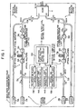
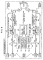
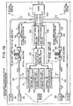
- Fig. 1 is a block diagram showing a configuration of a wavelength division multiplex optical transmission apparatus according to the first embodiment of the present invention.
- a wavelength division multiplex optical transmission apparatus 1 of the embodiment shown in Fig. 1 mainly includes, as an optical sending system 2, optical sending sections (OSs) 2A, 2B, optical fiber type optical amplifies 4A, 4B, and a WDM (Wavelength Division Multiplex) coupler 11, while mainly including, as an optical receiving system 3, optical receiving sections (ORs) 3A, 3B, and optical fiber fusion splice type optical couplers (ODCs) 10A, 10B, and further including an optical output level control section 13.
- ODCs optical fiber fusion splice type optical couplers
- the optical sending section 2A generates, by a laser diode (LD) or the like, an optical signal having a wavelength ⁇ 1 (hereinafter often referred to as send optical signal ⁇ 1) as an optical signal to be sent, and sends the optical signal.
- the optical sending section 2B similarly generates, by a LD or the like, an optical signal having a wavelength ⁇ 3 (hereinafter often referred to as send optical signal ⁇ 3) different from the wavelength ⁇ 1 as an optical signal to be sent, and sends the optical signal.
- optical amplifier (optical amplifying section) 4A is interposed between the optical sending section 2A and the WDM coupler 11 to amplify the send optical signal ⁇ 1 from the optical sending section 2A to a desired optical level.
- optical amplifier (optical amplifying section) 4B is interposed between the optical sending section 2B and the WDM coupler 11 to amplify the send optical signal 3 from the optical sending section 2B to a desired optical level.
- the optical amplifiers 4A, 4B are respectively configured as an erbium-doped fiber type optical amplifier.
- the optical amplifier 4A includes an optical fiber fusion splice type optical coupler 5A (ODC1), optical isolators 6A, 8A, an optical fiber 7A, and an optical band-pass filter 9A.
- the optical amplifier 4B includes an optical fiber fusion splice type optical coupler 5B (ODC3), optical isolators 6B, 8B, an optical fiber 7B, and an optical band-pass filter 9B.
- the optical coupler 5A (5B) processes by wavelength division multiplexing the send optical signal ⁇ 1 ( ⁇ 3) from the optical sending section 2A (2B) and an excitation light signal with a wavelength ⁇ 2 ( ⁇ 3) (hereinafter often referred to as excitation light signal ⁇ 2 2 ( ⁇ 3)) generated in an excitation light source 14A (14B) described infra, thereby adding the excitation light signal ⁇ 2 ( ⁇ 4) to the send optical signal ⁇ 1 ( ⁇ 3).
- the optical fiber 7A (7B) amplifies a gain (optical level) of the send optical signal ⁇ 1 ( ⁇ 3) passing therethrough by the addition of the excitation light signal ⁇ 2 ( ⁇ 4).
- the optical isolators 6A, 8A (6B, 8B) respectively prevent an optical signal [with a wavelength ⁇ 1 + ⁇ 3 ( ⁇ 2 + ⁇ 4)] from the optical coupler 5A (58) from being reflected off I/O portions of the optical fiber 7A (7B).
- the optical isolators 6A, 8A (6B, 8B) can minimize occurrence of noise at the optical fiber 7A (7B), and results in efficient amplification of the send optical signal ⁇ 1 ( ⁇ 3).
- the optical band-pass filter 9A (9B) removes the excitation light signal ⁇ 2 ( ⁇ 4) added through the excitation light source 14A (14B) from the optical signal after the optical amplification, thereby outputting only the send optical signal ⁇ 1 ( ⁇ 3) to an optical transmission line (optical cable) 12 through the WDM coupler 11.
- the optical band-pass filter 9A (9B) also has the function of removing an optical signal with the wavelength ⁇ 1 ( ⁇ 3) input from a reverse direction, thereby preventing the receive optical signal with the wavelength ⁇ 1 ( ⁇ 3) demultiplexed in the WDM coupler 11 as will be described infra from being input into the optical fiber 7A (7B).
- the WDM coupler 11 processes by the wavelength division multiplexing and sends to the optical transmission line 12 the send optical signals ⁇ 1, ⁇ 3 amplified in the optical amplifiers 4A, 4B, while demultiplexing an optical signal transmitted from an opposite side through the optical transmission line 12 into the optical signals with the wavelengths ⁇ 1, ⁇ 3.
- the optical sending system 2 and the optical receiving system 3 share the WDM coupler 11 of the embodiment having both the function as a wavelength division multiplexing section to process by the wavelength division multiplexing and output to the optical transmission line 12 the respective send optical signals ⁇ 1, ⁇ 3 amplified in the optical amplifiers 4A, 4B, and the function as a wavelength division demultiplexing section to demultiplex into the optical signals with the wavelengths ⁇ 1, ⁇ 3 the optical signal processed by the wavelength division multiplexing and transmitted from the opposite side through the optical transmission line 12.
- the optical coupler 10A (10B) causes the receive optical signal ⁇ 1 ( ⁇ 3) demultiplexed in the WDM coupler 11 to branch to the side of the optical sending section 2A (2B) and the side of the optical receiving section 3A (3B) in two directions. Since the receive optical signal ⁇ 1 ( ⁇ 3) branching to the optical sending section 2A (2B) is removed in the optical band-pass filter 9A (9B) as described above, the result is that the receive optical signal ⁇ 1 ( ⁇ 3) branches only to the optical receiving section 3A (3B).
- the optical receiving section 3A receives the optical signal with the wavelength ⁇ 1 from the opposite side, demultiplexed in the WDM coupler 11 to branch at the optical coupler 10A.
- the optical receiving section 3B receives the optical signal with the wavelength ⁇ 3 from the opposite side, demultiplexed in the WDM coupler 11 to branch at the optical coupler 10B.
- the optical signals with the different wavelengths ⁇ 1, ⁇ 3 are processed by the wavelength division multiplexing, and are transmitted through the optical transmission line 12. It is thereby possible to establish bidirectional communication of the optical signals with the wavelengths ⁇ 1, ⁇ 3.
- the above optical output level control section 13 controls optical output levels of the send optical signals ⁇ 1, 3 output to the optical transmission line 12 in the optical sending system 2 for the wavelengths ⁇ 1, ⁇ 3 before the wavelength division multiplexing in the WDM coupler 11.
- individual controls are made to optical levels of the excitation light signals ⁇ 2, ⁇ 4 added to the send optical signals ⁇ 1, ⁇ 3. It is thereby possible to individually vary amplification factors in the optical amplifiers 4A, 4B so as to adjust optical levels of the send optical signals ⁇ 1, ⁇ 2 after the amplification.
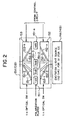
- the optical output level control section 13 of the embodiment includes the excitation light sources 14A, 14B, excitation light output level adjusting sections 15A, 15B, and an excitation light output level control circuit 16A.
- the excitation light source 14A generates the excitation light signal 2 to be added to the send optical signal ⁇ 1 so as to vary the amplification factor in the optical amplifier 4A
- the excitation light source 14B generates the excitation light signal 4 to be added to the send optical signal ⁇ 3 so as to vary the amplification factor in the optical amplifier 4B.
- the excitation light output level adjusting section 15A adjusts the optical output level of the excitation light signal ⁇ 2 generated in the excitation light source 14A
- the excitation light output level adjusting section 15B adjusts the optical output level of the excitation light signal ⁇ 4 generated in the excitation light source 14B.
- the excitation light output level adjusting sections 15A, 15B of the embodiment respectively include a plurality of polarization sections 151-1 to 151-n (where n: natural number more than or equal to 2), and polarization plate selecting optical switches (optical SWs) 152, 153 to select the polarization section 151-i (where i: 1 to n) to pass the excitation light signal ⁇ 2 ( ⁇ 4) therethrough.
- polarization plate selecting optical switches optical SWs
- an optical output port 152-i of the optical switch 152 and an optical input port 153-i of the optical switch 153 are selected in response to a polarization plate selecting signals fed from the excitation light output level control circuit 16A. It is thereby possible to allow the excitation light signal ⁇ 2 ( ⁇ 4) to pass through the selected polarization section 151-i so as to adjust the optical level of the excitation light according to polarization factor thereof.
- the above excitation light output level adjusting sections 15A, 15B each include polarization section 151-I as a polarization section which can vary polarization factors of the excitation light signals ⁇ 2, ⁇ 4 from the excitation light sources 14A, 14B. It is possible to adjust the optical output levels of the excitation light signals ⁇ 2, ⁇ 4 by varying the polarization factors of the polarization section. Moreover, though the polarization factors of the excitation light signals ⁇ 2, ⁇ 4 are varied by respectively selecting any one of the plurality of polarization sections 151-i having the different polarization factors in the discussion, it is to be noted that any other methods may be employed to vary the polarization factors of the excitation light signals ⁇ 2, ⁇ 4.
- the excitation light output level control circuit (excitation light output level operation control section) 16A finds optimal optical output levels of the respective send optical signals ⁇ 1, ⁇ 3 according to transmission distances (characteristics) of the send optical signals ⁇ 1, ⁇ 3 generated in the optical sending sections 2A, 2B, and controls the excitation light output level adjusting sections 15A, 15B (polarization plate selecting optical switches 152, 153) according to the optimal optical output levels so as to respectively adjust the optical output levels of the excitation light signals ⁇ 2, ⁇ 4.
- the excitation light output level control circuit 16A is configured as a polarization plate selecting optical switch control circuit.
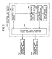
- the excitation light output level control circuit 16A of the embodiment includes a parameter input section 161, an optimal excitation light level calculating section 162, an optimal excitation light level decision section 163, an amplification factor database 164, and an excitation light adjusting signal generating section 165.
- the parameter input section 161 takes as inputs predetermined parameter information about the optical transmission line 12, containing at least information about the transmission distances of the respective send optical signals ⁇ 1, ⁇ 3 to be output to the optical transmission line 12 through a maintenance terminal or the like.
- the following parameter information (1) to (11) are input:
- the optimal excitation light level calculating section (optimal optical output level operation section) 162 finds optimal optical output levels (optical levels after amplification) P of the respective send optical signals ⁇ 1, ⁇ 3 according to the transmission distances of the optical signals having the wavelengths ⁇ 1, ⁇ 3 depending upon the parameter information input through the above parameter input section 161 by arithmetic operation shown by the following expression (1):
- Optimal optical output level P Transmission distance L x (Cable loss Lo + Splice number N x Splice loss Ls) + Optimal receive level Pr + (System margin M + Connector loss Lc + Power penalty D)] where the optimal receive level Pr is set as an intermediate value between the maximum receive level Prmax and the minimum receive level Prmin. That is, the optimal receive level Pr can be found by the following expression (2):
- Optimal receive level Pr (Maximum receive level Prmax + Minimum receive level Prmin)/2
- Optimal optical output level P' Transmission distance L x (Cable loss Lo + Splice number N x Splice loss Ls) + Minimum receive level Prmin + (System margin M + Connector loss Lc + Power penalty D)]
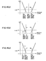
- the minimum receive level Prmin and the maximum receive level Prmax are determined according to a bit error rate (BER) predetermined as a unit standard. For example, when the BER of 1 x 10 -10 is defined as the unit standard, and a relationship as shown in Fig. 4(a) is provided between the optical receive level and the BER, the minimum receive level Prmin corresponds to a position shown by reference numeral 17, and the maximum receive level Prmax corresponds to a position shown by reference numeral 18.
- BER bit error rate
- the optimal receive level Pr is set as the intermediate value between the maximum receive level Prmax and the minimum receive level Prmin. This is because, when the optical receive level exceeds the maximum receive level Prmax or the minimum receive level Prmin, a rapid increase in bit error rate (BER) causes significant deterioration of signal quality as shown in, for example, Figs. 4(b), 4(c).
- BER bit error rate
- the optimal excitation light level decision section 163 makes a decision (determination) of the optical output levels (hereinafter referred to as optimal excitation light levels) of the excitation light signals ⁇ 2, ⁇ 4, which provide optimal values of the amplification factors in the optical amplifiers 4A, 4B depending upon the optimal optical output levels P found by the calculations in the above optimal excitation light level calculating section 162.
- optimal excitation light levels the optical output levels of the excitation light signals ⁇ 2, ⁇ 4
- the optimal excitation light levels are determined by referring to, with the optimal optical output levels P obtained by the above calculations as keys, amplification factor correspondence tables 164a showing relationships between the send optical signal levels in the optical sending sections 2A, 2B, the optical output levels of the excitation light signals ⁇ 2, ⁇ 4, and the optical levels after the amplification.
- the amplification factor database 164 contains the amplification factor correspondence tables 164a respectively corresponding to the wavelengths ⁇ 1, ⁇ 3.
- the excitation light adjusting signal generating section 165 generates excitation light adjusting signals for adjusting the optical output levels of the excitation light signals ⁇ 2, ⁇ 4 depending upon the optimal excitation light levels determined in the optimal excitation light level decision section 163.
- the excitation light level adjusting sections 15A, 15B include the polarization sections 151-i, and the optical switches 152, 153 so that the excitation light adjusting signal generating section 165 generates as the excitation light adjusting signals and feeds to the optical switches 152, 153 polarization plate selecting signals for selecting the polarization sections 151-i to pass the excitation light signals ⁇ 2, ⁇ 4 therethrough.
- the above-mentioned excitation light adjusting signal generating section 165 generates, as the excitation light adjusting signals for the excitation light output level adjusting sections 15A, 15B, polarization factor adjusting signals for adjusting the polarization factors of the polarization section (polarization sections 151-i).
- the excitation light adjusting signal generating section 165 of the embodiment includes an optical switch port decision section 166A, and optical switch control sections 167A, 168A.
- the optical switch port decision section 166A compares excitation light source optical output levels P L input through the above parameter input section 161 with the optimal excitation light levels from the optimal excitation light level decision section 163 so as to find differences therebetween. If there are the differences, the optical switch port decision section 166A decides by how many decibels the current excitation light source optical output levels P L should be increased or decreased in order to set the differences to zeros, and determines polarization plate numbers (optical switch port numbers) corresponding thereto so as to pass the polarization plate numbers to the optical switch control sections 167A, 168A.
- the optical switch control sections 167A, 168A feed to the excitation light level adjusting sections 15A, 15B polarization plate selecting signals for placing in excitation light conducting states the ports 152-i, 153-i of the respective optical switches 152, 153 of the corresponding excitation light level adjusting sections 15A, 15B.
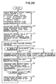
- Step A1 various types of parameter information about the above-mentioned optical transmission line 12 are input into the parameter input section 161 of the excitation light output level control circuit 16A through the maintenance terminal or the like.
- the optimal excitation light level calculating section 162 calculates, depending upon the input parameter information, the optimal optical output levels P for the send optical signals ⁇ 1, ⁇ 3 according to the above expression (1) (Step A2).
- the optimal optical output levels P of the respective send optical signals ⁇ 1, ⁇ 3, obtained in the optimal excitation light level calculating section 162, are fed to the optimal excitation light level decision section 163.
- the optimal excitation light level decision section 163 refers to, with the given optimal optical output levels P as the keys, the amplification factor correspondence tables 164a corresponding to the wavelengths ⁇ 1, ⁇ 3, contained in the amplification factor database 164 (Step A3), and decides whether or not the optimal optical output levels P found by the calculations are appropriate values [whether or not the optimal optical output levels P are present (recorded) in the items "Optical level after amplification"] (Step A4).
- the optimal excitation light level decision section 163 extracts excitation light levels (optimal excitation light levels) corresponding to the optimal optical output levels P (Step A5).
- the optimal optical output levels P are not the appropriate values (if the optimal optical output levels P are not recorded in the amplification factor correspondence tables 164a), for example, optical receive levels cannot be set to intermediate values between the maximum receive levels Prmax and the minimum receive levels Prmin due to, for example, long transmission distances even when the maximum amplification factors are provided in the optical amplifiers 4A, 4B.
- the optimal excitation light level decision section 163 extracts from the amplification factor correspondence tables 164a excitation light levels (maximum excitation light levels) providing the maximum optical levels after amplification so as to set the optical receive levels closer to the intermediate values (from No route in Step A4 to Step A6).
- both the excitation light levels extracted in such a manner are passed to the excitation light adjusting signal generating section 165 as the optimal excitation light levels (Step A7).
- the optical switch port decision section 166A first finds differences between the excitation light output levels P L (current excitation light levels) from the parameter input section 161 and the optimal excitation light levels obtained by the optimal excitation light level decision section 163 as described above (Step A8).
- the optical switch port decision section 166A decides by how many decibels the current excitation light levels should be increased or decreased in order to set the differences to zeros, and selects the polarization plate numbers (optical switch port numbers) corresponding thereto (Step A9) so as to post the polarization plate numbers to the optical switch control sections 167A, 168A.
- the optical switch control sections 167A, 168A generate and feed to the excitation light level adjusting sections 15A, 15B polarization plate selecting signals (electric signals) depending upon the optical switch port numbers from the optical switch port decision section 166A.
- the ports 152-i, 153-i of the respective optical switches 152, 153 are placed in the excitation light conducting states such that excitation lights can pass through the selected polarization sections 151-i (Step A10).
- the respective send optical signals ⁇ 1, ⁇ 3 generated in the respective optical sending sections 2A, 2B are amplified in the optical amplifiers 4A, 4B to the optimal optical output levels according to the transmission distances of the optical signals with the wavelengths ⁇ 1, ⁇ 3, and are sent to the optical transmission line 12.
- the amplification factors in the optical amplifiers 4A, 4B to amplify the send optical signals 11, ⁇ 3 to be sent after the wavelength division multiplexing are individually varied by adjusting the optical output levels of the excitation light signals ⁇ 2, ⁇ 4 added according to the transmission distances (characteristics) of the optical signals with the wavelengths ⁇ 1, ⁇ 3, thereby controlling the optical output levels of the optical signals to the optical transmission line 12 for the wavelengths ⁇ 1, ⁇ 3 (that is, adjusting the optical output levels of the respective send optical signals ⁇ 1, ⁇ 3 for the wavelengths ⁇ 1, ⁇ 3 before the wavelength division multiplexing in the WDM coupler 11). Consequently, it is possible to send the respective send optical signals ⁇ 1, ⁇ 3at the optical output levels most suitable for the optical signals with the wavelengths ⁇ 1, ⁇ 3 with consideration given to the transmission distances of the optical signals with the wavelengths ⁇ 1, ⁇ 3.
- the respective send optical signals ⁇ 1, ⁇ 3 can always be sent at the minimum optical output levels.
- Each optical signal can be sent at the minimum optical output level required for a predetermined optical transmission distance. It is thereby possible to significantly reduce power consumption at a time of optical transmission, and realize the optical transmission at a lower cost.
- the excitation light output level control circuit 16A automatically calculates the optical output levels most suitable for the optical signals with the respective wavelengths ⁇ 1, ⁇ 3 so as to adjust the optical output levels of the excitation light signals ⁇ 2, ⁇ 4 from the excitation light sources 14A, 14B. Therefore, it is possible to extremely easily and accurately adjust the optical output levels of the optical signals with the wavelengths ⁇ 1, ⁇ 3.
- the optical switches 152, 153 of the excitation light output level adjusting sections 15A, 15B are controlled by the electric signals, thereby selecting the polarization sections 151-i to pass the excitation light signals ⁇ 2, ⁇ 4 therethrough.
- the optical switches 152, 153 of the excitation light output level adjusting sections 15A, 15B are controlled by the electric signals, thereby selecting the polarization sections 151-i to pass the excitation light signals ⁇ 2, ⁇ 4 therethrough.
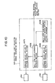
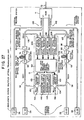
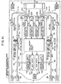
- Fig. 9 is a block diagram showing a configuration of a wavelength division multiplex optical transmission apparatus 1 serving as a first modification of the first embodiment.
- the transmission apparatus 1 shown in Fig. 9 is different from that shown in Fig. 1 in that an optical output level control section 13 includes ball lenses 154 and ceramic devices 155 as excitation light output level adjusting sections 15A, 15B, and an excitation light output level control circuit (ball lens displacing ceramic device control circuit) 16B is provided instead of the excitation light output level control circuit 16A.
- an optical output level control section 13 includes ball lenses 154 and ceramic devices 155 as excitation light output level adjusting sections 15A, 15B
- an excitation light output level control circuit (ball lens displacing ceramic device control circuit) 16B is provided instead of the excitation light output level control circuit 16A.
- the above ball lenses 154 can vary, according to positions of their spherical surfaces on which lights are incident, focus positions (refractive indexes) of the incident lights so as to vary amounts of transmitted lights.
- the ceramic devices 155 move the ball lenses 154 by predetermined amounts in directions away from/closer to the ceramic devices 155 in response to ball lens displacement adjusting signals fed from the ball lens displacing ceramic device control circuit 16B (hereinafter briefly referred to as "ceramic device control circuit 16B").
- Such movements of the ceramic devices 154 vary incident positions of excitation light signals ⁇ 2, ⁇ 4 on the ball lenses 154 to vary focus positions of the excitation light signals ⁇ 2, ⁇ 4 on the ball lenses 154, resulting in varying optical output levels of the excitation light signals ⁇ 2, 4.
- the excitation light output level adjusting sections 15A, 15B respectively include the lenses which can vary the refractive indexes of the passing excitation light signals ⁇ 2, ⁇ 4 according to the incident positions of the excitation light signals ⁇ 2, ⁇ 4 from excitation light sources 14A, 14B.
- the optical output levels of the excitation light signals ⁇ 2, ⁇ 4 can be varied by varying the incident positions of the excitation light signals ⁇ 2, ⁇ 4 on the lenses.
- the ceramic device control circuit 16B finds optimal optical output levels P of respective send optical signals ⁇ 1, ⁇ 3 depending upon various types of parameter information about an optical transmission line 12 to adjust the optical output levels of the excitation light signals 12, ⁇ 4, and has the same configuration as that shown in Fig. 3.
- the excitation light adjusting signal generating section 165 includes a ball lens displacement decision section 166B, ceramic device applied voltage control sections 167B, 168B for the excitation light signals ⁇ 2, ⁇ 4, and a ball lens displacement-ceramic device applied voltage database 169B.
- the ball lens displacement decision section 166B finds positional displacements of the ball lenses 154, required to adjust the optical output levels of the excitation light signals ⁇ 2, ⁇ 4 to optimal excitation light levels obtained in an optimal excitation light level decision section 163 (optimal excitation light level calculating section 162).
- the ball lens displacement decision section 166B refers to, with the positional displacements as keys, the ball lens displacement-ceramic device applied voltage database 169B, thereby determining values of applied voltages to the ceramic devices 155, required to move the ball lenses 154 by the positional displacements.
- the ball lens displacement-ceramic device applied voltage database 169B contains, for each of the send optical signals ⁇ 2, ⁇ 4, a correspondence table (not shown) in which the value of applied voltage to the ceramic device 155 is recorded for each positional displacement of the ball lens 154.
- the ceramic device applied voltage control sections 167B, 168B respectively apply to the ceramic devices 155 voltages according to the ceramic device applied voltage values obtained in the above ball lens displacement decision section 166B.
- the excitation light adjusting signal generating section 165 generates, as excitation light adjusting signals for the excitation light output level adjusting sections 15A, 15B, ball lens displacement adjusting signals (lens incident position adjusting signals) to adjust the incident positions of the excitation light signals ⁇ 2, ⁇ 4 on the ball lenses 154.
- the control circuit 16B first finds by calculations the optimal optical output levels P of the respective send optical signals ⁇ 1, ⁇ 3 depending upon the various types of parameter information about the optical transmission line 12, and determines the optimal excitation light levels according to the obtained optimal optical output levels P so as to pass the optimal excitation light levels to the excitation light adjusting signal generating section 165 (see Steps A1 to A7 in Fig. 7).
- the ball lens displacement decision section 166B finds the positional displacements of the ball lenses 154 corresponding to the optimal excitation light levels input from the optimal excitation light level decision section 163, and refers to the ball lens displacement-ceramic device applied voltage database 169B with the positional displacements as the keys (Step A11).
- the ball lens displacement decision section 166B extracts the values of applied voltages to the ceramic devices 155 for the respective excitation light signals ⁇ 2, ⁇ 4 corresponding to the optimal excitation light level from the above database 169B (Step A12) to post the extracted applied voltage values to the ceramic device applied voltage control sections 167B, 168B.
- the ceramic device applied voltage control sections 167B, 168B respectively apply to the ceramic devices 155 voltages according to the applied voltage values posted from the ball lens displacement decision section 166B, thereby moving the ball lenses 154 to vary the incident positions of excitation light signals ⁇ 2, ⁇ 4 so as to vary the focus positions of the excitation light signals ⁇ 2, ⁇ 4 on the ball lenses 154 (Step A13).
- the optical output levels of the respective excitation light signals ⁇ 2, ⁇ 4 from the excitation light sources 14A, 14B are adjusted to the optimal excitation light levels found by calculations, and the respective send optical signals ⁇ 1, ⁇ 3 are amplified in optical amplifiers 4A, 4B to the optimal optical output levels according to transmission distances of optical signals with the wavelengths ⁇ 1, ⁇ 3, and are sent to the optical transmission line 12.
- the voltages applied to the ceramic devices 155 of the excitation light output level adjusting sections 15A, 15B are controlled to move the ball lenses 154 by the predetermined amounts, thereby varying the focus positions (refractive indexes) of the excitation light signals ⁇ 2, ⁇ 4 on the ball lenses 154. Therefore, it is possible to vary the optical output levels of the excitation light signals ⁇ 2, ⁇ 4 in an analog manner, and adjust the optical output levels of the excitation light signals ⁇ 2, ⁇ 4 more precisely than would be in the above-mentioned first embodiment.
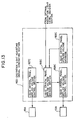
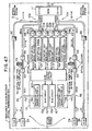
- Fig. 12 is a block diagram showing a configuration of a wavelength division multiplex optical transmission apparatus 1 serving as a second modification of the first embodiment.
- the transmission apparatus 1 shown in Fig. 12 is different from that shown in Fig. 1 in that an optical output level control section 13 includes liquid crystal panels 156 as excitation light output level adjusting sections 15A, 15B, and an excitation light output level control circuit (liquid crystal panel control circuit) 16C is provided instead of the excitation light output level control circuit 16A.
- an optical output level control section 13 includes liquid crystal panels 156 as excitation light output level adjusting sections 15A, 15B
- an excitation light output level control circuit (liquid crystal panel control circuit) 16C is provided instead of the excitation light output level control circuit 16A.
- liquid crystal panels (liquid crystal sections) 156 respectively vary, according to applied voltages, transmission factors of excitation light signals ⁇ 2, ⁇ 4 from excitation light sources 14A, 14B. Variations in applied voltages fed from the liquid crystal panel control circuit 16C vary optical output levels of the excitation light signals ⁇ 2, ⁇ 4.
- the liquid crystal panel control circuit 16C finds optimal optical output levels P of respective send optical signals ⁇ 1, ⁇ 3 depending upon various types of parameter information about an optical transmission line 12 to adjust the optical output levels of the excitation light signals ⁇ 2, ⁇ 4, and has the same configuration as that shown in Fig. 3.
- an excitation light adjusting signal generating section 165 includes a liquid crystal panel applied voltage decision section 166C, liquid crystal panel applied voltage control sections 167C, 168C for the excitation light signals ⁇ 2, ⁇ 4, and a liquid crystal panel applied voltage database 169C.
- the liquid crystal panel applied voltage decision section 166C finds values of applied voltages to the liquid crystal panels 156, required to adjust the optical output levels of the excitation light signals ⁇ 2, ⁇ 4 to optimal excitation light levels obtained in an optimal excitation light level decision section 163 by referring to the liquid crystal panel applied voltage database 169C.
- the liquid crystal panel applied voltage database 169C contains, for each of the send optical signals ⁇ 1, ⁇ 3, a correspondence table (not shown) in which the value of applied voltage to the liquid crystal panel 156 is recorded for each optimal excitation light level.
- liquid crystal panel applied voltage control sections 167C, 168C respectively apply to the liquid crystal panels 156 voltages according to the applied voltage values obtained in the above liquid crystal panel applied voltage decision section 166C.
- the excitation light adjusting signal generating section 165 generates, as excitation light adjusting signals for the excitation light output level adjusting sections 15A, 15B, transmission factor adjusting signals for adjusting the transmission factor of the liquid crystal panel 156.
- the control circuit 16C first finds the optimal optical output levels P of the respective send optical signals 11, ⁇ 3 depending upon the various types of parameter information about the optical transmission line 12, and determines the optimal excitation light levels according to the obtained optimal optical output levels P so as to pass the optimal excitation light levels to the excitation light adjusting signal generating section 165 (see Steps A1 to A7 in Fig. 7).
- the liquid crystal panel applied voltage decision section 166C refers to the liquid crystal panel applied voltage database 169C with the optimal excitation light levels input from the optimal excitation light level decision section 163 as keys (Step A14). Then, the liquid crystal panel applied voltage decision section 166C extracts the values of applied voltages to the liquid crystal panels 156 for the respective excitation light signals ⁇ 2, ⁇ 4 corresponding to the optimal excitation light levels from the above database 169C (Step A15) to post the extracted applied voltage values to the liquid crystal panel applied voltage control sections 167C, 168C.
- liquid crystal panel applied voltage control sections 167C, 168C respectively apply to the liquid crystal panels 156 voltages according to the applied voltage values posted from the liquid crystal panel applied voltage decision section 166C, thereby varying the transmission factor of the liquid crystal panel 156 so as to vary amounts of transmitted lights of the excitation light signals ⁇ 2, ⁇ 4 (Step A16).
- the optical output levels of the respective excitation light signals ⁇ 2, ⁇ 4 from the excitation light sources 14A, 14B are adjusted to the optimal excitation light levels found by the calculations.
- the respective send optical signals ⁇ 1, ⁇ 3 are amplified in optical amplifiers 4A, 4B to the optimal optical output levels according to transmission distances of optical signals with the wavelengths ⁇ 1, ⁇ 3, and are sent to the optical transmission line 12.
- the voltages applied to the liquid crystal panels 156 of the excitation light output level adjusting sections 15A, 15B are varied to adjust the optical output levels of the excitation light signals ⁇ 2, ⁇ 4. Therefore, it is possible to vary the optical output levels of the excitation light signals ⁇ 2, ⁇ 4 in an analog manner, and more precisely adjust the optical output levels of the excitation light signals ⁇ 2, ⁇ 4 in a simpler configuration than would be in the above-mentioned first embodiment.
- Fig. 15 is a block diagram showing a configuration of a wavelength division multiplex optical transmission apparatus 1 serving as a third modification of the first embodiment.
- the transmission apparatus 1 shown in Fig. 15 is different from that shown in Fig. 1 in that an optical output level control section 13 includes bias circuits 157 as excitation light output level adjusting sections 15A, 15B, and an excitation light output level control circuit (bias current control circuit) 16D is provided instead of the excitation light output level control circuit 16A.
- bias circuits 157 respectively vary, according to amounts of fed bias currents, optical levels of excitation light signals ⁇ 2, ⁇ 4 generated in excitation light sources 14A, 14B. Variations in bias currents fed from the bias current control circuit 16D vary values of currents fed to the excitation light sources 14A, 14B to vary the optical output levels of the excitation light signals ⁇ 2, ⁇ 4.
- the bias current control circuit 16D finds optimal optical output levels P of respective send optical signals ⁇ 1, ⁇ 3 depending upon various types of parameter information about an optical transmission line 12 to adjust the optical output levels of the excitation light signals ⁇ 2, ⁇ 4, and has the same configuration as that shown in Fig. 3.
- an excitation light adjusting signal generating section 165 includes a bias current decision section 166D, bias circuit control sections 167D, 168D for the excitation light signals ⁇ 2, ⁇ 4, and a bias current database 169D.
- the bias current decision section 166D determines values of bias currents to the bias circuits 157, required to adjust the optical output levels of the excitation light signals ⁇ 2, ⁇ 4 to optimal excitation light levels obtained by an optimal excitation light level decision section 163 (optimal excitation light level calculation section 162) by referring to the bias current database 169D.
- the bias current database 169D contains, for each of the send optical signals ⁇ 1, ⁇ 3, a correspondence table (not shown) in which the value of voltage applied to the bias circuit 157 is recorded for each optimal excitation light level.
- bias circuit control sections 167D, 168D respectively feed to the bias circuits 157 bias currents according to the bias current values obtained in the above bias current decision section 166D.
- the excitation light adjusting signal generating section 165 generates, as excitation light adjusting signals for the excitation light output level adjusting sections 15A, 15B, bias current adjusting signals for adjusting the amounts of bias currents of the bias circuits 157.
- the control circuit 16D first finds by calculations the optimal optical output levels P of the respective send optical signals ⁇ 1, ⁇ 3 depending upon the various types of parameter information about the optical transmission line 12, and determines the optimal excitation light levels according to the obtained optimal optical output levels P so as to pass the optimal excitation light levels to the excitation light adjusting signal generating section 165 (see Steps A1 to A7 in Fig. 7).
- the bias current decision section 166D refers to the bias current database 169D with the optimal excitation light levels input from the optimal excitation light level decision section 163 as keys (Step A17). Then, the bias current decision section 166D extracts the bias current values fed to the bias circuits 157 for the respective excitation light signals ⁇ 2, ⁇ 4 corresponding to the optimal excitation light levels from the above bias current database 169D (Step A18) to post the extracted bias current values to the bias circuit control sections 167D, 168D.
- the bias circuit control sections 167D, 168D respectively feed to the bias circuits 157 the bias currents according to the bias current values posted from the bias current decision section 166D, thereby varying the amounts of currents fed from the bias circuits 157 to the excitation light sources 14A, 14B so as to vary the optical levels of the excitation light signals ⁇ 2, ⁇ 4 (Step A19).
- the optical output levels of the respective excitation light signals ⁇ 2, ⁇ 4 from the excitation light sources 14A, 14B are adjusted to the optimal excitation light levels found by the calculations.
- the respective send optical signals ⁇ 1, ⁇ 3 are amplified in optical amplifiers 4A, 4B to the optimal optical output levels according to transmission distances of optical signals with the wavelengths ⁇ 1, ⁇ 3, and are sent to the optical transmission line 12.
- the excitation light output level adjusting sections 15A, 15B are configured as the bias circuits 157 which can vary the amounts of currents fed to the excitation light sources 14A, 14B. Therefore, it is possible to vary the optical output levels of the excitation light signals ⁇ 2, ⁇ 4 generated in the excitation light sources 14A, 14B directly and in an analog manner, and adjust the optical output levels of the excitation light signals ⁇ 2, ⁇ 4 more accurately and more precisely than would be in the first embodiment.
- the above-mentioned method of adjusting the optical output levels of the send optical signals ⁇ 1, ⁇ 3 (the optical output levels of the excitation light signals ⁇ 2, ⁇ 4) is applied to the transmission apparatus 1 including both the optical sending system 2 and the optical receiving system 3.
- the method of adjusting may similarly be applied to any transmission apparatus as long as it has at least the optical sending system 2.
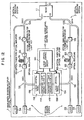
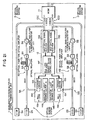
- Fig. 18 is a block diagram showing a configuration of a wavelength division multiplex optical transmission apparatus 1 serving as the second embodiment of the present invention.
- the transmission apparatus 1 shown in Fig. 18 is different from that shown in Fig. 1 in that one-to-three optical couplers 10C, 10D are provided to cause respective receive optical signals ⁇ 1, ⁇ 3 split in a WDM coupler 11 to additionally branch to an optical output level control section 13 instead of the optical couplers 10A, 10B, and the optical output level control section 13 includes an excitation light output level control circuit (polarization plate selecting optical switch control circuit) 16E instead of the excitation light output level control circuit (polarization plate selecting optical switch control circuit) 16A, and input optical signal receivers 19A, 19B.
- excitation light level adjusting sections 15A, 15B respectively include polarization sections 151-i, and optical switches 152, 153 as in those shown in Fig. 2.
- the above input optical signal receiver (input signal light receiving section) 19A receives the receive optical signal ⁇ 1 which is transmitted from an opposite side through an optical transmission line 12 to be demultiplexed in the WDM coupler 11, and is subsequently caused to branch at the optical coupler 10A.
- the input optical signal receiver 19B similarly receives the receive optical signal ⁇ 3 demultiplexed in the WDM coupler 11, and is subsequently caused to branch at the optical coupler 10B.
- the excitation light output level control circuit (excitation light output level operation control section) 16E finds optimal optical output levels P according to transmission distances (characteristics) of optical signals with the wavelengths ⁇ 1, ⁇ 3, and controls the excitation light output level adjusting sections 15A, 15B according to the optimal optical output levels P to adjust optical output levels of excitation light signals ⁇ 2, ⁇ 4.
- the optimal optical output levels P are found depending upon the optical levels of the receive optical signals ⁇ 1, ⁇ 3 from the opposite side, received in the above input optical signal receivers 19A, 19B.
- the excitation light output level control circuit 16E of the second embodiment includes an optimal excitation light level decision section 163, an amplification factor database 164, and an excitation light adjusting signal generating section 165 identical with those in the first embodiment, and further includes an optical level input section 171, a transmission loss calculating section 172, and an optimal excitation light level calculating section 173.
- the excitation light adjusting signal generating section 165 of the embodiment has an optical switch port decision section 166A, and optical switch control sections 167A, 168A identical with those shown in Fig. 6.
- the optical level input section 171 takes as inputs various types of optical levels such as output signal optical level P S at the opposite side, local excitation light output level P L , minimum receive level Prmin, and maximum receive level Prmax.
- the transmission loss calculating section (transmission loss operation section) 172 finds actual transmission losses (transmission loss information) P Loss of the wavelengths ⁇ 1, ⁇ 3 actually transmitted from the opposite side through the optical transmission line 12 for a predetermined transmission distance depending upon the optical signals with the wavelengths ⁇ 1, ⁇ 3 received in the input optical signal receivers 19A, 19B.
- the actual transmission losses P LOSS are found by subtracting the output signal optical levels P s at the opposite side from receive levels Pr' of the optical signals with the wavelengths ⁇ 1, ⁇ 3 received in the input signal receivers 19A, 19B.
- the optimal excitation light level calculating section (optimal optical output level operation section) 173 finds according to predetermined arithmetic operations optimal optical output levels P of the optical signals with the wavelengths ⁇ 1, ⁇ 3 depending upon the actual transmission losses P Loss obtained in the transmission loss calculating section 172.
- the optimal optical output levels P are found for the send optical signals ⁇ 1, ⁇ 3 with consideration given to the actual transmission losses of the send optical signals ⁇ 1, ⁇ 3 due to states (such as loss) of the optical transmission line 12 so as to adjust the optical output levels of the excitation light signals ⁇ 2, ⁇ 4 generated in the excitation light sources 14A, 14B according to the optimal optical output levels P.
- Steps B1 to B8 shown in Fig. 20, a detailed description will now be given of an operation of the wavelength division multiplex optical transmission apparatus 1 of the second embodiment having the above configuration with attention to excitation light output level adjusting processing.
- the optical level input section 171 of the excitation light output level control circuit 16E takes as inputs the various types of optical levels described above (such as output signal optical level P S at the opposite side, local excitation light output level P L , minimum receive level Prmin, and maximum receive level Prmax) through a maintenance terminal (Step B1).
- the transmission loss calculating section 172 finds the actual transmission losses P LOSS of the wavelengths ⁇ 1, ⁇ 3 by subtracting the output optical levels P S at the opposite side from the receive levels Pr' of the optical signals with the wavelengths ⁇ 1, ⁇ 3 received in the input optical signal receivers 19A, 19B (Step B2).
- the obtained actual transmission losses P Loss are passed to the optimal excitation light level calculating section 173.
- the optimal optical output levels P of the respective send optical signals ⁇ 1, ⁇ 3 obtained in such a manner are given to the optimal excitation light level decision section 163.
- the optimal excitation light level decision section 163 refers to, with the given optimal optical output levels P as keys, amplification factor correspondence tables 164a (see Fig. 5) contained in the amplification factor database 164 to correspond to the wavelengths ⁇ 1, ⁇ 3 (Step B4), and decides whether or not the obtained optimal optical output levels P are appropriate values [whether or not the optimal optical output levels P are present (recorded) in the items "Optical level after amplification"] (Step B5).
- the optimal excitation light level decision section 163 extracts excitation light levels (optimal excitation light levels) corresponding to the optimal optical output levels P (Step B6).
- the optimal excitation light level decision section 163 extracts excitation light levels (maximum excitation light levels) providing the maximum optical levels after amplification from the amplification factor correspondence tables 164a so as to set the optical receive levels closer to the intermediate values (from No route in Step B5 to Step B7).
- both the excitation light levels extracted in such a manner are passed to the excitation light adjusting signal generating section 165 as the optimal excitation light levels (Step B8).
- the excitation light adjusting signal generating section 165 selects the polarization sections 151-i to pass the excitation light signals ⁇ 1, ⁇ 3 therethrough, and controls the optical switches 152, 153 such that the excitation light signals ⁇ 1, ⁇ 3 can pass through the selected polarization sections 151-i (see Steps A8 to A10 in Fig. 8).
- the respective send optical signals ⁇ 1, ⁇ 3 are amplified in the optical amplifiers 4A, 4B to the optimal optical output levels according to the transmission distances of the optical signals with the wavelengths ⁇ 1, ⁇ 3 and the loss of the optical transmission line 12, and are sent to the optical transmission line 12.
- the optimal optical output levels P for the respective send optical signals ⁇ 1, ⁇ 3 are found according to the arithmetic operations depending upon the actual transmission losses P Loss of the optical signals with the wavelengths ⁇ 1, ⁇ 3 actually transmitted through the optical transmission line 12.
- the optical output levels of the respective excitation light signals ⁇ 2, ⁇ 4 are adjusted depending upon the obtained optimal optical output levels P. Consequently, it is possible to adjust the optical output levels of the send optical signals ⁇ 1, ⁇ 3 with consideration given to the actual state (such as loss) of the optical transmission line 12, and adjust the optical output levels of the send optical signals ⁇ 1, ⁇ 3 to the optimal values more accurately than would be in the first embodiment.
- the optical output levels of the excitation light signals ⁇ 2, ⁇ 4 generated in the respective excitation light sources 14A, 14B are adjusted by the polarization sections 151-i, and the optical switches 152, 153.
- the optical levels of the send optical signals ⁇ 1, ⁇ 3 after the optical amplification are adjusted by the polarization sections 151-i, and the optical switches 152, 153.
- Fig. 21 is a block diagram showing a configuration of a wavelength division multiplex optical transmission apparatus 1 serving as a first modification of the second embodiment.
- the transmission apparatus 1 shown in Fig. 21 is different from that shown in Fig. 18 in that excitation light output level adjusting sections 15A, 15B are respectively configured by using the ball lenses 154 and the ceramic devices 155 described in the above first modification (see Fig. 9) of the first embodiment, and an excitation light output level control circuit (ball lens displacing ceramic device control circuit) 16F is provided instead of the excitation light output level control circuit 16E.
- excitation light output level control circuit ball lens displacing ceramic device control circuit
- an excitation light adjusting signal generating section 165 includes a ball lens displacement decision section 166B, ceramic device applied voltage control sections 167B, 168B, and a ball lens displacement-ceramic device applied voltage database 169B identical with those shown in Fig. 10.
- the optical output levels of the excitation light signals ⁇ 2, ⁇ 4 generated in the respective excitation light sources 14A, 14B are respectively adjusted by the ball lenses 154 and the ceramic devices 155 in an optical output level control section 13 of the type finding optimal optical output levels P of respective send optical signals ⁇ 1, ⁇ 3 by the arithmetic operations depending upon actual transmission losses P LOSS of wavelengths ⁇ 1, ⁇ 3.
- Step B8 described above referring to Fig. 20 excitation light output level adjusting processing of the transmission apparatus 1 in the modification is identical with the processing from Steps A11 to A13 described above referring to Fig. 11. That is, the control circuit 16F first finds the optimal optical output levels P with consideration given to the actual transmission losses P LOSS of the optical signals with the wavelengths ⁇ 1, ⁇ 3, and determines the optimal excitation light levels according to the obtained optimal optical output levels P to pass the optimal excitation light levels to the excitation light adjusting signal generating section 165 (see Steps B1 to B8 in Fig. 20).
- the excitation light adjusting signal generating section 165 finds positional displacements of the ball lenses 154, corresponding to the optimal excitation light levels input from the optimal excitation light level decision section 163.
- the positional displacements are converted into values of applied voltages to the ceramic devices 155, and the voltages are applied to the ceramic devices 155.
- This varies focus positions of the excitation light signals ⁇ 2, ⁇ 4 on the ball lenses 154 to adjust the optical output levels of the respective excitation light signals ⁇ 2, ⁇ 4 from the excitation light sources 14A, 14B to the above optimal excitation light levels (see Steps A11 to A13 in Fig. 11).
- the respective send optical signals ⁇ 1, ⁇ 3 are amplified in the optical amplifiers 4A, 4B to the optimal optical output levels according to transmission distances of the optical signals with the respective wavelengths ⁇ 1, ⁇ 3 and a loss of an optical transmission line 12, and are sent to the optical transmission line 12.
- the controls of the applied voltages to the ceramic devices 155 of the excitation light output level adjusting sections 15A, 15B vary the focus positions (refractive indexes) of the excitation light signals ⁇ 2, ⁇ 4 on the ball lenses 154. Therefore, it is possible to vary the optical output levels of the excitation light signals ⁇ 2, ⁇ 4 in an analog manner, and adjust the optical output levels of the excitation light signals ⁇ 2, ⁇ 4 more precisely than would be in the above-mentioned second embodiment.
- Fig. 22 is a block diagram showing a configuration of a wavelength division multiplex optical transmission apparatus 1 serving as a second modification of the second embodiment.
- the transmission apparatus 1 shown in Fig. 22 is different from that shown in Fig. 18 in that excitation light output level adjusting sections 15A, 15B are respectively configured by using the liquid crystal panels 156 described in the second modification (see Fig. 12) of the first embodiment, and an excitation light output level control circuit (liquid crystal panel control circuit) 16G is provided instead of the excitation light output level control circuit 16E.
- excitation light output level control circuit liquid crystal panel control circuit
- an excitation light adjusting signal generating section 165 includes a liquid crystal panel applied voltage decision section 166C, liquid crystal panel applied voltage control sections 167C, 168C, and a liquid crystal panel applied voltage database 169C identical with those shown in Fig. 13.
- the optical output levels of the excitation light signals ⁇ 2, ⁇ 4 generated in the respective excitation light sources 14A, 14B are respectively adjusted by the liquid crystal panels 156 in an optical output level control section 13 of the type finding optimal optical output levels P of respective send optical signals ⁇ 1, ⁇ 3 by arithmetic operations depending upon actual transmission losses P LOSS of wavelengths ⁇ 1, ⁇ 3.
- Step B8 described above referring to Fig. 20 excitation light output level adjusting processing of the transmission apparatus 1 in the modification is identical with the processing from Steps A14 to A16 described above referring to Fig. 14. That is, the control circuit 16G first finds the optimal optical output levels P with consideration given to the actual transmission losses P Loss of the optical signals with the wavelengths ⁇ 1, ⁇ 3, and determines the optimal excitation light levels according to the obtained optimal optical output levels P to pass the optimal excitation light levels to the excitation light adjusting signal generating section 165 (see Steps B1 to B8 in Fig. 20).
- the excitation light adjusting signal generating section 165 finds applied voltages to the liquid crystal panels 156, corresponding to the optimal excitation light levels input from the optimal excitation light level decision section 163 so as to apply the applied voltages to the respective liquid crystal panels 156. This varies light transmittances of the liquid crystal panels to adjust the optical output levels of the excitation light signals ⁇ 2, ⁇ 4 from the excitation light sources 14A, 14B to the above optimal excitation light levels (see Steps A14 to A16 in Fig. 14).
- the respective send optical signals ⁇ 1, ⁇ 3 are amplified in the optical amplifiers 4A, 4B to the optimal optical output levels according to transmission distances of the optical signals with the respective wavelengths ⁇ 1, ⁇ 3 and a loss of an optical transmission line 12, and are sent to the optical transmission line 12.
- the variations in voltages applied to the liquid crystal panels 156 of the excitation light output level adjusting sections 15A, 15B can adjust the optical output levels of the excitation light signals ⁇ 2, ⁇ 4. Therefore, it is possible to vary the optical output levels of the excitation light signals ⁇ 2, ⁇ 4 in an analog manner, and adjust the optical output levels of the excitation light signals ⁇ 2, ⁇ 4 more precisely in a simpler configuration than would be in the above-mentioned second embodiment.
- Fig. 23 is a block diagram showing a configuration of a wavelength division multiplex optical transmission apparatus 1 serving as a third modification of the second embodiment.
- the transmission apparatus 1 shown in Fig. 23 is different from that shown in Fig. 18 in that excitation light output level adjusting sections 15A, 15B are respectively configured by using the bias circuits 157 described in the third modification (see Fig. 15) of the first embodiment, and an excitation light output level control circuit (bias current control circuit) 16H is provided instead of the excitation light output level control circuit 16E.
- bias current control circuit bias current control circuit
- an excitation light adjusting signal generating section 165 includes a bias current decision section 166D, bias circuit control sections 167D, 168D, and a bias current database 169D identical with those shown in Fig. 16.
- the optical output levels of the excitation light signals ⁇ 2, ⁇ 4 generated in the excitation light sources 14A, 14B are respectively adjusted by the bias circuits 157 in an optical output level control section 13 of the type finding optimal optical output levels P of respective send optical signals ⁇ 1, ⁇ 3 by arithmetic operations depending upon actual transmission losses P LOSS of wavelengths ⁇ 1, ⁇ 3.
- Step B8 described above referring to Fig. 20 excitation light output level adjusting processing of the transmission apparatus 1 in the modification is identical with the processing from Steps A17 to A19 described above referring to Fig. 17. That is, the control circuit 16H first finds the optimal optical output levels P with consideration given to the actual transmission losses P Loss of the optical signals with the wavelengths ⁇ 1, ⁇ 3, and determines the optimal excitation light levels according to the obtained optimal optical output levels P so as to pass the optimal excitation light levels to the excitation light adjusting signal generating section 165 (see Steps B1 to B8 in Fig. 20).
- the excitation light adjusting signal generating section 165 finds values of bias currents to the bias circuits 157, corresponding to the optimal excitation light levels input from the optimal excitation light level decision section 163 so as to feed the bias currents to the respective bias circuits 157. This varies amounts of bias currents from the bias circuits 157 to the respective excitation light sources 14A, 14B, thereby adjusting the optical output levels of the excitation light signals ⁇ 2, ⁇ 4 generated in the excitation light sources 14A, 14B to the above optimal excitation light levels (see Steps A17 to A19 in Fig. 17).
- the respective send optical signals ⁇ 1, ⁇ 3 are amplified in the optical amplifiers 4A, 4B to the optimal optical output levels according to transmission distances of the optical signals with the respective wavelengths ⁇ 1, ⁇ 3 and a loss of an optical transmission line 12, and are sent to the optical transmission line 12.
- the excitation light output level adjusting sections 15A, 15B are respectively configured as the bias circuits 157 which can vary the amounts of currents fed to the excitation light sources 14A, 14B. Therefore, it is possible to vary the optical output levels of the excitation light signals ⁇ 2, ⁇ 4 generated in the excitation light sources 14A, 14B directly and in an analog manner, and adjust the optical output levels of the excitation light signals ⁇ 2, ⁇ 4 more accurately and more precisely than would be in the second embodiment.
- Fig. 24 is a block diagram showing a configuration of a wavelength division multiplex optical transmission apparatus 1 serving as the third embodiment of the present invention.
- the transmission apparatus 1 shown in Fig. 24 is different from that shown in Fig. 18 of the second embodiment in that optical couplers 10E, 10F are mounted to output terminals of respective optical amplifiers 4A, 4B, and an optical output level control section 13 includes an excitation light output level control circuit (polarization plate selecting optical switch control circuit) 16J instead of the excitation light output level control circuit (polarization plate selecting optical switch control circuit) 16E, and output optical signal receivers 20A, 20B.
- excitation light output level adjusting sections 15A, 15B respectively include polarization sections 151-i, and optical switches 152, 153 as in those shown in Fig. 2.
- the above optical couplers 10E, 10F cause send optical signals ⁇ 1, ⁇ 3 respectively amplified in the optical amplifiers 4A, 4B to branch to the side of a WDM coupler 11 and the side of the optical output level control section 13.
- the output optical signal receivers (output signal light receiving sections) 20A, 20B respectively receive the receive optical signals ⁇ 1, ⁇ 3 caused to branch at the corresponding optical couplers 10E, 10F (parts of the respective send optical signals ⁇ 1, ⁇ 3 to be output to an optical transmission line 12 through the WDM coupler 11 after amplification in the optical amplifiers 4A, 4B).
- the excitation light output level control circuit (excitation light output level operation control section) 16J finds optimal optical output levels P according to transmission distances (characteristics) of optical signals with wavelengths ⁇ 1, ⁇ 3 with consideration given to actual transmission losses P LOSS of the optical signals with the respective wavelengths ⁇ 1, ⁇ 3, and controls the excitation light output level adjusting sections 15A, 15B according to the optimal optical output levels P to adjust optical output levels of excitation light signals ⁇ 2, ⁇ 4.
- the optimal optical output levels P are corrected depending upon the optical levels of the send optical signals ⁇ 1, ⁇ 3 after the optical amplification, received in the above output optical signal receivers 20A, 20B.
- the excitation light output level control circuit 16J of the third embodiment includes an optical level input section 171, a transmission loss calculating section 172, and an optimal excitation light level calculating section 173 identical with those described in the second embodiment, an optimal excitation light level decision section 163, an amplification factor database 164, and an excitation light adjusting signal generating section 165 identical with those described in the first embodiment, and further includes a level comparing section 174, and a level correcting section 175.
- the excitation light adjusting signal generating section 165 of the embodiment includes an optical switch port decision section 166A, and optical switch control sections 167A, 168A identical with those shown in Fig. 6.
- the above level comparing section 174 compares the optimal optical output levels P of the respective send optical signals ⁇ 1, ⁇ 3, calculated in the optimal excitation light level calculating section 173 with optical levels of the send optical signals ⁇ 1, ⁇ 3 after actual optical amplification, respectively received in the output optical signal receivers 20A, 20B. If errors are caused between the above optical levels as a result of comparison in the level comparing section 174, the level correcting section 175 causes the optimal excitation light level calculating section 173 to recalculate the optimal optical output level P so as to minimize the errors, resulting in correcting generation processing for the excitation light adjusting signals in the excitation light adjusting signal generating section 165.
- the optical output level control section 13 of the third embodiment monitors whether or not the optical levels of the send optical signals ⁇ 1, ⁇ 3 after optical amplification actually become the optimal optical output levels P by the output optical signal receivers 20A, 20B receiving the parts of the send optical signals ⁇ 1, ⁇ 3 after optical amplification. If the optical levels of the send optical signals ⁇ 1, ⁇ 3 after optical amplification are deviated from the optimal optical output levels P obtained according the calculations, the optical output level control section 13 corrects the deviations.
- Steps C1 to C11 Referring to the flowchart (Steps C1 to C11) shown in Fig. 26, a detailed description will now be given of an operation of the wavelength division multiplex optical transmission apparatus 1 of the third embodiment having the above configuration with attention to excitation light output level adjusting processing.
- processing in Steps C1 to C8 are identical with those in Steps B1 to B8 described above referring to Fig. 20 of the second embodiment, and descriptions thereof are omitted.
- a description will be directed to processing after the excitation light adjusting signal generation processing (that is, after the optical output levels of the excitation light signals ⁇ 2, ⁇ 4 are adjusted to the optimal excitation light levels).
- the excitation light adjusting signal generating section 165 generates excitation light adjusting signals to respectively control the excitation light output level adjusting sections 15A, 15B so as to adjust the optical output levels of the excitation light signals ⁇ 2, ⁇ 4 to the optimal excitation light levels (Step C8).
- the level comparing section 174 compares the optimal optical output levels P for the respective wavelengths ⁇ 1, ⁇ 3, found in the optimal excitation light level calculating section 173 with optical levels of the send optical signals ⁇ 1, ⁇ 3 after optical amplification, received in the output optical signal receivers 20A, 20B (Step C9).
- the level correcting section 175 instructs the optimal excitation light level calculating section 173 to recalculate the optimal optical output levels P, thereby causing the optimal excitation light level calculating section 173 to recalculate the optimal optical output levels P so as to set the respective optical level errors to zeros (Step C11).
- the optimal optical output levels P found by the recalculations are passed to the optimal excitation light level decision section 163 once again, and the optimal excitation light level decision section 163 extracts the optimal excitation light levels corresponding to the optimal optical output levels P from amplification factor correspondence tables 164a (see Fig. 5) of the amplification factor database 164 to output the extracted optimal excitation light levels to the excitation light adjusting signal generating section 165 (Step C8).
- the excitation light adjusting signal generating section 165 reselects the polarization sections 151-i to pass the excitation light signals ⁇ 1, ⁇ 3 therethrough, and controls the optical switches 152, 153 such that the excitation light signals ⁇ 1, ⁇ 3 can pass through the polarization sections 151-i (see Steps A8 to A10 in Fig. 8).
- This corrects the optical output levels of the respective excitation light signals ⁇ 2, ⁇ 4 generated in the respective excitation light sources 14A, 14B.
- the respective send optical signals ⁇ 1, ⁇ 3 are sent to the optical transmission line 12 at the corrected optimal optical output levels.
- the wavelength division multiplex optical transmission apparatus 1 of the third embodiment if the errors are caused between the optimal optical output levels P found by the calculations and the optical levels of the send optical signals ⁇ 1, ⁇ 3 after optical amplification, adjustments of the excitation light levels are corrected so as to set the errors to zeros. Consequently, even when the optical levels of the respective send optical signals ⁇ 1, ⁇ 3 are varied due to the characteristics of the optical amplifiers 4A, 4B, disturbance, and so forth, it is possible to continuously stabilize the optical levels of the respective send optical signals ⁇ 1, ⁇ 3 at the optimal levels while following the variations. Thus, it is possible to provide an advantage of significantly enhanced performance of the transmission apparatus 1 as well as the same advantages as those in the second embodiment.
- the optical switches 152, 153 of the excitation light output level adjusting sections 15A, 15B are controlled by the electric signals, thereby selecting the polarization sections 151-i to pass the excitation light signals ⁇ 2, ⁇ 4 therethrough.
- the optical switches 152, 153 of the excitation light output level adjusting sections 15A, 15B are controlled by the electric signals, thereby selecting the polarization sections 151-i to pass the excitation light signals ⁇ 2, ⁇ 4 therethrough.
- Fig. 27 is a block diagram showing a configuration of a wavelength division multiplex optical transmission apparatus 1 serving as a first modification of the third embodiment.
- the transmission apparatus 1 shown in Fig. 27 is different from that shown in Fig. 24 in that excitation light output level adjusting sections 15A, 15B are respectively configured by using the ball lenses 154 and the ceramic devices 155 described in the above first modification (see Fig. 9) of the first embodiment, and an excitation light output level control circuit (ball lens displacing ceramic device control circuit) 16K is provided instead of the excitation light output level control circuit 16J.
- excitation light output level control circuit ball lens displacing ceramic device control circuit
- an excitation light adjusting signal generating section 165 includes a ball lens displacement decision section 166B, ceramic device applied voltage control sections 167B, 168B, and a ball lens displacement-ceramic device applied voltage database 169B identical with those shown in Fig. 10.
- optical output levels of excitation light signals ⁇ 2, ⁇ 4 generated in the excitation light sources 14A, 14B are respectively adjusted by the ball lenses 154 and the ceramic devices 155 in an optical output level control section 13 of the type correcting optimal optical output levels P calculated depending upon actual transmission losses P LOSS of wavelengths ⁇ 1, ⁇ 3 according to optical levels of send optical signals ⁇ 1, ⁇ 3 after actual optical amplification.
- Step C8 described above referring to Fig. 26 excitation light output level adjusting processing of the transmission apparatus 1 in the modification is identical with the processing from Steps A11 to A13 described above referring to Fig. 11. That is, the control circuit 16K first finds the optimal optical output levels P with consideration given to the actual transmission losses P Loss of the optical signals with the wavelengths ⁇ 1, ⁇ 3, and determines optimal excitation light levels according to the obtained optimal optical output levels P so as to pass the optimal excitation light levels to the excitation light adjusting signal generating section 165 (see Steps C1 to C8 in Fig. 25).
- the excitation light adjusting signal generating section 165 finds positional displacements of the ball lenses 154, corresponding to the optimal excitation light levels input from the optimal excitation light level decision section 163.
- the positional displacements are converted into values of applied voltages to the ceramic devices 155, and the voltages are applied to the ceramic devices 155.
- This varies focus positions of the excitation light signals ⁇ 2, ⁇ 4 on the ball lenses 154 to adjust the optical output levels of the respective excitation light signals ⁇ 2, ⁇ 4 from the excitation light sources 14A, 14B to the above optimal excitation light levels (see Steps A11 to A13 in Fig. 11).
- the respective send optical signals ⁇ 1, ⁇ 3 are amplified in the optical amplifiers 4A, 4B to the optimal optical output levels according to transmission distances of the optical signals with the respective wavelengths ⁇ 1, ⁇ 3 and a loss of an optical transmission line 12, and are sent to the optical transmission line 12.
- the optimal optical output levels P are recalculated in the optimal excitation light level calculating section 173 so as to set the errors to zeros, thereby correcting the optimal excitation light levels (see Steps C10, C11 in Fig. 26).
- the controls of the voltages applied to the ceramic devices 155 of the excitation light output level adjusting sections 15A, 15B vary the focus positions (refractive indexes) of the excitation light signals ⁇ 2, ⁇ 4 on the ball lenses 154. Therefore, it is possible to vary the optical output levels of the excitation light signals ⁇ 2, ⁇ 4 in an analog manner, and adjust the optical output levels of the excitation light signals ⁇ 2, ⁇ 4 more precisely than would be in the above-mentioned third embodiment.
- Fig. 28 is a block diagram showing a configuration of a wavelength division multiplex optical transmission apparatus 1 serving as a second modification of the third embodiment.
- the transmission apparatus 1 shown in Fig. 28 is different from that shown in Fig. 24 in that excitation light output level adjusting sections 15A, 15B are respectively configured by using the liquid crystal panels 156 described in the second modification (see Fig. 12) of the first embodiment, and an excitation light output level control circuit (liquid crystal panel control circuit) 16L is provided instead of the excitation light output level control circuit 16J.
- excitation light output level control circuit liquid crystal panel control circuit
- an excitation light adjusting signal generating section 165 includes a liquid crystal panel applied voltage decision section 166C, liquid crystal panel applied voltage control sections 167C, 168C, and a liquid crystal panel applied voltage database 169C identical with those shown in Fig. 13.
- optical output levels of excitation light signals ⁇ 2, ⁇ 4 generated in the excitation light sources 14A, 14B are respectively adjusted by the liquid crystal panels 156 in an optical output level control section 13 of the type correcting optimal optical output levels P calculated depending upon actual transmission losses P LOSS of wavelengths ⁇ 1, ⁇ 3 according to optical levels of send optical signals ⁇ 1, ⁇ 3 after actual optical amplification.
- excitation light output level adjusting processing of the transmission apparatus 1 in the modification is identical with the processing from Steps A14 to A16 described above referring to Fig. 14. That is, the control circuit 16L first finds the optimal optical output levels P with consideration given to the actual transmission losses P Loss of the optical signals with the respective wavelengths ⁇ 1, ⁇ 3, and determines optimal excitation light levels according to the obtained optimal optical output levels P so as to pass the optimal excitation light levels to the excitation light adjusting signal generating section 165 (see Steps C1 to C8 in Fig. 26).
- the excitation light adjusting signal generating section 165 finds applied voltages to the liquid crystal panels 156, corresponding to the optimal excitation light levels input from the optimal excitation light level decision section 163 so as to apply the applied voltages to the respective liquid crystal panels 156. This varies light transmittances of the liquid crystal panels to adjust the optical output levels of the excitation light signals ⁇ 2, ⁇ 4 from the excitation light sources 14A, 14B to the above optimal excitation light levels (see Steps A14 to A16 in Fig. 14).
- the respective send optical signals ⁇ 1, ⁇ 3 are amplified in the optical amplifiers 4A, 4B to the optimal optical output levels according to transmission distances of the optical signals with the respective wavelengths ⁇ 1, ⁇ 3 and a loss of an optical transmission line 12, and are sent to the optical transmission line 12.
- the optimal optical output levels P are recalculated in the optimal excitation light level calculating section 173 so as to set the errors to zeros, thereby correcting the optimal excitation light levels (see Steps C10, C11 in Fig. 26).
- the variations in voltages applied to the liquid crystal panels 156 of the excitation light output level adjusting sections 15A, 15B can adjust the optical output levels of the excitation light signals ⁇ 2, ⁇ 4. Therefore, it is possible to vary the optical output levels of the excitation light signals ⁇ 2, ⁇ 4 in an analog manner, and adjust the optical output levels of the excitation light signals ⁇ 2, ⁇ 4 more precisely in a simpler configuration than would be in the above-mentioned third embodiment.
- Fig. 29 is a block diagram showing a configuration of a wavelength division multiplex optical transmission apparatus 1 serving as a third modification of the third embodiment.
- the transmission apparatus 1 shown in Fig. 29 is different from that shown in Fig. 24 in that excitation light output level adjusting sections 15A, 15B are respectively configured by using the bias circuits 157 described in the third modification (see Fig. 15) of the first embodiment, and an excitation light output level control circuit (bias current control circuit) 16M is provided instead of the excitation light output level control circuit 16J.
- bias current control circuit bias current control circuit
- an excitation light adjusting signal generating section 165 includes a bias current decision section 166D, bias circuit control sections 167D, 168D, and a bias current database 169D identical with those shown in Fig. 16.
- optical output levels of excitation light signals ⁇ 2, ⁇ 4 generated in the excitation light sources 14A, 14B are respectively adjusted by the bias circuits 157 in an optical output level control section 13 of the type correcting optimal optical output levels P calculated depending upon actual transmission losses P Loss of wavelengths ⁇ 1, ⁇ 3 according to optical levels of send optical signals ⁇ 1, ⁇ 3 after actual optical amplification.
- excitation light output level adjusting processing of the transmission apparatus 1 in the modification is identical with the processing from Steps A17 to A19 described above referring to Fig. 17. That is, the control circuit 16M first finds the optimal optical output levels P with consideration given to the actual transmission losses P Loss of the optical signals with the respective wavelengths ⁇ 1, ⁇ 3, and determines optimal excitation light levels according to the obtained optimal optical output levels P so as to pass the optimal excitation light levels to the excitation light adjusting signal generating section 165 (see Steps C1 to C8 in Fig. 26).
- the excitation light adjusting signal generating section 165 finds values of bias currents to the bias circuits 157, corresponding to the optimal excitation light levels input from the optimal excitation light level decision section 163 so as to feed the bias currents to the respective bias circuits 157. This varies amounts of bias currents from the bias circuits 157 to the respective excitation light sources 14A, 14B so as to adjust the optical output levels of the excitation light signals ⁇ 2, ⁇ 4 generated in the excitation light sources 14A, 14B to the above optimal excitation light levels (see Steps A17 to A19 in Fig. 17).
- the respective send optical signals ⁇ 1, ⁇ 3 are amplified in the optical amplifiers 4A, 4B to the optimal optical output levels according to transmission distances of the optical signals with the respective wavelengths ⁇ 1, ⁇ 3 and a loss of an optical transmission line 12, and are sent to the optical transmission line 12.
- the optimal optical output levels P are recalculated in an optimal excitation light level calculating section 173 so as to set the errors to zeros, thereby correcting the optimal excitation light levels (see Steps C10, C11 in Fig. 26).
- the excitation light output level adjusting sections 15A, 15B are respectively configured as the bias circuits 157 which can vary the amounts of currents fed to the excitation light sources 14A, 14B. Therefore, it is possible to vary the optical output levels of the excitation light signals ⁇ 2, ⁇ 4 generated in the excitation light sources 14A, 14B directly and in an analog manner, and adjust the optical output levels of the excitation light signals ⁇ 2, ⁇ 4 more accurately and more precisely than would be in the above-mentioned third embodiment.
- Fig. 30 is a block diagram showing a configuration of a wavelength division multiplex optical transmission apparatus 1 serving as the fourth embodiment of the present invention.
- the transmission apparatus 1 shown in Fig. 30 has a configuration shown in Fig. 18 of the second embodiment, in which optical band-pass filters 9A, 9B mounted to remove excitation light signals ⁇ 2, ⁇ 4 to output terminals of respective optical amplifiers 4A, 4B in optical sending system 2 are omitted to transmit send optical signals ⁇ 1, ⁇ 3 respectively generated in optical sending sections 2A, 2B and the above excitation light signals ⁇ 2, ⁇ 4 to an optical transmission line 12 through a WDM coupler 11'.
- the WDM coupler 11' of the embodiment processes by wavelength division multiplexing the send optical signal ⁇ 1 to which the excitation light signal ⁇ 2 is added (that is, ⁇ 1 + ⁇ 2) and the send optical signal ⁇ 3 to which the excitation light signal ⁇ 4 is added (that is, ⁇ 3 + ⁇ 4) so as to send the results to the optical transmission line 12, while being capable of demultiplexing an optical signal transmitted through the optical transmission line 12 into a receive optical signal with the wavelength ⁇ 1 + ⁇ 2, and a receive optical signal with the wavelength ⁇ 3 + ⁇ 4.
- an optical output level control section 13 includes an excitation light output level control circuit (polarization plate selecting optical switch control circuit) 16N, excitation light receivers 21A, 21B, and optical band-pass filters 22A, 22B.
- excitation light output level adjusting sections 15A, 15B respectively include polarization sections 151-i, and optical switches 152, 153 as in those shown in Fig. 2.
- the above optical band-pass filter 9C removes an optical signal with the wavelength ⁇ 2 (that is, the excitation light signal ⁇ 2) from the optical signal with the wavelength ⁇ 1 + ⁇ 2, demultiplexed in the WDM coupler 11' and input through an optical coupler 10C.
- the above optical band-pass filter 9D removes an optical signal with the wavelength ⁇ 4 (that is, the excitation light signal ⁇ 4) from the optical signal with the wavelength ⁇ 3 + ⁇ 4, demultiplexed in the WDM coupler 11' and input through an optical coupler 10D.
- the respective filters 9C, 9D allow the respective optical receiving sections 3A, 3B to receive only the receive optical signals ⁇ 1, ⁇ 3.
- the optical band-pass filter 22A removes an optical signal with the wavelength ⁇ 1 from the optical signal with the wavelength ⁇ 1 + ⁇ 2, demultiplexed in the WDM coupler 11' and input through the optical coupler 10C.
- the optical band-pass filter 22B removes an optical signal with the wavelength ⁇ 3 from the optical signal with the wavelength ⁇ 3 + ⁇ 4, demultiplexed in the WDM coupler 11' and input through the optical coupler 10D. Therefore, the respective optical band-pass filters 22A, 22B allow only the optical signals with the wavelengths ⁇ 2, ⁇ 4 (that is, the excitation light signals ⁇ 2, ⁇ 4) to be output to the excitation light receivers 21A, 21B.
- the excitation light receiver (excitation light signal receiving section) 21A receives the excitation light signal ⁇ 2 input through the above optical band-pass filter 22A, and the excitation light receiver 21B similarly receives the excitation light signal ⁇ 4 input through the above optical band-pass filter 22B. That is, these excitation light receivers 21A, 21B can receive the excitation light signals ⁇ 2, ⁇ 4 which are reflected in the optical transmission line 12 when the optical transmission line 12 is in a disconnection state, and are sent back through the WDM coupler 11'.
- an excitation light output level control circuit (excitation light output level operation control section) 16N controls the excitation light output level adjusting sections 15A, 15B according to optimal optical output levels P of the respective send optical signals ⁇ 1, ⁇ 3 calculated depending upon the various types of parameter information, thereby adjusting the optical output levels of the excitation light signals ⁇ 2, ⁇ 4.
- the excitation light output level control circuit 16N decides that the optical transmission line 12 is in the disconnection state (line disconnection state), and sets the optical output levels of excitation light signals ⁇ 2, ⁇ 4 to zeros and gives an alarm.
- the excitation light output level control circuit 16N of the embodiment includes a parameter input section 161, an optimal excitation light level calculating section 162, an optimal excitation light level decision section 163, an amplification factor database 164, and an excitation light adjusting signal generating section 165 identical with those described above referring to Fig. 3 of the first embodiment, and further includes a line disconnection decision section 176, a line disconnection control section 177, and an alarm generating section 178.
- the above excitation light adjusting signal generating section 165 includes an optical switch port decision section 166A, and optical switch control sections 167A, 168A identical with those shown in Fig. 6.
- the above line disconnection decision section (excitation light reception decision section) 176 monitors (decides) whether or not the excitation light receivers 21A, 21B receive the excitation light signals ⁇ 2, ⁇ 4 generated at the own side. If it is decided in the line disconnection decision section 176 that the excitation light receivers 21A, 21B have received the excitation light signals ⁇ 2, ⁇ 4, the line disconnection control section (disconnection state control section) 177 decides that the optical transmission line 12 is in the disconnection state, and controls excitation light adjusting signal generation processing in the excitation light adjusting signal generating section 165 so as to set the optical output levels of the excitation light signals ⁇ 2, ⁇ 4 to zeros.
- the line disconnection control section 177 instructs, for example, the optical switch port decision section 166A of the excitation light adjusting signal generating section 165 to select the polarization sections 151-i having polarization factors which provide infinite attenuation of the excitation light signals ⁇ 2, ⁇ 4, thereby setting the optical output levels of the respective excitation light signals ⁇ 2, ⁇ 4 to zeros.
- the alarm generating section 178 gives the alarm indicating the disconnection state of the optical transmission line 12.
- Steps D1 to D10 Referring to the flowchart (Steps D1 to D10) shown in Fig. 32, a detailed description will now be given of an operation of the wavelength division multiplex optical transmission apparatus 1 of the fourth embodiment having the above configuration with attention to excitation light output level adjusting processing.
- the parameter input section 161 of the excitation light output level control circuit 16N takes as inputs various types of parameter information about the above-mentioned optical transmission line 12 through a maintenance terminal (Step D1). Subsequently, the optimal excitation light level calculating section 162 calculates the optimal optical output levels P of the respective send optical signals ⁇ 1, ⁇ 3 depending upon the input parameter information according to the above expression (1) (Step D2).
- the optimal optical output levels P of the respective send optical signals ⁇ 1, ⁇ 3 obtained in the optimal excitation light level calculating section 162 are given to the optimal excitation light level decision section 163.
- the optimal excitation light level decision section 163 refers to, with the given optimal optical output levels P as keys, amplification factor correspondence tables 164a contained in the amplification factor database 164 to correspond to the ⁇ 1, ⁇ 3 (Step D3), and decides whether or not the optimal optical output levels P found by the calculations are appropriate values [whether or not the optimal optical output levels P are present (recorded) in the items "Optical level after amplification"] (Step D4).
- the optimal excitation light level decision section 163 extracts excitation light levels (optimal excitation light levels) corresponding to the optimal optical output levels P (Step D5).
- the optimal excitation light level decision section 163 extracts excitation light levels (maximum excitation light levels) providing the maximum optical levels after amplification from the amplification factor correspondence tables 164a so as to set the optical receive levels closer to the intermediate values (from No route in Step D4 to Step D6).
- the excitation light output level control circuit 16N uses the line disconnection decision section 176 to monitor whether or not the excitation light receivers 21A, 21B have received the excitation light signals ⁇ 2, ⁇ 4 (Step D7). If neither of the excitation light signals ⁇ 2, ⁇ 4 has been received (if a decision of NO is given in Step D7), the excitation light levels extracted as described above are passed to the excitation light adjusting signal generating section 165 as the optimal excitation light levels (Step D8).
- the excitation light adjusting signal generating section 165 generates polarization plate selecting signals as excitation light adjusting signals to control the excitation light output level adjusting sections 15A, 15B (the optical switches 152, 153). That is, in the excitation light adjusting signal generating section 165, the optical switch port decision section 166A first finds differences between excitation light output levels P L (current excitation light levels) from the parameter input section 161 and the optimal excitation light levels obtained by the optimal excitation light level decision section 163 as described above (see Step A8 in Fig. 8).
- the optical switch port decision section 166A decides by how many decibels the current excitation light levels should be increased or decreased in order to set the differences to zeros, and selects polarization plate numbers (optical switch port numbers) corresponding thereto (see Step A9 in Fig. 8) so as to post the polarization plate numbers to the optical switch control sections 167A, 168A.
- the optical switch control sections 167A, 168A generate and feed to the excitation light output level adjusting sections 15A, 15B the polarization plate selecting signals depending upon the optical switch port numbers from the optical switch port decision section 166A.
- ports 152-i, 153-i of the respective optical switches 152, 153 are placed in excitation light conducting states such that excitation lights can pass through the selected polarization sections 151-i (see Step A10 in Fig. 8).
- the respective send optical signals ⁇ 1, ⁇ 3 generated in the respective optical sending sections 2A, 2B are amplified in the optical amplifiers 4A, 4B to the optimal optical output levels according to the transmission distances of the optical signals with the wavelengths ⁇ 1, ⁇ 3, and are sent to the optical transmission line 12.
- the line disconnection control section 177 instructs the optical switch port decision section 166A of the excitation light adjusting signal generating section 165 to select the polarization sections 151-i having polarization factors which provide infinite attenuation of the excitation light signals ⁇ 2, ⁇ 4.
- the optical switch port decision section 166A posts to the optical switch control sections 167A, 168A the numbers of the polarization sections 151-i (optical switch port numbers) having the polarization factors which provide the infinite attenuation of the excitation light signals ⁇ 2, ⁇ 4.
- the optical switch control sections 167A, 168A generate and feed to the excitation light level adjusting sections 15A, 15B the polarization plate selecting signals depending upon the optical switch port numbers from the optical switch port decision section 166A. Consequently, the ports 152-i, 153-i of the respective optical switches 152, 153 are placed in the excitation light conducting states such that the excitation lights can pass through the selected polarization sections 151-i.
- the optical output levels of the excitation light signals ⁇ 2, ⁇ 4 from the excitation light sources 14A, 14B are attenuated in the selected polarization sections 151-i to the utmost extent, resulting in zeros (Step D9).
- the control circuit 16N uses the alarm generating section 178 to give the alarm indicating the disconnection state of the optical transmission line 12 (Step D10).
- the zero adjustment processing for the excitation light output levels and the alarm generation processing may be performed in any order, or may be performed in parallel with each other.
- the decision of disconnection state of the optical transmission line 12 is made to set the optical output levels of the excitation light signals ⁇ 2, ⁇ 4 to zeros, and give the alarm.
- the optical switches 152, 153 of the excitation light output level adjusting sections 15A, 15B are controlled by the electric signals, thereby selecting the polarization sections 151-i to pass the excitation light signals ⁇ 2, ⁇ 4 therethrough.
- the optical switches 152, 153 of the excitation light output level adjusting sections 15A, 15B are controlled by the electric signals, thereby selecting the polarization sections 151-i to pass the excitation light signals ⁇ 2, ⁇ 4 therethrough.
- Fig. 33 is a block diagram showing a configuration of a wavelength division multiplex optical transmission apparatus 1 serving as a first modification of the fourth embodiment.
- the transmission apparatus 1 shown in Fig. 33 is different from that shown in Fig. 30 in that excitation light output level adjusting sections 15A, 15B are respectively configured by using the ball lenses 154 and the ceramic devices 155 described in the above first modification (see Fig. 9) of the first embodiment, and an excitation light output level control circuit (ball lens displacing ceramic device control circuit) 16P is provided instead of the excitation light output level control circuit 16N.
- excitation light output level control circuit ball lens displacing ceramic device control circuit
- an excitation light adjusting signal generating section 165 includes a ball lens displacement decision section 166B, ceramic device applied voltage control sections 167B, 168B, and a ball lens displacement-ceramic device applied voltage database 169B identical with those shown in Fig. 10.
- optical output levels of excitation light signals ⁇ 2, ⁇ 4 generated in the excitation light sources 14A, 14B are respectively adjusted by the ball lenses 154 and the ceramic devices 155 in an optical output level control section 13 of the type finding optimal optical output levels P depending upon the various types of above-mentioned parameter information to adjust the optical output levels of the excitation light signals ⁇ 2, ⁇ 4 according to the optimal optical output levels P, and monitoring return optical signals of the excitation light signals ⁇ 2, ⁇ 4 to detect line disconnection.
- Step D8 described above referring to Fig. 32 excitation light output level adjusting processing of the transmission apparatus 1 in the modification is identical with the processing from Steps A11 to A13 described above referring to Fig. 11. That is, the control circuit 16P first finds the optimal optical output levels P of the respective send optical signals ⁇ 1, ⁇ 3 depending upon the various types of parameter information input through a parameter input section 161, and determines optimal excitation light levels according to the obtained optimal optical output levels P (see Steps D1 to D6 in Fig. 32).
- the excitation light adjusting signal generating section 165 finds positional displacements of the ball lenses 154, corresponding to the optimal excitation light levels input from the optimal excitation light level decision section 162. The positional displacements are converted into values of voltages applied to the respective ceramic devices 155, and the voltages are applied to the ceramic devices 155.
- the respective send optical signals ⁇ 1, ⁇ 3 are amplified in the optical amplifiers 4A, 4B to the optimal optical output levels according to transmission distances of the optical signals with wavelengths ⁇ 1, ⁇ 3, and are sent to the optical transmission line 12.
- the controls of the voltages applied to the ceramic devices 155 of the excitation light output level adjusting sections 15A, 15B vary the focus positions (refractive indexes) of the excitation light signals ⁇ 2, ⁇ 4 on the ball lenses 154. Therefore, it is possible to vary the optical output levels of the excitation light signals ⁇ 2, ⁇ 4 in an analog manner, and adjust the optical output levels of the excitation light signals ⁇ 2, 4 more precisely than would be in the above-mentioned fourth embodiment.
- Fig. 34 is a block diagram showing a configuration of a wavelength division multiplex optical transmission apparatus 1 serving as a second modification of the fourth embodiment.
- the transmission apparatus 1 shown in Fig. 34 is different from that shown in Fig. 30 in that excitation light output level adjusting sections 15A, 15B are respectively configured by using the liquid crystal panels 156 described in the second modification (see Fig. 12) of the first embodiment, and an excitation light output level control circuit (liquid crystal panel control circuit) 16Q is provided instead of the excitation light output level control circuit 16N.
- excitation light output level control circuit liquid crystal panel control circuit
- an excitation light adjusting signal generating section 165 includes a liquid crystal panel applied voltage decision section 166C, liquid crystal panel applied voltage control sections 167C, 168C, and a liquid crystal panel applied voltage database 169C identical with those shown in Fig. 13.
- optical output levels of excitation light signals ⁇ 2, ⁇ 4 generated in excitation light sources 14A, 14B are respectively adjusted by the liquid crystal panels 156 in an optical output level control section 13 of the type finding optimal optical output levels P depending upon the various types of above-mentioned parameter information to adjust the optical output levels of the excitation light signals ⁇ 2, ⁇ 4 according to the optimal optical output levels P, and monitoring return optical signals of the excitation light signals ⁇ 2, ⁇ 4 to detect line disconnection.
- Step D8 described above referring to Fig. 32 excitation light output level adjusting processing of the transmission apparatus 1 in the modification is identical with the processing from Steps A14 to A16 described above referring to Fig. 14. That is, the control circuit 16Q first finds the optimal optical output levels P of respective send optical signals ⁇ 1, ⁇ 3 depending upon the various types of parameter information input through a parameter input section 161, and determines optimal excitation light levels according to the obtained optimal optical output levels P (see Steps D1 to D6 in Fig. 32).
- the excitation light adjusting signal generating section 165 finds applied voltages to the liquid crystal panels 156, corresponding to the optimal excitation light levels input from the optimal excitation light level decision section 163 so as to apply the applied voltages to the respective liquid crystal panels 156.
- the variations in voltages applied to the liquid crystal panels 156 of the excitation light output level adjusting sections 15A, 15B can adjust the optical output levels of the excitation light signals ⁇ 2, ⁇ 4. Therefore, it is possible to vary the optical output levels of the excitation light signals ⁇ 2, ⁇ 4 in an analog manner, and adjust the optical output levels of the excitation light signals ⁇ 2, ⁇ 4 more precisely in a simpler configuration than would be in the above-mentioned fourth embodiment.
- Fig. 35 is a block diagram showing a configuration of a wavelength division multiplex optical transmission apparatus 1 serving as a third modification of the fourth embodiment.
- the transmission apparatus 1 shown in Fig. 35 is different from that shown in Fig. 30 in that excitation light output level adjusting sections 15A, 15B are respectively configured by using the bias circuits 157 described in the third modification (see Fig. 15) of the first embodiment, and an excitation light output level control circuit (bias current control circuit) 16R is provided instead of the excitation light output level control circuit 16N.
- bias current control circuit bias current control circuit
- an excitation light adjusting signal generating section 165 includes a bias current decision section 166D, bias circuit control sections 167D, 168D, and a bias current database 169D identical with those shown in Fig. 16.
- optical output levels of excitation light signals ⁇ 2, ⁇ 4 generated in excitation light sources 14A, 14B are respectively adjusted by the bias circuits 157 in an optical output level control section 13 of the type finding the optimal optical output levels P depending upon the various types of above-mentioned parameter information to adjust the optical output levels of the excitation light signals ⁇ 2, ⁇ 4 according to the optimal optical output levels P, and monitoring return optical signals of the excitation light signals ⁇ 2, 4 to detect line disconnection.
- Step D8 described above referring to Fig. 32 excitation light output level adjusting processing of the transmission apparatus 1 in the modification is identical with the processing from Steps A17 to A19 described above referring to Fig. 17. That is, the control circuit 16R first finds the optimal optical output levels P of respective send optical signals ⁇ 1, ⁇ 3 depending upon the various types of parameter information input through a parameter input section 161, and determines optimal excitation light levels according to the obtained optimal optical output levels P (see Steps D1 to D6 in Fig. 32).
- the excitation light adjusting signal generating section 165 finds values of bias currents to the bias circuits 157, corresponding to the optimal excitation light levels input from the optimal excitation light level decision section 163 so as to feed the bias currents to the respective bias circuits 157.
- the excitation light output level adjusting sections 15A, 15B are respectively configured as the bias circuits 157 which can vary the amounts of currents fed to the excitation light sources 14A, 14B. Therefore, it is possible to vary the optical output levels of the excitation light signals ⁇ 2, ⁇ 4 generated in the excitation light sources 14A, 14B directly and in an analog manner, and adjust the optical output levels of the excitation light signals ⁇ 2, ⁇ 4 more accurately and more precisely than would be in the above-mentioned fourth embodiment.
- Fig. 36 is a block diagram showing a configuration of a wavelength division multiplex optical transmission apparatus serving as the fifth embodiment of the present invention.
- the transmission apparatus 1 shown in Fig. 36 is different from that shown in Fig. 30 of the above-mentioned fourth embodiment in that an optical output level control section 13 includes, in addition to the excitation light receivers 21A, 21B, the optical band-pass filters 22A, 22B described above, optical band-pass filters 23A, 23B, and input optical signal receivers 19A, 19B identical with those described above referring to Fig. 18, and further includes an excitation light output level control circuit (polarization plate selecting optical switch control circuit) 16S instead of the excitation light output level control circuit 16N.
- an optical output level control section 13 includes, in addition to the excitation light receivers 21A, 21B, the optical band-pass filters 22A, 22B described above, optical band-pass filters 23A, 23B, and input optical signal receivers 19A, 19B identical with those described above referring to Fig. 18, and further includes an ex
- excitation light output level adjusting sections 15A, 15B respectively include polarization sections 151-i, and optical switches 152, 153 as in those shown in Fig. 2.
- the optical band-pass filter 23A removes an optical signal with the wavelength ⁇ 2 (that is, the excitation light signal ⁇ 2) from the optical signal with the wavelength ⁇ 1 + ⁇ 2, demultiplexed in the WDM coupler 11' and caused to branch at the optical coupler 10G.
- the optical band-pass filter 23B similarly removes an optical signal with the wavelength ⁇ 4 (that is, the excitation light signal ⁇ 4) from the optical signal with the wavelength ⁇ 3 + ⁇ 4, demultiplexed in the WDM coupler 11' and caused to branch at the optical coupler 10H.
- the respective filters 23A, 23B allow the respective input optical signal receivers 19A, 19B to receive only the receive optical signals ⁇ 1, ⁇ 3 even when return optical signals of the excitation light signals ⁇ 2, ⁇ 4 are input through an optical transmission line 12.
- the excitation light output level control circuit 16S of the fifth embodiment is the type using the excitation light receivers 21A, 21B to monitor the return optical signals of the excitation light signals ⁇ 2, ⁇ 4 so as to enable detection of line disconnection.
- the optimal optical output levels P are found with consideration given to actual transmission losses P LOSS of optical signals with the respective wavelengths ⁇ 1, ⁇ 3, obtained through the input optical signal receivers 19A, 19B.
- the excitation light output level control circuit 16S includes an optical level input section 171, a transmission loss calculating section 172, and an optimal excitation light level calculating section 173 identical with those described above referring to Fig. 19 of the second embodiment, an optimal excitation light level decision section 163, an amplification factor database 164, and an excitation light adjusting signal generating section 165 identical with those described above referring to Fig. 3 of the first embodiment, and further includes a line disconnection decision section 176, a line disconnection control section 177, and an alarm generating section 178 identical with those described above referring to Fig. 31 of the fourth embodiment.
- the excitation light adjusting signal generating section 165 of the fifth embodiment includes an optical switch port decision section 166A, and optical switch control sections 167A, 168A identical with those shown in Fig. 6.
- the excitation light output level control circuit 16S of the fifth embodiment includes the control circuit 16E having the "actual transmission loss calculating function" described in the second embodiment, and additionally having the "line disconnection detecting function" described in the fourth embodiment.
- step E1 to E11 a detailed description will now be given of an operation of the wavelength division multiplex optical transmission apparatus 1 of the fifth embodiment having the above configuration with attention to excitation light output level adjusting processing.
- the optical level input section 171 of the excitation light output level control circuit 16S takes as inputs various types of optical levels (such as output signal optical level P S at an opposite side, local excitation light output level P L , minimum receive level Prmin, and maximum receive level Prmax) through a maintenance terminal (Step E1).
- the transmission loss calculating section 172 finds the actual transmission losses P LOSS for the respective wavelengths ⁇ 1, ⁇ 3 by subtracting the opposite output signal optical levels P s from the receive levels Pr' of the optical signals with the wavelengths ⁇ 1, ⁇ 3, received in the input optical signal receivers 19A, 19B (Step E2).
- the obtained actual transmission losses P LOSS are passed to the optimal excitation light level calculating section 173.
- the optimal optical output levels P of the respective send optical signals ⁇ 1, ⁇ 3 obtained in such a manner are given to the optimal excitation light level decision section 163.
- the optimal excitation light level decision section 163 refers to, with the given optimal optical output levels P as keys, amplification factor correspondence tables 164a (see Fig. 5) contained in the amplification factor database 164 to correspond to the wavelengths ⁇ 1, ⁇ 3 (Step E4), and decides whether or not the obtained optimal optical output levels P are appropriate values [whether or not the optimal optical output levels P are present (recorded) in the items "Optical level after amplification"] (Step E5).
- the optimal excitation light level decision section 163 extracts excitation light levels (optimal excitation light levels) corresponding to the optimal optical output levels P (Step E6).
- the optimal excitation light level decision section 163 extracts excitation light levels (maximum excitation light levels) providing the maximum optical levels after amplification from the amplification factor correspondence tables 164a so as to set the optical receive levels closer to the intermediate values (from No route in Step E5 to Step E7).
- the excitation light output level control circuit 16S uses the above line disconnection decision section 176 to monitor whether or not the excitation light receivers 21A, 21B have received the excitation light signals ⁇ 2, ⁇ 4 (Step E8). If neither of the excitation light signals ⁇ 2, ⁇ 4 has been received (if a decision of NO is given in Step E8), the excitation light levels extracted as described above are passed to the excitation light adjusting signal generating section 165 as the optimal excitation light levels (Step E9).
- the excitation light adjusting signal generating section 165 generates polarization plate selecting signals as excitation light adjusting signals to control the excitation light output level adjusting sections 15A, 15B (the optical switches 152, 153). That is, in the excitation light adjusting signal generating section 165, the optical switch port decision section 166A first finds differences between excitation light output levels P L (current excitation light levels) from the parameter input section 161 and the optimal excitation light levels obtained by the optimal excitation light level decision section 163 as described above (see Step A8 in Fig. 8).
- the optical switch port decision section 166A decides by how many decibels the current excitation light levels should be increased or decreased in order to set the differences to zeros, and selects polarization plate numbers (optical switch port numbers) corresponding thereto (see Step A9 in Fig. 8) so as to post the polarization plate numbers to the optical switch control sections 167A, 168A.
- the optical switch control sections 167A, 168A generate and feed to the excitation light output level adjusting sections 15A, 15B polarization plate selecting signals depending upon the optical switch port numbers from the optical switch port decision section 166A.
- ports 152-i, 153-i of the respective optical switches 152, 153 are placed in excitation light conducting states such that excitation lights can pass through the selected polarization sections 151-i (see Step A10 in Fig. 8) .
- the respective send optical signals ⁇ 1, ⁇ 3 generated in the respective optical sending sections 2A, 2B are amplified in the optical amplifiers 4A, 4B to the optimal optical output levels according to the transmission distances of the optical signals with the wavelengths ⁇ 1, ⁇ 3 and a state (loss) of the optical transmission line 12, and are sent to the optical transmission line 12.
- the line disconnection control section 177 instructs the optical switch port decision section 166A of the excitation light adjusting signal generating section 165 to select the polarization sections 151-i having polarization factors which provide infinite attenuation of the excitation light signals ⁇ 2, ⁇ 4.
- the optical switch port decision section 166A posts to the optical switch control sections 167A, 168A the numbers of the polarization sections 151-i (optical switch port numbers) having the polarization factors which provide the infinite attenuation of the excitation light signals ⁇ 2, ⁇ 4.
- the optical switch control sections 167A, 168A generate and feed to the excitation light output level adjusting sections 15A, 15B the polarization plate selecting signals depending upon the optical switch port numbers from the optical switch port decision section 166A. Consequently, the ports 152-i, 153-i of the respective optical switches 152, 153 are placed in the excitation light conducting states such that the excitation lights can pass through the selected polarization sections 151-i.
- the optical output levels of the respective excitation light signals ⁇ 2, ⁇ 4 from the excitation light sources 14A, 14B are attenuated in the selected polarization sections 151-i to the utmost extent, resulting in zeros (Step E10).
- the control circuit 16S uses the alarm generating section 178 to give the alarm indicating the disconnection state of the optical transmission line 12 (Step E11).
- the zero adjustment processing for the excitation light output levels and the alarm generation processing may be performed in any order, or may be performed in parallel with each other.
- the optical output levels of the respective send optical signals ⁇ 1, ⁇ 3 are adjusted depending upon the actual transmission losses P LOSS of the optical signals with the wavelengths ⁇ 1, ⁇ 3 actually transmitted through the optical transmission line 12, and with consideration given to the actual state (such as loss) of the optical transmission line 12. Consequently, it is possible to more accurately adjust the optical output levels of the send optical signals ⁇ 1, ⁇ 3 to the optimal values.
- the decision of disconnection state of the optical transmission line 12 is made to set the optical output levels of the excitation light signals ⁇ 2, ⁇ 4 to zeros, and give the alarm.
- the optical switches 152, 153 of the excitation light output level adjusting sections 15A, 15B are controlled by the electric signals, thereby selecting the polarization sections 151-i to pass the excitation light signals ⁇ 2, ⁇ 4 therethrough.
- the optical switches 152, 153 of the excitation light output level adjusting sections 15A, 15B are controlled by the electric signals, thereby selecting the polarization sections 151-i to pass the excitation light signals ⁇ 2, ⁇ 4 therethrough.
- Fig. 39 is a block diagram showing a configuration of a wavelength division multiplex optical transmission apparatus 1 serving as a first modification of the fifth embodiment.
- the transmission apparatus 1 shown in Fig. 39 is different from that shown in Fig. 36 in that excitation light output level adjusting sections 15A, 15B are respectively configured by using the ball lenses 154 and the ceramic devices 155 described in the above first modification (see Fig. 9) of the first embodiment, and an excitation light output level control circuit (ball lens displacing ceramic device control circuit) 16T is provided instead of the excitation light output level control circuit 16S.
- excitation light output level control circuit ball lens displacing ceramic device control circuit
- an excitation light adjusting signal generating section 165 includes a ball lens displacement decision section 166B, ceramic device applied voltage control sections 167B, 168B, and a ball lens displacement-ceramic device applied voltage database 169B identical with those shown in Fig. 10.
- optical output levels of excitation light signals ⁇ 2, ⁇ 4 generated in excitation light sources 14A, 14B are respectively adjusted by the ball lenses 154 and the ceramic devices 155 in an optical output level control section 13 of the type finding the optimal optical output levels P depending upon the above-mentioned actual transmission losses P LOSS to adjust the optical output levels of the excitation light signals ⁇ 2, ⁇ 4 according the optimal optical output levels P, and monitoring return optical signals of the excitation light signals ⁇ 2, ⁇ 4 to detect line disconnection.
- excitation light output level adjusting processing of the transmission apparatus 1 in the modification is identical with the processing from Steps A11 to A13 described above referring to Fig. 11. That is, the control circuit 16T first finds the actual transmission losses P LOSS of send optical signals ⁇ 1, ⁇ 3 depending upon the various types of above-mentioned optical levels input through an optical level input section 161 and receive optical signals ⁇ 1, ⁇ 3 received in input optical signal receivers 19A, 19B, and finds the optimal optical output levels P depending upon the actual transmission losses P LOSS to determine optimal excitation light levels according to the obtained optimal optical output levels P (see Steps E1 to E7 in Fig. 38).
- the excitation light adjusting signal generating section 165 finds positional displacements of the ball lenses 154, corresponding to the optimal excitation light levels input from the optimal excitation light level decision section 163. The positional displacements are converted into values of applied voltages to the ceramic devices 155, and the voltages are applied to the ceramic devices 155.
- the respective send optical signals ⁇ 1, ⁇ 3 are amplified in the optical amplifiers 4A, 4B to optimal optical output levels according to transmission distances of the optical signals with the respective wavelengths ⁇ 1, ⁇ 3 and a state (loss) of an optical transmission line 12, and are sent to the optical transmission line 12.
- the controls of the voltages applied to the ceramic devices 155 of the excitation light output level adjusting sections 15A, 15B vary the focus positions (refractive indexes) of the excitation light signals ⁇ 2, ⁇ 4 on the ball lenses 154. Therefore, it is possible to vary the optical output levels of the excitation light signals ⁇ 2, ⁇ 4 in an analog manner, and adjust the optical output levels of the excitation light signals ⁇ 2, ⁇ 4 more precisely than would be in the above-mentioned fifth embodiment.
- Fig. 40 is a block diagram showing a configuration of a wavelength division multiplex optical transmission apparatus 1 serving as a second modification of the fifth embodiment.
- the transmission apparatus 1 shown in Fig. 40 is different from that shown in Fig. 36 in that excitation light output level adjusting sections 15A, 15B are respectively configured by using the liquid crystal panels 156 described in the second modification (see Fig. 12) of the first embodiment, and an excitation light output level control circuit (liquid crystal panel control circuit) 16U is provided instead of the excitation light output level control circuit 16S.
- excitation light output level control circuit liquid crystal panel control circuit
- an excitation light adjusting signal generating section 165 includes a liquid crystal panel applied voltage decision section 166C, liquid crystal panel applied voltage control sections 167C, 168C, and a liquid crystal panel applied voltage database 169C identical with those shown in Fig. 13.
- optical output levels of excitation light signals ⁇ 2, ⁇ 4 generated in the excitation light sources 14A, 14B are respectively adjusted by the liquid crystal panels 156 in an optical output level control section 13 of the type finding the optimal optical output levels P depending upon the above-mentioned actual transmission losses P LOSS to adjust the optical output levels of excitation light signals ⁇ 2, ⁇ 4 according the optimal optical output levels P, and monitoring return optical signals of the excitation light signals ⁇ 2, ⁇ 4 to detect line disconnection.
- excitation light output level adjusting processing of the transmission apparatus 1 in the modification is identical with the processing from Steps A14 to A16 described above referring to Fig. 14. That is, the control circuit 16U first finds the actual transmission losses P LOSS of send optical signals ⁇ 1, ⁇ 3 depending upon the various types of above-mentioned optical levels input through an optical level input section 161 and the receive optical signals ⁇ 1, ⁇ 3 received in input optical signal receivers 19A, 19B, and finds the optimal optical output levels P depending upon the actual transmission losses P LOSS to determine optimal excitation light levels according to the obtained optimal optical output levels P (see Steps E1 to E7 in Fig. 38).
- the excitation light adjusting signal generating section 165 finds applied voltages to the liquid crystal panels 156, corresponding to the optimal excitation light levels input from the optimal excitation light level decision section 163 to apply the applied voltages to the respective liquid crystal panels 156.
- the respective send optical signals ⁇ 1, ⁇ 3 are amplified in the optical amplifiers 4A, 4B to optimal optical output levels according to transmission distances of the optical signals with the respective wavelengths ⁇ 1, ⁇ 3 and a state (loss) of an optical transmission line 12, and are sent to the optical transmission line 12.
- the variations in applied voltages to the liquid crystal panels 156 of the excitation light output level adjusting sections 15A, 15B can adjust the optical output levels of the excitation light signals ⁇ 2, ⁇ 4. Therefore, it is possible to vary the optical output levels of the excitation light signals ⁇ 2, ⁇ 4 in an analog manner, and adjust the optical output levels of the excitation light signals ⁇ 2, ⁇ 4 more precisely in a simpler configuration than would be in the above-mentioned fifth embodiment.
- Fig. 41 is a block diagram showing a configuration of a wavelength division multiplex optical transmission apparatus 1 serving as a third modification of the fifth embodiment.
- the transmission apparatus 1 shown in Fig. 41 is different from that shown in Fig. 36 in that excitation light output level adjusting sections 15A, 15B are respectively configured by using the bias circuits 157 described in the third modification (see Fig. 15) of the first embodiment, and an excitation light output level control circuit (bias current control circuit) 16V is provided instead of the excitation light output level control circuit 16S.
- bias current control circuit bias current control circuit
- an excitation light adjusting signal generating section 165 includes a bias current decision section 166D, bias circuit control sections 167D, 168D, and a bias current database 169D identical with those shown in Fig. 16.
- optical output levels of excitation light signals ⁇ 2, ⁇ 4 generated in excitation light sources 14A, 14B are respectively adjusted by the bias circuits 157 in an optical output level control section 13 of the type finding the optimal optical output levels P depending upon the above-mentioned actual transmission losses P LOSS to adjust the optical output levels of the excitation light signals ⁇ 2, ⁇ 4 according the optimal optical output levels P, and monitoring return optical signals of the excitation light signals ⁇ 2, ⁇ 4 to detect line disconnection.
- excitation light output level adjusting processing of the transmission apparatus 1 in the modification is identical with the processing from Steps A17 to A19 described above referring to Fig. 17. That is, the control circuit 16V first finds the actual transmission losses P Loss of send optical signals ⁇ 1, ⁇ 3 depending upon the various types of above-mentioned optical levels input through an optical level input section 161 and the receive optical signals ⁇ 1, ⁇ 3 received in input optical signal receivers 19A, 19B, and finds the optimal optical output levels P depending upon the actual transmission losses P LOSS to determine optimal excitation light levels according to the obtained optimal optical output levels P (see Steps E1 to E7 in Fig. 38).
- the excitation light adjusting signal generating section 165 finds values of bias currents applied to the bias circuits 157, corresponding to the optimal excitation light levels input from the optimal excitation light level decision section 163 so as to feed the bias currents to the respective bias circuits 157.
- the excitation light output level adjusting sections 15A, 15B are respectively configured as the bias circuits 157 which can vary the amounts of currents fed to the excitation light sources 14A, 14B. Therefore, it is possible to vary the optical output levels of the excitation light signals ⁇ 2, ⁇ 4 generated in the excitation light sources 14A, 14B directly and in an analog manner, and adjust the optical output levels of the excitation light signals ⁇ 2, ⁇ 4 more accurately and more precisely than would be in the above-mentioned fifth embodiment.
- Fig. 42 is a block diagram showing a configuration of a wavelength division multiplex optical transmission apparatus serving as the sixth embodiment of the present invention.
- the transmission apparatus 1 shown in Fig. 42 is different from that shown in Fig. 36 of the above-mentioned fifth embodiment in that an optical output level control section 13 includes, in addition to input optical signal receivers 19A, 19B, excitation light receivers 21A, 21B, optical band-pass filters 22A, 22B, 23A, and 23B, optical band-pass filters 24A, 24B, and output optical signal receivers 20A, 20B identical with those described above referring to Fig. 24 of the third embodiment, and further includes an excitation light output level control circuit (polarization plate selecting optical switch control circuit) 16W instead of the excitation light output level control circuit 16S.
- an excitation light output level control circuit polarization plate selecting optical switch control circuit
- optical couplers 10E, 10F are mounted to output terminals of respective optical amplifiers 4A, 4B to cause an optical signal ⁇ 1 + ⁇ 2 after optical amplification and an optical signal ⁇ 3 + ⁇ 4 after optical amplification to branch to the side of a WDM coupler 11' and the sides of the output optical signal receivers 20A, 20B.
- excitation light level adjusting sections 15A, 15B respectively include polarization sections 151-i, and optical switches 152, 153 as in those shown in Fig. 2.
- the optical band-pass filter 24A removes an optical signal with a wavelength ⁇ 2 (that is, an excitation light signal ⁇ 2) from the optical signal ⁇ 1 + ⁇ 2 after optical amplification, input after the branch at the optical coupler 10H.
- the optical band-pass filter 24B similarly removes an optical signal with a wavelength ⁇ 4 (that is, an excitation light signal ⁇ 4) from the optical signal ⁇ 3 + ⁇ 4 after optical amplification, input after the branch at the optical coupler 10F.
- the respective filters 24A, 24B allow the respective output optical signal receivers 20A, 20B to receive only send optical signals ⁇ 1, ⁇ 3 after optical amplification.
- the excitation light output level control circuit 16W of the sixth embodiment adjusts optical output levels of the excitation light signals ⁇ 2, ⁇ 4 according the optimal optical output levels P obtained depending upon actual transmission losses P LOSS , and monitors return optical signals of the excitation light signals ⁇ 2, ⁇ 4 to enable detection of line disconnection.
- the excitation light output level control circuit 16W has the configuration shown in Fig. 37 in the fifth embodiment, in which there are additionally provided a level comparing section 174 and a level correcting section 175 identical with those shown in Fig. 25 of the third embodiment.
- an optical level input section 171, a transmission loss calculating section 172, and an optimal excitation light level calculating section 173 are identical with those described above referring to Fig. 19.
- An optimal excitation light level decision section 163, an amplification factor database 164, and an excitation light adjusting signal generating section 165 are identical with those described above referring to Fig. 3 of the first embodiment.
- a line disconnection decision section 176, a line disconnection control section 177, and an alarm generating section 178 are respectively identical with those described above referring to Fig. 31 of the fourth embodiment.
- the excitation light adjusting signal generating section 165 includes an optical switch port decision section 166A, and optical switch control sections 167A, 168A identical with those shown in Fig. 6.
- the "optimal optical output level correcting function" described in the third embodiment is added to the control circuit 16S described in the fifth embodiment, having the "actual transmission loss calculating function” and the “line disconnection detecting function.”
- the optical level input section 171 of the excitation light output level control circuit 16W takes as inputs the various types of optical levels (such as output signal optical level P s at an opposite side, local excitation light output level P L , minimum receive level Prmin, and maximum receive level Prmax) through a maintenance terminal (Step F1). Subsequently, the transmission loss calculating section 172 finds the actual transmission losses P Loss for the respective wavelengths ⁇ 1, ⁇ 3 by subtracting the opposite output signal optical levels P s from the receive levels Pr' of the optical signals with the wavelengths ⁇ 1, ⁇ 3, received in the input optical signal receivers 19A, 19B (Step F2).
- the various types of optical levels such as output signal optical level P s at an opposite side, local excitation light output level P L , minimum receive level Prmin, and maximum receive level Prmax
- the transmission loss calculating section 172 finds the actual transmission losses P Loss for the respective wavelengths ⁇ 1, ⁇ 3 by subtracting the opposite output signal optical levels P s from the receive levels Pr' of the optical signals
- the obtained actual transmission losses P LOSS are passed to the optimal excitation light level calculating section 173.
- the optimal optical output levels P of the respective send optical signals ⁇ 1, ⁇ 3 obtained in such a manner are given to the optimal excitation light level decision section 163.
- the optimal excitation light level decision section 163 refers to, with the given optimal optical output levels P as keys, amplification factor correspondence tables 164a (see Fig. 5) contained in the amplification factor database 164 to correspond to the wavelengths ⁇ 1, ⁇ 3 (Step F4), and decides whether or not the obtained optimal optical output levels P are appropriate values [whether or not the optimal optical output levels P are present (recorded) in the items "Optical level after amplification"] (Step F5).
- the optimal excitation light level decision section 163 extracts excitation light levels (optimal excitation light levels) corresponding to the optimal optical output levels P (Step F6).
- the optimal excitation light level decision section 163 extracts excitation light levels (maximum excitation light levels) providing the maximum optical levels after amplification from the amplification factor correspondence tables 164a so as to set the optical receive levels closer to the intermediate values (from No route in Step F5 to Step F7).
- the excitation light output level control circuit 16W uses the line disconnection decision section 176 to monitor whether or not the excitation light receivers 21A, 21B have received the excitation light signals ⁇ 2, ⁇ 4 (Step F8). If the excitation light signals ⁇ 2, ⁇ 4 have been received (if a decision of YES is given in Step F8), the line disconnection control section 177 instructs the optical switch port decision section 166A of the excitation light adjusting signal generating section 165 to select the polarization sections 151-i having polarization factors which provide infinite attenuation of the excitation light signals ⁇ 2, ⁇ 4.
- the optical switch port decision section 166A posts to the optical switch control sections 167A, 168A the numbers of the polarization sections 151-i (optical switch port numbers) having the polarization factors which provide the infinite attenuation of the excitation light signals ⁇ 2, ⁇ 4.
- the optical switch control sections 167A, 168A generate and feed to the excitation light output level adjusting sections 15A, 15B the polarization plate selecting signals depending upon the optical switch port numbers from the optical switch port decision section 166A. Consequently, ports 152-i, 153-i of the respective optical switches 152, 153 are placed in excitation light conducting states such that excitation lights can pass through the selected polarization sections 151-i.
- the optical output levels of the excitation light signals ⁇ 2, ⁇ 4 from excitation light sources 14A, 14B are attenuated in the selected polarization sections 151-i to the utmost extent, resulting in zeros (Step F9).
- the control circuit 16W uses the alarm generating section 178 to give an alarm indicating a disconnection state of an optical transmission line 12 (Step F10).
- the zero adjustment processing for the excitation light output levels and the alarm generation processing may be performed in any order, or may be performed in parallel with each other.
- the excitation light adjusting signal generating section 165 generates polarization plate selecting signals as excitation light adjusting signals to control the excitation light output level adjusting sections 15A, 15B (the optical switches 152, 153).
- the optical switch port decision section 166A first finds differences between the excitation light output levels P L (current excitation light levels) from the parameter input section 161 and the optimal excitation light levels obtained by the optimal excitation light level decision section 163 as described above (see Step A8 in Fig. 8).
- the optical switch port decision section 166A decides by how many decibels the current excitation light levels should be increased or decreased in order to set the differences to zeros, and selects polarization plate numbers (optical switch port numbers) corresponding thereto (see Step A9 in Fig. 8) so as to post the polarization plate numbers to the optical switch control sections 167A, 168A.
- the optical switch control sections 167A, 168A generate and feed to the excitation light output level adjusting sections 15A, 15B polarization plate selecting signals depending upon the optical switch port numbers from the optical switch port decision section 166A (Step F11).
- the ports 152-i, 153-i of the respective optical switches 152, 153 are placed in the excitation light conducting states such that the excitation lights can pass through the selected polarization sections 151-i (see Step A10 in Fig. 8).
- the respective send optical signals ⁇ 1, ⁇ 3 generated in the respective optical sending sections 2A, 2B are amplified in the optical amplifiers 4A, 4B to the optimal optical output levels according to the transmission distances of the optical signals with the wavelengths ⁇ 1, ⁇ 3 and a state (loss) of the optical transmission line 12, and are sent to the optical transmission line 12.
- the level comparing section 174 compares the optimal optical output levels P of the respective wavelengths ⁇ 1, ⁇ 3, found in the optimal excitation light level calculating section 173 with the optical levels of the send optical signals ⁇ 1, ⁇ 3 after optical amplification, received in the output optical signal receivers 20A, 20B (Step F12).
- the level correcting section 175 instructs the optimal excitation light level calculating section 173 to recalculate the optimal optical output levels P, thereby causing the optimal excitation light level calculating section 173 to recalculate the optimal optical output levels P so as to set the respective optical level errors to zeros (Step F14).
- the excitation light output level control circuit 16W repeats the above correction processing until the errors become zeros (or approximately zeros) for a period for which errors are left between the optimal optical output levels P and the optical levels of the send optical signals ⁇ 1, ⁇ 3 after optical amplification.
- the excitation light output level control circuit 16W has, in addition to the "actual transmission loss calculating function" and the “line disconnection detecting function” described in the fifth embodiment, the "optimal optical output level correcting function" described in the third embodiment.
- the excitation light output level control circuit 16W has, in addition to the "actual transmission loss calculating function" and the “line disconnection detecting function” described in the fifth embodiment, the "optimal optical output level correcting function” described in the third embodiment.
- the optical switches 152, 153 of the excitation light output level adjusting sections 15A, 15B are controlled by the electric signals, thereby selecting the polarization sections 151-i to pass the excitation light signals ⁇ 2, ⁇ 4 therethrough.
- the optical switches 152, 153 of the excitation light output level adjusting sections 15A, 15B are controlled by the electric signals, thereby selecting the polarization sections 151-i to pass the excitation light signals ⁇ 2, ⁇ 4 therethrough.
- Fig. 45 is a block diagram showing a configuration of a wavelength division multiplex optical transmission apparatus 1 serving as a first modification of the sixth embodiment.
- the transmission apparatus 1 shown in Fig. 45 is different from that shown in Fig. 42 in that excitation light output level adjusting sections 15A, 15B are respectively configured by using the ball lenses 154 and the ceramic devices 155 described in the above first modification (see Fig. 9) of the first embodiment, and an excitation light output level control circuit (ball lens displacing ceramic device control circuit) 16X is provided instead of the excitation light output level control circuit 16W.
- excitation light output level control circuit ball lens displacing ceramic device control circuit
- an excitation light adjusting signal generating section 165 includes a ball lens displacement decision section 166B, ceramic device applied voltage control sections 167B, 168B, and a ball lens displacement-ceramic device applied voltage database 169B identical with those shown in Fig. 10.
- optical output levels of excitation light signals ⁇ 2, ⁇ 4 generated in excitation light sources 14A, 14B are respectively adjusted by the ball lenses 154 and the ceramic devices 155 in an optical output level control section 13 of the type adjusting the optical output levels of the excitation light signals ⁇ 2, ⁇ 4 according optimal optical output levels P obtained depending upon the above-mentioned actual transmission losses P LOSS , correcting the above optimal optical output levels P according to optical levels of send optical signals ⁇ 1, ⁇ 3 after actual optical amplification, and monitoring return optical signals of the excitation light signals ⁇ 2, ⁇ 4 to detect line disconnection.
- Step F11 described above referring to Fig. 44 excitation light output level adjusting processing of the transmission apparatus 1 in the modification is identical with the processing from Steps A11 to A13 described above referring to Fig. 11. That is, the control circuit 16X first founds the actual transmission losses P LOSS of the send optical signals ⁇ 1, ⁇ 3 depending upon the various types of above-mentioned optical levels input through an optical level input section 161 and receive optical signals ⁇ 1, ⁇ 3 received in input optical signal receivers 19A, 19B, and finds the optimal optical output levels P depending upon the actual transmission losses P Loss to determine optimal excitation light levels according to the obtained optimal optical output levels P (see Steps F1 to F7 in Fig. 44).
- the excitation light adjusting signal generating section 165 finds positional displacements of the ball lenses 154, corresponding to the optimal excitation light levels input from the optimal excitation light level decision section 163. The positional displacements are converted into values of voltages applied to the ceramic devices 155, and the voltages are applied to the ceramic devices 155.
- the controls of the voltages applied to the ceramic devices 155 of the excitation light output level adjusting sections 15A, 15B vary the focus positions (refractive indexes) of the excitation light signals ⁇ 2, ⁇ 4 on the ball lenses 154. Therefore, it is possible to vary the optical output levels of the excitation light signals ⁇ 2, ⁇ 4 in an analog manner, and adjust the optical output levels of the excitation light signals ⁇ 2, ⁇ 4 more precisely than would be in the above-mentioned sixth embodiment.
- Fig. 46 is a block diagram showing a configuration of a wavelength division multiplex optical transmission apparatus 1 serving as a second modification of the sixth embodiment.
- the transmission apparatus 1 shown in Fig. 46 is different from that shown in Fig. 42 in that excitation light output level adjusting sections 15A, 15B are respectively configured by using the liquid crystal panels 156 described in the second modification (see Fig. 12) of the first embodiment, and an excitation light output level control circuit (liquid crystal panel control circuit) 16Y is provided instead of the excitation light output level control circuit 16W.
- excitation light output level control circuit liquid crystal panel control circuit
- an excitation light adjusting signal generating section 165 includes a liquid crystal panel applied voltage decision section 166C, liquid crystal panel applied voltage control sections 167C, 168C, and a liquid crystal panel applied voltage database 169C identical with those shown in Fig. 13.
- optical output levels of excitation light signals ⁇ 2, ⁇ 4 generated in excitation light sources 14A, 14B are respectively adjusted by the liquid crystal panels 156 in an optical output level control section 13 of the type adjusting the optical output levels of the excitation light signals ⁇ 2, ⁇ 4 according the optimal optical output levels P obtained depending upon the above-mentioned actual transmission losses P LOSS , correcting the above optimal optical output levels P according to optical levels of send optical signals ⁇ 1, ⁇ 3 after actual optical amplification, and monitoring return optical signals of the excitation light signals ⁇ 2, ⁇ 4 to detect line disconnection.
- excitation light output level adjusting processing of the transmission apparatus 1 in the modification is identical with the processing from Steps A14 to A16 described above referring to Fig. 14. That is, the control circuit 16Y first finds the actual transmission losses P Loss of the send optical signals ⁇ 1, ⁇ 3 depending upon the various types of above-mentioned optical levels input through an optical level input section 161 and receive optical signals ⁇ 1, ⁇ 3 received in input optical signal receivers 19A, 19B, and finds the optimal optical output levels P depending upon the actual transmission losses P LOSS to determine optimal excitation light levels according to the obtained optimal optical output levels P (see Steps F1 to F7 in Fig. 44).
- the optimal excitation light levels determined as described above are passed to the excitation light adjusting signal generating section 165 (see Step F11 in Fig. 44).
- the excitation light adjusting signal generating section 165 finds applied voltages to the liquid crystal panels 156, corresponding to the optimal excitation light levels input from the optimal excitation light level decision section 163 to apply the applied voltages to the respective liquid crystal panels 156.
- the variations in voltages applied to the liquid crystal panels 156 of the excitation light output level adjusting sections 15A, 15B can adjust the optical output levels of the excitation light signals ⁇ 2, ⁇ 4. Therefore, it is possible to vary the optical output levels of the excitation light signals ⁇ 2, ⁇ 4 in an analog manner, and adjust the optical output levels of the excitation light signals ⁇ 2, ⁇ 4 more precisely in a simpler configuration than would be in the above-mentioned sixth embodiment.
- Fig. 47 is a block diagram showing a configuration of a wavelength division multiplex optical transmission apparatus 1 serving as a third modification of the sixth embodiment.
- the transmission apparatus 1 shown in Fig. 47 is different from that shown in Fig. 42 in that excitation light output level adjusting sections 15A, 15B are respectively configured by using the bias circuits 157 described in the third modification (see Fig. 15) of the first embodiment, and an excitation light output level control circuit (bias current control circuit) 16Z is provided instead of the excitation light output level control circuit 16W.
- bias current control circuit bias current control circuit
- an excitation light adjusting signal generating section 165 includes a bias current decision section 166D, bias circuit control sections 167D, 168D, and a bias current database 169D identical with those shown in Fig. 16.
- optical output levels of excitation light signals ⁇ 2, ⁇ 4 generated in excitation light sources 14A, 14B are respectively adjusted by the bias circuits 157 in an optical output level control section 13 of the type adjusting the optical output levels of the excitation light signals ⁇ 2, ⁇ 4 according the optimal optical output levels P obtained depending upon the above-mentioned actual transmission losses P LOSS , correcting the above optimal optical output levels P according to optical levels of send optical signals ⁇ 1, ⁇ 3 after actual optical amplification, and monitoring return optical signals of the excitation light signals ⁇ 2, ⁇ 4 to detect line disconnection.
- Step F11 described above referring to Fig. 44 excitation light output level adjusting processing of the transmission apparatus 1 in the modification is identical with the processing from Steps A17 to A19 described above referring to Fig. 17. That is, the control circuit 16Z first finds the actual transmission losses P Loss of the send optical signals ⁇ 1, ⁇ 3 depending upon the various types of above-mentioned optical levels input through an optical level input section 161, and receive optical signals ⁇ 1, ⁇ 3 received in input optical signal receivers 19A, 19B, and finds the optimal optical output levels P depending upon the actual transmission losses P LOSS to determine optimal excitation light levels according to the obtained optimal optical output levels P (see Steps F1 to F7 in Fig. 44).
- the excitation light adjusting signal generating section 165 finds values of bias currents applied to the bias circuits 157, corresponding to the optimal excitation light levels input from the optimal excitation light level decision section 163 to feed the bias currents to the respective bias circuits 157.
- the excitation light output level adjusting sections 15A, 15B are respectively configured as the bias circuits 157 which can vary the amounts of currents fed to the excitation light sources 14A, 14B. Therefore, it is possible to vary the optical output levels of the excitation light signals ⁇ 2, ⁇ 4 generated in the excitation light sources 14A, 14B directly and in an analog manner, and adjust the optical output levels of the excitation light signals ⁇ 2, ⁇ 4 more accurately and more precisely than would be in the above-mentioned sixth embodiment.
- the excitation light output level adjusting sections 15A, 15A including [1] the polarization sections 151-i and the optical switches 151, 152, [2] the ball lenses 154 and the ceramic devices 155, [3] the liquid crystal panels 156, or [4] the bias circuits 157.
- the present invention should not be limited to this, and any circuit, device, or mechanism may be employed as long as it can vary the optical output levels of the excitation light signals ⁇ 2, ⁇ 4.
- the WDM coupler 11 (or the WDM coupler 11') is used to share the wavelength division multiplexing section and the wavelength division demultiplexing section between the optical sending system 2 and the optical receiving system 3.
- the wavelength division multiplexing section and the wavelength division demultiplexing section may be provided for each of the optical sending system 2 and the optical receiving system 3.
- the send optical signal for the wavelength division multiplex optical transmission has the two wavelengths ⁇ 1 and ⁇ 3.
- the present invention should not be limited to this, and may be applied to wavelength division multiplex optical transmission for three or more wavelengths.
Landscapes
- Engineering & Computer Science (AREA)
- Computer Networks & Wireless Communication (AREA)
- Signal Processing (AREA)
- Optical Communication System (AREA)
- Lasers (AREA)
Claims (15)
- Eine optische Übertragungsvorrichtung für Wellenlängenmultiplexen (1) zum Verarbeiten einer Vielzahl von optischen Signalen mit verschiedenen Wellenlängen (λ1, λ3) durch Wellenlängenmultiplexen, und zum Übertragen dieser durch eine optische Übertragungsleitung (12), wobei die Vorrichtung umfasst:ein optisches Sendesystem (2) mit einer Vielzahl von optischen Sendeabschnitten (2A, 2B) zum Erzeugen und Übertragen der optischen Signale mit den verschiedenen Wellenlängen (λ1, λ3), und ein Wellenlängenmultiplexabschnitt (11), um die optischen Signale mit den verschiedenen Wellenlängen (λ1, λ3) durch Wellenlängenmultiplexen zu verarbeiten und an die optische Übertragungsleitung (12) von den optischen Sendeabschnitten (2A, 2B) auszugeben; und gekennzeichnet durch:einen Steuerabschnitt für einen optisches Ausgabepegel (13) zum Steuern, individuell für die Wellenlängen (λ1, λ3), individueller optischer Ausgabepegel der optischen Signale mit den verschiedenen Wellenlängen (λ1, λ3) gemäß individueller Übertragungsdistanzen der optischen Signale mit den verschiedenen Wellenlängen (λ1, λ3), die an die optische Übertragungsleitung (12) zu senden sind, wobei die Steuerung vor dem Wellenlängenmultiplexen durch den Wellenlängenmultiplexabschnitt (11) in dem optischen Sendesystem (2) äusgeführt wird.
- Eine optische Übertragungsvorrichtung für Wellenlängenmultiplexen (1) nach Anspruch 1, ferner umfassend:ein optisches Empfangssystem (3) mit einem Wellenlängendemultiplexabschnitt (11) zum Demultiplexen der wellenlängenmultiplexten optischen Signale, die durch die optische Übertragungsleitung (12) übertragen werden, in die optischen Signale mit den verschiedenen Wellenlängen (λ1, λ3), und eine Vielzahl von optischen Empfangsabschnitten (3A, 3B) zum Empfangen der in dem Wellenlängendemultiplexabschnitt (11) demultiplexten optischen Signale; und wobei der Anpassabschnitt für einen optischen Ausgabepegel (13) umfasst:einen Steuerabschnitt für einen optischen Ausgabepegel (13) zum Steuern, individuell für die Wellenlängen (λ1, λ3), individueller optischer Ausgabepegel der optischen Signale gemäß individueller Übertragungsdistanzen der optischen Signale mit den verschiedenen Wellenlängen (λ1, λ3) und Ausgeben an die optische Übertragungsleitung (12) durch den Wellenlängenmultiplexabschnitt (11) durch individuelles Variieren von Verstärkungsfaktoren der optischen Verstärkerabschnitte (4A, 4B) in dem optischen Sendesystem (2).
- Eine optische Übertragungsvorrichtung für Wellenlängenmultiplexen nach Anspruch 1, wobei der Anpassabschnitt für einen optischen Ausgabepegel .(13) umfasst:eine Vielzahl von optischen Verstärkungsabschnitten (4A, 4B), eingefügt zwischen die optischen Sendeabschnitte (2A, 2B) und den Wellenlängendemultiplexabschnitt (11), zum Verstärken der optischen Signale mit den verschiedenen Wellenlängen (λ1, λ3) von den optischen Sendeabschnitten (2A, 2B); undeinen Steuerabschnitt für einen optischen Ausgabepegel (13) zum Steuern, für die Wellenlängen (λ1, λ3), optischer Ausgabepegel der optischen Signale, die an die optische Übertragungsleitung (12) durch den Wellenlängendemultiplexabschnitt (11) ausgegeben werden durch individuelles Variieren von Verstärkungsfaktoren in den optischen Verstärkungsabschnitten (4A, 4B).
- Eine optische Übertragungsvorrichtung für Wellenlängenmultiplexen nach Anspruch 2 oder 3, wobei der Steuerabschnitt für einen optischen Ausgabepegel (13) umfasst:eine Vielzahl von Erregerlichtquellen (14A, 14B) zum Erzeugen von Erregerlichtsignalen zum Variieren der Verstärkungsfaktoren in den optischen Verstärkungsabschnitten (4A, 4B);eine Vielzahl von Anpassabschnitten für einen Erregerlichtausgabepegel (15A, 15B), die optische Ausgabepegel der in den Erregerlichtquellen (14A, 14B) erzeugten Erregerlichtsignale anpassen können; undeinen Betriebssteuerabschnitt für einen Erregerlichtausgabepegel (einer von 16A bis 16D) zum Finden der optimalen optischen Ausgabepegel der optischen Signale gemäß Übertragungsdistanzen der optischen Signale mit den verschiedenen Wellenlängen (λ1, λ3), die in den optischen Sendeabschnitten (2A, 2B) erzeugt werden, und Steuern der Anpassabschnitte für den Erregerlichtausgabepegel (15A, 15B) gemäß der optimalen optischen Ausgabepegel zum Anpassen der optischen Ausgabepegel der Erregerlichtsignale.
- Eine optische Übertragungsvorrichtung für Wellenlängenmultiplexen nach Anspruch 4, wobei der Betriebssteuerabschnitt für einen Erregerlichtausgabepegel (einer von 16A bis 16D) umfasst:einen Parametereingabeabschnitt (161), um eine vorbestimmte Parameterinformation über die optische Übertragungsleitung (12) als Eingabe zu übernehmen, enthaltend mindestens Information über die Übertragungsdistanzen der optischen Signale mit den verschiedenen Wellenlängen (λ1, λ3), die an die optische Übertragungsleitung (12) auszugeben sind;einen Betriebsabschnitt für einen optimalen optischen Ausgabepegel (162) zum Auffinden optimaler optischer Ausgabepegel der optischen Signale durch vorbestimmte arithmetische Operationen gemäß Übertragungsdistanzen der optischen Signale mit den verschiedenen Wellenlängen (λ1, λ3) abhängig von der Parameterinformationseingabe durch den Parametereingabeabschnitt (161); undein Erzeugerabschnitt (165) für ein Erregerlichtanpasssignal zum Erzeugen von Erregerlichtanpasssignalen zum Anpassen der optischen Ausgabepegel der Erregerlichtsignale abhängig von den optimalen optischen Ausgabepegeln, die durch den Betriebsabschnitt für einen optimalen optischen Ausgabepegel (162) erhalten werden.
- Eine optische Übertragungsvorrichtung für Wellenlängenmultiplexen nach Anspruch 2,
wobei der Steuerabschnitt für einen optischen Ausgabepegel (13) umfasst;
eine Vielzahl von Erregerlichtquellen (14A, 14B) zum Erzeugen von Erregerlichtsignalen zum Variieren der Verstärkungsfaktoren in den optischen Verstärkungsabschnitten (4A, 4B);
eine Vielzahl von Anpassabschnitten für einen Erregerlichtausgabepegel (15A, 15B), die optische Ausgabepegel der in den Erregerlichtquellen (14A, 14B) erzeugten Erregerlichtsignalen anpassen können;
einen Betriebssteuerabschnitt für einen Erregerlichtausgabepegel (einer von 16E bis 16H) zum Auffinden, durch arithmetische Operationen, optimaler optischer Ausgabepegel der optischen Signale gemäß Übertragungsdistanzen der optischen Signale mit den verschiedenen Wellenlängen (λ1, λ3), die in den optischen Sendeabschnitten (2A, 2B) erzeugt werden, und Steuern der Anpassabschnitte für einen Erregerlichtausgabepegel (15A, 15B) gemäß optimaler optischer Ausgabepegel zum Anpassen der optischen Ausgabepegel der Erregerlichtsigriale; und
eine Vielzahl von Empfangsabschnitten für ein Eingabesignallicht (19A, 19B), um entsprechend die optischen Signale mit den verschiedenen Wellenlängen (λ1, λ3) zu empfangen, durch die optische Übertragungsleitung (12) einzugeben und in dem Wellenlängendemultiplexabschnitt (11) zu demultiplexen, und
wobei der Betriebssteuerabschnitt für einen Erregerlichtausgabepegel (einer von 16E bis 16H) umfasst:einen Übertragungsverlustbetriebsabschnitt (172) zum Auffinden, durch vorbestimmte arithmetische Operationen, von Übertragungsverlustinformation der optischen Signale, die tatsächlich durch die optische Übertragungsleitung (12) für eine vorbestimmte Übertragungsdistanz abhängig von den optischen Signalen mit den verschiedenen Wellenlängen (λ1, λ3) übertragen werden, die in den Empfangsabschnitten für ein Eingabesignallicht (19A, 19B) empfangen werden;einen Betriebsabschnitt für einen optimalen optischen Ausgabepegel (173) zum Auffinden, durch vorbestimmte arithmetische Operationen, von optimalen optischen Ausgabepegeln der optischen Signale mit den verschiedenen Wellenlängen (λ1, λ3) abhängig von der Übertragungsverlustinformation, die in dem Übertragungsverlustbetriebsabschnitt (172) erhalten wird; undeinen Erzeugerabschnitt für ein Erregerlichtanpasssignal (165) zum Erzeugen von Erregerlichtanpasssignalen zum Anpassen der optischen Ausgabepegel der Erregerlichtsignale abhängig von den optimalen Erregerlichtpegeln, die in dem Betriebsabschnitt für einen optimalen optischen Ausgabepegel (173) erhalten werden. - Eine optische Übertragungsvorrichtung für Wellenlängenmultiplexen nach Anspruch 2,
wobei der Steuerabschnitt für einen optischen Ausgabepegel (13) umfasst:wobei der Betriebssteuerabschnitt für einen Erregerlichtausgabepegel (einer von 16J bis 16M) umfasst:eine Vielzahl von Erregerlichtquellen (14A, 14B) zum Erzeugen von Erregerlichtsignalen zum Variieren der Verstärkungsfaktoren in den optischen Verstärkungsabschnitten (4A, 4B);eine Vielzahl von Anpassabschnitten für einen Erregerlichtausgabepegel (15A, 15B), die optische Ausgabepegel der in den Erregerlichtquellen (14A, 14B) erzeugten Erregerlichtsignalen anpassen können;einen Betriebssteuerabschnitt für einen Erregerlichtausgabepegel (einer von 16J bis 16M) zum Auffinden, durch arithmetische Operationen, von optimalen optischen Ausgabepegeln der optischen Signale gemäß Übertragungsdistanzen der optischen Signale mit den verschiedenen Wellenlängen (λ1, λ3), die in den optischen Sendeabschnitten (2A, 2B) erzeugt werden und Steuern der Anpassabschnitt für einen Erregerlichtausgabepegel (15A, 15B) gemäß optimaler optischer Ausgabepegel zum Anpassen der optischen Ausgabepegel der Erregerlichtsignale;eine Vielzahl von Empfangsabschnitten für ein Eingabesignallicht (19A, 19B) zum Empfangen der optischen Signale mit den verschiedenen Wellenlängen (λ1, λ3), Eingeben durch die optische Übertragungsleitung (12) und Demultiplexen in dem Wellenlängendemultiplexabschnitt (11); undeine Vielzahl von Empfangsabschnitten für ein Ausgabesignallicht (20A, 20B) zum entsprechenden Empfangen von Teilen der optischen Signale mit den verschiedenen Wellenlängen (λ1, λ3), die an die optische Übertragungsleitung (12) durch den Wellenlängenmultiplexabschnitt (11) nach Verstärkung in den optischen Verstärkungsabschnitten (4A, 4B) zu übertragen sind, undeinen Übertragungsverlustbetriebsabschnitt (172) zum Auffinden, durch vorbestimmte arithmetische Operationen, von Übertragungsverlustinformation der optischen Signale, die tatsächlich durch die optische Übertragungsleitung (12) für eine vorbestimmte Übertragungsdistanz abhängig von den optischen Signalen mit den Wellenlängen (λ1, λ3) übertragen werden, die in den Empfangsabschnitten für ein Eingabesignallicht (19A, 19B) empfangen werden;einen Betriebsabschnitt für einen optimalen optischen Ausgabepegel (173) zum Auffinden, durch vorbestimmte arithmetische Operationen, von optimalen optischen Ausgabepegeln der optischen Signale mit den verschiedenen Wellenlängen (λ1, λ3) abhängig von der Übertragungsverlustinformation, die in den Übertragungsverlustbetriebsabschnitt (172) erhalten wird;einen Erzeugerabschnitt für ein Erregerlichtanpasssignal (165) zum Erzeugen von Erregerlichtanpasssignalen für die Anpassabschnitte für einen Erregerlichtausgabepegel (15A, 15B) abhängig von den optimalen Erregerlichtpegeln, die in dem Betriebsabschnitt für einen optimalen optischen Ausgabepegel (173) erhalten werden;einen Pegelvergleichsabschnitt (174) zum Vergleichen der optimalen optischen Ausgabepegel mit optischen Signalpegeln der optischen Signale, die in den Empfangsabschnitten für ein Ausgabesignallicht (20A, 20B) empfangen werden; undeinen Pegelfehlerkorrekturabschnitt (175) zum Korrigieren, falls Fehler zwischen den entsprechenden Pegeln als Ergebnis des Vergleichs in dem Pegelvergleichsabschnitt (174) hervorgerufen werden, der Erzeugungsverarbeitung für die Erregerlichtanpasssignale, so dass die Fehler minimiert werden. - Eine optische Übertragungsvorrichtung für Wellenlängenmultiplexen nach Anspruch 2,
wobei der Steuerabschnitt für einen optischen Ausgabepegel (13) umfasst:wobei das optische Sendesystem (2) bereitgestellt ist zum Ausgeben von sowohl den optischen Signalen von den optischen Verstärkungsabschnitten (4A, 4B), als auch den Erregerlichtsignalen von den Erregerlichtquellen (14A, 14B) an die optische Übertragungsleitung (12) durch den Wellenlängenmultiplexabschnitt (11'), undeine Vielzahl von Erregerlichtquellen (14A, 14B) zum Erzeugen von Erregerlichtsignalen zum Variieren der Verstärkungsfaktoren in den optischen Verstärkungsabschnitten (4A, 4B);eine Vielzahl von Anpassabschnitten für einen Erregerlichtausgabepegel (15A, 15B), die optische Ausgabepegel der in den Erregerlichtquellen (14A, 14B) erzeugten Erregerlichtsignale anpassen können;einen Betriebssteuerabschnitt für einen Erregerlichtausgabepegel (einer von 16N, 16P bis 16R) zum Auffinden durch arithmetische Operationen von optimalen optischen Ausgabepegeln der optischen Signale gemäß Übertragungsdistanzen der optischen Signale mit den verschiedenen Wellenlängen (λ1, λ3), die in den optischen Sendeabschnitten (2A, 2B) erzeugt werden, und Steuern der Anpassabschnitte für einen Erregerlichtausgabepegel (15A, 15B) gemäß der optimalen optischen Ausgabepegel zum Anpassen der optischen Ausgabepegel der Erregerlichtsignale; undErregerlichtsignal-Empfangsabschnitte (21A, 21B), die die Erregerlichtsignale empfangen können, die von der optischen Übertragungsleitung (12) durch den Wellenlängendemultiplexabschnitt (11) zurückkehren, wenn die optische Übertragungsleitung (12) in einem unverbundenen Zustand ist,
wobei der Betriebssteuerabschnitt für einen Erregerlichtausgabepegel (einer von 16N, 16P bis 16R) umfasst:einen Parametereingabeabschnitt (161), um eine vorbestimmte Parameterinformation über die optische Übertragungsleitung (12) als Eingabe zu übernehmen, enthaltend mindestens Information über die Übertragungsdistanzen der optischen Signale mit den verschiedenen Wellenlängen (λ1, λ3), die an die optische Übertragungsleitung (12) auszugeben sind;einen Betriebsabschnitt für einen optimalen optischen Ausgabepegel (162) zum Auffinden, durch vorbestimmte arithmetische Operationen, von optimalen optischen Ausgabepegeln der optischen Signale gemäß der Übertragungsdistanzen der optischen Signale mit den verschiedenen Wellenlängen (λ1, λ3), die in den optischen Sendeabschnitten (2A, 2B) abhängig von der Parameterinformation erzeugt werden, die durch den Parametereingabeabschnitt (161) eingegeben wird;einen Erzeugungsabschnitt für ein Erregerlichtanpasssignal (165) zum Erzeugen von Erregerlichtanpasssignalen zum Anpassen der optischen Ausgabepegel der Erregerlichtsignale abhängig von den optimalen optischen Ausgabepegeln, die durch den Betriebsabschnitt für einen optimalen optischen Ausgabepegel (162) erhalten werden;einen Erzeugungsabschnitt für ein Erregerlichtanpasssignal (165) zum Erzeugen von Erregerlichtanpasssignalen zum Anpassen der optischen Ausgabepegel der Erregerlichtsignale abhängig von den optimalen optischen Ausgabepegeln, die durch den Betriebsabschnitt für einen optimalen optischen Ausgabepegel (162) erhalten werden;einen Erregerlicht-Empfangsentscheidungsabschnitt (176) zum Entscheiden, ob die Erregerlichtsignale in den Erregerlichtsignal-Empfangsabschnitten (21A, 21B) empfangen wurden;
einen unverbundenen-Zustand-Steuerabschnitt (177) zum Entscheiden, dass die optische Übertragungsleitung (12) in dem unverbundenen Zustand ist, wenn in dem Erregerlicht-Empfangsentscheidungsabschnitt (176) entschieden wird, dass die Erregerlichtsignale empfangen wurden, und Steuern einer Erzeugungsverarbeitung für die Erregerlichtanpasssignale, so dass die optischen Ausgabepegel der Erregerlichtsignale auf Null gesetzt werden; undeinen Alarmerzeugungsabschnitt (178) zum Abgeben eines Alarms, der darauf hinweist, dass die optische Übertragungsleitung (12) in dem unverbundenen Zustand ist, wenn es in dem Erregerlicht-Empfangsentscheidungsabschnitt (176) entschieden ist, dass die Erregerlichtsignale empfangen wurden. - Eine optische Übertragungsvorrichtung für Wellenlängenmultiplexen nach Anspruch 2,
wobei der Steuerabschnitt für einen optischen Ausgabepegel (13) umfasst:wobei das optische Sendesystem (2) bereitgestellt ist, sowohl die optischen Signale von den optischen Verstärkungsabschnitten (4A, 4B), als auch die Erregerlichtsignale von den Erregerlichtquellen (14A, 14B) an die optische Übertragungsleitung (12) durch den Wellenlängenmultiplexabschnitt (11') auszugeben, undeine Vielzahl von Erregerlichtquellen (14A, 14B) zum Erzeugen von Erregerlichtsignalen zum Variieren der Verstärkungsfaktoren in den optischen Verstärkungsabschnitten (4A, 4B);eine Vielzahl von Anpassabschnitten für einen Erregerlichtausgabepegel (15A, 15B), die optische Ausgabepegel der in den Erregerlichtquellen (14A, 14B) erzeugten Erregerlichtsignale anpassen können;einen Betriebssteuerabschnitt für einen Erregerlichtausgabepegel (einer von 16S bis 16V) zum Auffinden, durch arithmetische Operationen, von optimalen optischen Ausgabepegeln der optischen Signale gemäß Übertragungsdistanzen der optischen Signale mit den verschiedenen Wellenlängen (λ1, λ3), die in den optischen Sendeabschnitten (2A, 2B) erzeugt werden, und Steuern der Anpassabschnitte für einen Erregerlichtausgabepegel (15A, 15B) gemäß der optimalen optischen Ausgabepegel zum Anpassen der optischen Ausgabepegel der Erregerlichtsignale;eine Vielzahl von Empfangsabschnitten für ein Eingabesignallicht (19A, 19B) zum entsprechenden Empfangen der optischen Signale mit den verschiedenen Wellenlängen (λ1, λ3), Eingeben durch die optische Übertragungsleitung (12) und Demultiplexen in dem Wellenlängendemultiplexabschnitt (11'); undErregerlichtsignal-Empfangsabschnitte (21A, 21B), die die Erregerlichtsignale empfangen können, die von der optischen Übertragungsleitung (12) durch den Wellenlängendemultiplexabschnitt (11') zurückkehren, wenn die optische Übertragungsleitung (12) in einem unverbundenen Zustand ist,
wobei der Betriebssteuerabschnitt für einen Erregerlichtausgabepegel (einer von 16S bis 16V) umfasst:einen Übertragungsverlustbetriebsabschnitt (172) zum Auffinden, durch vorbestimmte arithmetische Operationen, von Übertragungsverlustinformation der optischen Signale, die tatsächlich durch die optische Übertragungsleitung (12) für eine vorbestimmte Übertragungsdistanz abhängig von den optischen Signalen mit den verschiedenen Wellenlängen (λ1, λ3) übertragen werden, die in den Empfangsabschnitten für ein Eingabesignallicht (19A, 19B) empfangen werden;einen Betriebsabschnitt für einen optimalen optischen Ausgabepegel (173) zum Auffinden, durch vorbestimmte arithmetische Operationen, von optimalen optischen Ausgabepegeln der optischen Signale mit den verschiedenen Wellenlängen (λ1, λ3) abhängig von der Übertragungsverlustinformation, die durch den Übertragungsverlustbetriebsabschnitt (172) erhalten wird;einen Erzeugungsabschnitt für ein Erregerlichtanpasssignal (165) zum Erzeugen von Erregerlichtanpasssignalen für die Anpassabschnitte für einen Erregerlichtausgabepegel (15A, 15B) abhängig von den optimalen Erregerlichtpegeln, die in dem Betriebsabschnitt für einen optimalen optischen Ausgabepegel (173) erhalten werden.einen Erregerlicht-Empfangsentscheidungsabschnitt (176) zum Entscheiden, ob die Erregerlichtsignale in den Erregerlichtsignal-Empfangsabschnitten (21A, 21B) empfangen wurden;einen unverbundenen-Zustand-Steuerabschnitt (177) zum Entscheiden, dass die optische Übertragungsleitung (12) in dem unverbundenen Zustand ist, wenn in dem Erregerlicht-Empfangsentscheidungsabschnitt (176) entschieden ist, dass die Erregerlichtsignale empfangen wurden, und Steuern einer Erzeugungsverarbeitung für die Erregerlichtanpasssignale, so dass die optischen Ausgabepegel der Erregerlichtsignale auf Null gesetzt werden; undeinen Alarmerzeugungsabschnitt (178) zum Abgeben eines Alarms, der darauf hinweist, dass die optische Übertragungsleitung (12) in dem unverbundenen Zustand ist, wenn in dem Erregerlicht-Empfangsentscheidungsabschnitt (176) entschieden wird, dass die Erregerlichtsignale empfangen wurden. - Eine optische Übertragungsvorrichtung für Wellenlängenmultiplexen nach Anspruch 2,
wobei der Steuerabschnitt für einen optischen Ausgabepegel (13) umfasst:wobei das optische Sendesystem (2) bereitgestellt ist, zum Ausgeben, sowohl der optischen Signale von den optischen Verstärkungsabschnitten (4A, 4B), als auch den Erregerlichtsignalen von den Erregerlichtquellen (14A, 14B) an die optische Übertragungsleitung (12) durch den Wellenlängenmultiplexabschnitt (11'), undeine Vielzahl von Erregerlichtquellen (14A, 14B) zum Erzeugen von Erregerlichtsignalen zum Variieren der Verstärkungsfaktoren in den optischen Verstärkungsabschnitten (4A, 4B);eine Vielzahl von Anpassabschnitten für einen Erregerlichtausgabepegel (15A, 15B), die optische Ausgabepegel der Erregerlichtsignale anpassen können,die in den Erregerlichtquellen (14A, 14B) erzeugt werden;einen Betriebssteuerabschnitt für einen Erregerlichtausgabepegel (einer von 16W bis 16Z) zum Auffinden, durch arithmetische Operationen, von optimalen optischen Ausgabepegeln der optischen Signale gemäß Übertragungsdistanzen der optischen Signale mit den verschiedenen Wellenlängen (λ1, λ3), die in den optischen Sendeabschnitten (2A, 2B) erzeugt werden, und Steuern der Anpassabschnitte für einen Erregerlichtausgabepegel (15A, 15B) gemäß der optimalen optischen Ausgabepegel zum Anpassen der optischen Ausgabepegel der Erregerlichtsignale;eine Vielzahl von Empfangsabschnitten für ein Eingabesignallicht (19A, 19B) zum entsprechenden Empfangen der optischen Signale mit den verschiedenen Wellenlängen (λ1, λ3), Eingeben durch die optische Übertragungsleitung (12) und Demultiplexen in dem Wellenlängendemultiplexabschnitt (11');eine Vielzahl von Empfangsabschnitten für ein Ausgabesignallicht (20A, 20B) zum entsprechenden Empfangen von Teilen der optischen Signale mit den verschiedenen Wellenlängen (λ1, λ3), die an die optische Übertragungsleitung (12) durch den Wellenlängenmultiplexabschnitt (11') nach Verstärkung in den optischen Verstärkungsabschnitten (4A, 4B) auszugeben sind;Erregerlichtsignal-Empfangsabschnitte (21A, 21B), die die Erregerlichtsignale empfangen können, die von der optischen Übertragungsleitung (12) durch den Wellenlängendemultiplexabschnitt (11') zurückkehren, wenn die optische Übertragungsleitung (12) in einem unverbundenen Zustand ist; und
wobei der Betriebssteuerabschnitt für einen Erregerlichtausgabepegel (einer von 16w 16z) umfasst:einen Übertragungsverlustbetriebsabschnitt (172) zum Auffinden, durch vorbestimmte arithmetische Operationen, von Übertragungsverlustinformation der optischen Signale, die tatsächlich durch die optische Übertragungsleitung (12) für eine vorbestimmte Übertragungsdistanz abhängig von den optischen Signalen mit den verschiedenen Wellenlängen (λ1, λ3) übertragen werden, die in den Empfangsabschnitten für Eingabesignallicht (19A, 19B) empfangen werden;einen Betriebsabschnitt für einen optimalen optischen Ausgabepegel (173) zum Auffinden, durch vorbestimmte arithmetische Operationen, von optimalen optischen Ausgabepegeln der optischen Signale mit den verschiedenen Wellenlängen abhängig von der Übertragungsverlustinformation, die in dem Übertragungsverlustbetriebsabschnitt (172) erhalten wird;einen Erzeugerabschnitt für ein Erregerlichtanpasssignal (165) zum Erzeugen von Erregerlichtanpasssignalen für die Anpassabschnitte für einen Erregerlichtausgabepegel (15A, 15B) abhängig von den optimalen Erregerlichtausgabepegeln, die in dem Betriebsabschnitt für einen optimalen optischen Ausgabepegel (173) erhalten werden;einen Pegelvergleichsabschnitt (174) zum Vergleichen der optimalen optischen Ausgabepegel mit optischen Signalpegeln der optischen Signale, die in den Empfangsabschnitten für Ausgabesignallicht (20A, 20B) empfangen werden;einen Pegelfehlerkorrekturabschnitt (175) zum Korrigieren, falls Fehler zwischen den Pegeln als Ergebnis des Vergleichs in dem Pegelvergleichsabschnitt (174) hervorgerufen werden, einer Erzeugungsverarbeitung für die Erregerlichtanpasssignale, so dass die Fehler minimiert werden;einen Erregerlicht-Empfangsentscheidungsabschnitt (176) zum Entscheiden, ob die Erregerlichtsignale in den Erregerlichtsignal-Empfangsabschnitten (21A, 21B) empfangen wurden;einen unverbundenen-Zustand-Steuerabschnitt (177) zum Entscheiden, dass die optische Übertragungsleitung (12) in dem unverbundenen Zustand ist, wenn in dem Erregerlicht-Empfangsentscheidungsabschnitt (176) entschieden wird, dass die Erregerlichtsignale empfangen wurden, und Steuern einer Erzeugungsverarbeitung für die Erregerlichtanpasssignale, so dass die optischen Ausgabepegel der Erregerlichtsignale auf Null gesetzt werden; undeinen Alarmerzeugungsabschnitt (178) zum Abgeben eines Alarms, der darauf hinweist, dass die optische Übertragungsleitung (12) in dem unverbundenen Zustand ist, wenn in dem Erregerlicht-Empfangsentscheidungsabschnitt (176) entschieden wird, dass die Erregerlichtsignale empfangen wurden. - Eine optische Übertragungsvorrichtung für Wellenlängenmultiplexen nach einem der Ansprüche 5 bis 10,
wobei die Anpassabschnitte für einen Erregerlichtausgabepegel (15A, 15B) jeweils einen Polarisationsabschnitt (151-1 bis 151n) umfassen, die einen Polarisationsfaktor des erregeroptischen Signals von der Erregerlichtquelle (14A, 14B) variieren können, und den Polarisationsfaktor des erregeroptischen Signals durch Variieren eines Polarisationsfaktors des Polarisationsabschnitts (151-1 bis 151-n) anpassen können, und
wobei der Erzeugungsabschnitt für ein Erregerlichtanpasssignal (165) des Betriebssteuerabschnitts für einen Erregerlichtausgabepegel (einer von 16A bis 16H, 16J bis N, 16P bis 16Z) bereitgestellt ist, zum Erzeugen von Polarisationsfaktoranpasssignalen zum Anpassen der Polarisationsfaktoren der Polarisationsabschnitte (151-1 bis 151n) als die Erregerlichtanpasssignale für die Anpassabschnitte für einen Erregerlichtausgabepegel (15A, 15B). - Eine optische Übertragungsvorrichtung für Wellenlängenmultiplexen nach einem der Ansprüche 5 bis 10,
wobei die Anpassabschnitte für Erregerlichtausgabepegel (15A, 15B) jeweils eine Linse (154) umfassen, die einen Brechungsindex des Erregerlichtsignals variieren kann, gemäß einer Einfallsposition des Erregerlichtsignals von der Erregerlichtquelle (14A, 14B) und die Einfallsposition des Erregerlichtsignals auf der Linse (154) variieren kann, zum Variieren des Brechungsindexes des Erregerlichtsignals, so dass der optische Ausgabepegel des Erregerlichtsignals variiert, und
wobei der Erregerlichtanpasssignalerzeugungsabschnitt (165) des Betriebssteuerabschnitts für einen Erregerlichtausgabepegel (einer von 16A bis 16H, 16J bis N, 16P bis 16Z) bereitgestellt wird zum Erzeugen von Linseneinfallspositionsanpasssignalen zum Anpassen der Einfallspositionen der Erregerlichtsignale auf den Linsen (154) als die Erregerlichtanpasssignale für die Anpassabschnitte für einen Erregerlichtausgabepegel (15A, 15B). - Eine optische Übertragungsvorrichtung für Wellenlängenmultiplexen nach einem der Ansprüche 5 bis 10,
wobei die Anpassabschnitte für Erregerlichtausgabepegel (15A, 15B) jeweils einen Flüssigkristallabschnitt (156) umfassen, der einen Transmissionsfaktor des Erregerlichtsignals von der Erregerlichtquelle (14A, 14B) gemäß einer angelegten Spannung variieren kann und die angelegte Spannung an den Flüssigkristallabschnitt (156) so variieren kann, dass der optische Ausgabepegel des Erregerlichtsignals variiert wird, und
der Erregerlichtanpasssignalerzeugungsabschnitt (165) des Betriebssteuerabschnitts für einen Erregerlichtausgabepegel (einer von 16A bis 16H, 16J bis 16N, 16P bis 16Z) bereitgestellt wird zum Erzeugen angelegter Spannungsanpasssignalen zum Anpassen der angelegten Spannungen an die Flüssigkristallabschnitte (156) als die Erregerlichtanpasssignale für Erregerlichtausgabepegelänpasssignale für die Anpassabschnitte für einen Erregerlichtausgabepegel (15A, 15B). - Eine optische Übertragungsvorrichtung für Wellenlängenmultiplexen nach einem der Ansprüche 5 bis 10,
wobei die Anpassabschnitte für einen Erregerlichtausgabepegel (15A, 15B) jeweils eine Vorspannschaltung (157) umfassen, die ein Pegel des in der Erregerlichtquelle (14A, 14B) erzeugten Erregerlichtsignals variieren kann gemäß einer Menge von zugeführtem Vorspannstrom und die Menge des Vorspannstroms an die Vorspannschaltung (157) so variieren kann, dass der optische Ausgabepegel des Erregerlichtsignals variiert wird, und
der Erregerlichtanpasssignalerzeugungsabschnitt (165) des Betriebssteuerabschnitts für einen Erregerlichtausgabepegel (einer von 16A bis 16H, 16J bis 16N, 16P bis 16Z) bereitgestellt ist zum Erzeugen von Vorspannstromanpasssignalen zum Anpassen der Menge von Vorspannstrom an die Vorspannschaltungen (157), als die Erregerlichtanpasssignale für die Anpassabschnitte für einen Erregerlichtausgabepegel (15A, 15B). - Eine optische Übertragungsvorrichtung für Wellenlängenmultiplexen nach Anspruch 2, wobei
das optische Sendesystem (2) die Vielzahl von optischen Sendeabschnitte (2A, 2B) enthält, zum Erzeugen und Übertragen der optischen Signale mit den verschiedenen Wellenlängen (λ1, λ3), die Vielzahl von optischen Verstärkungsabschnitten (4A, 4B) zum Verstärken der optischen Signale mit den verschiedenen Wellenlängen (λ1, λ3) von den optischen Sendeabschnitten (2A, 2B) und dem Wellenlängenmultiplexabschnitt (11) zum Verarbeiten durch Wellenlängenmultiplexen und Ausgeben an die optische Übertragungsleitung (12) der optischen Signale, die in den optischen Verstärkungsabschnitten (4A, 4B) verstärkt werden;
das optische Empfangssystem (3) einen Wellenlängendemultiplexabschnitt (11) enthält, zum Demultiplexen der wellenlängenmultiplexten optischen Signalen, die durch die optische Übertragungsleitung (12) übertragen werden, in die optischen Signale mit den verschiedenen Wellenlängen (λ1, λ3), und eine Vielzahl von optischen Empfangsabschnitten (3A, 3B) zum Empfangen optischer Signale, die in dem Wellenlängendemultiplexabschnitt (11) demultiplext werden; und
der Steuerabschnitt für einen optischen Ausgabepegel (13) ausgebildet ist zum Steuern, für die Wellenlängen (λ1, λ3), optischer Ausgabepegel der optischen Signale, die an die optische Übertragungsleitung (12) durch den Wellenlängenmultiplexabschnitt (11) ausgegeben werden durch individuelles Variieren von Verstärkungsfaktoren der optischen Verstärkerabschnitte (4A, 4B) in dem optischen Sendesystem (2), basierend auf Übertragungsverlustinformation der optischen Signale, die in dem optischen Empfangssystem (3) empfangen werden und tatsächlich durch die optische Übertragungsleitung (12) übertragen werden.
Applications Claiming Priority (3)
| Application Number | Priority Date | Filing Date | Title |
|---|---|---|---|
| JP287487/97 | 1997-10-20 | ||
| JP9287487A JPH11127135A (ja) | 1997-10-20 | 1997-10-20 | 波長多重光伝送装置 |
| JP28748797 | 1997-10-20 |
Publications (3)
| Publication Number | Publication Date |
|---|---|
| EP0915583A2 EP0915583A2 (de) | 1999-05-12 |
| EP0915583A3 EP0915583A3 (de) | 2001-10-10 |
| EP0915583B1 true EP0915583B1 (de) | 2005-08-10 |
Family
ID=17717985
Family Applications (1)
| Application Number | Title | Priority Date | Filing Date |
|---|---|---|---|
| EP98104398A Expired - Lifetime EP0915583B1 (de) | 1997-10-20 | 1998-03-11 | Wellenlängenmultiplex-Übertragungsvorrichtung |
Country Status (3)
| Country | Link |
|---|---|
| US (1) | US6169615B1 (de) |
| EP (1) | EP0915583B1 (de) |
| JP (1) | JPH11127135A (de) |
Families Citing this family (5)
| Publication number | Priority date | Publication date | Assignee | Title |
|---|---|---|---|---|
| JP2000269578A (ja) * | 1999-03-18 | 2000-09-29 | Fujitsu Ltd | 光増幅のための方法、装置及びシステム |
| US6556340B1 (en) * | 2001-04-06 | 2003-04-29 | Onetta, Inc. | Optical amplifiers and upgrade modules |
| US6922281B2 (en) * | 2002-05-03 | 2005-07-26 | Lightwaves 2020, Inc. | Erbium-doped fiber amplifier and integrated module components |
| US7155124B2 (en) * | 2002-05-31 | 2006-12-26 | Fujitsu Limited | Loss-less architecture and method for wavelength division multiplexing (WDM) optical networks |
| JPWO2009050876A1 (ja) * | 2007-10-18 | 2011-02-24 | パナソニック株式会社 | 短波長光源及び光学装置 |
Family Cites Families (19)
| Publication number | Priority date | Publication date | Assignee | Title |
|---|---|---|---|---|
| JPS5885588A (ja) | 1981-11-16 | 1983-05-21 | Nec Corp | 波長多重光増幅装置 |
| US5225922A (en) * | 1991-11-21 | 1993-07-06 | At&T Bell Laboratories | Optical transmission system equalizer |
| JP2734969B2 (ja) | 1993-12-29 | 1998-04-02 | 日本電気株式会社 | 波長多重伝送用光ファイバ増幅器 |
| US5452124A (en) * | 1994-03-04 | 1995-09-19 | Williams Telecommunications Group, Inc. | Unidirectional amplification for bi-directional transmission using wavelength-division multiplexing |
| US5598491A (en) * | 1994-08-23 | 1997-01-28 | Matsushita Electric Industrial Co., Ltd. | Optical fiber amplifier and optical fiber transmission apparatus |
| JP3379052B2 (ja) * | 1994-09-26 | 2003-02-17 | 富士通株式会社 | 波長多重光増幅装置及び光波長多重伝送システム及び光波長多重伝送方法 |
| JPH08149084A (ja) | 1994-11-17 | 1996-06-07 | Hitachi Cable Ltd | 光伝送装置 |
| IT1273465B (it) * | 1995-01-27 | 1997-07-08 | Pirelli Cavi Spa | Sistema di telecomunicazione ottica bidirezionale comprendente un amplificatore ottico bidirezionale |
| US5633741A (en) | 1995-02-23 | 1997-05-27 | Lucent Technologies Inc. | Multichannel optical fiber communications |
| JPH08278523A (ja) * | 1995-04-05 | 1996-10-22 | Hitachi Ltd | 光増幅装置 |
| JP3829345B2 (ja) * | 1995-09-08 | 2006-10-04 | 住友電気工業株式会社 | 光ファイバ増幅器 |
| JP3363003B2 (ja) * | 1995-10-03 | 2003-01-07 | 株式会社日立製作所 | 光増幅装置及び光増幅装置を用いた光伝送システム |
| JP3730299B2 (ja) * | 1996-02-07 | 2005-12-21 | 富士通株式会社 | 光等化増幅器および光等化増幅方法 |
| JP2771968B2 (ja) * | 1996-03-01 | 1998-07-02 | 富士通株式会社 | 光増幅双方向伝送装置 |
| US5907420A (en) * | 1996-09-13 | 1999-05-25 | Lucent Technologies, Inc. | System and method for mitigating cross-saturation in optically amplified networks |
| US5832156A (en) * | 1996-10-31 | 1998-11-03 | Lucent Technologies Inc. | Article comprising an optical waveguide tap |
| JP3778641B2 (ja) * | 1996-12-13 | 2006-05-24 | 富士通株式会社 | 光増幅器 |
| US5900969A (en) * | 1997-02-14 | 1999-05-04 | Lucent Technologies Inc. | Broadband flat gain optical amplifier |
| JP3808580B2 (ja) * | 1997-03-17 | 2006-08-16 | 富士通株式会社 | 光パワーモニタ及び該光パワーモニタを有する光増幅器 |
-
1997
- 1997-10-20 JP JP9287487A patent/JPH11127135A/ja active Pending
-
1998
- 1998-03-11 EP EP98104398A patent/EP0915583B1/de not_active Expired - Lifetime
- 1998-03-13 US US09/042,419 patent/US6169615B1/en not_active Expired - Fee Related
Also Published As
| Publication number | Publication date |
|---|---|
| EP0915583A2 (de) | 1999-05-12 |
| JPH11127135A (ja) | 1999-05-11 |
| EP0915583A3 (de) | 2001-10-10 |
| US6169615B1 (en) | 2001-01-02 |
Similar Documents
| Publication | Publication Date | Title |
|---|---|---|
| US6647211B2 (en) | Remote control device of acousto-optic tunable filter and optical transmission system containing equalizer using acousto-optic tunable filter and optical transmission system containing optical add/drop multiplexer using acousto-optic tunable filter | |
| EP1603257B1 (de) | Optische Übertragungseinrichtung und optisches Übertragungssystem | |
| US6034812A (en) | Gain equalizer and optical transmission system having the gain equalizer | |
| JP3638777B2 (ja) | 利得等化のための方法並びに該方法の実施に使用する装置及びシステム | |
| US6606188B2 (en) | Optical repeater using raman amplification, wavelength division multiplexed light transmission system, excitation light supply method and excitation light control method for raman amplification | |
| EP1441454B1 (de) | Optischer Verstärker mit Kompensation der Polarisationsmodendispersion | |
| US8543006B2 (en) | System and method for reducing polarization dependent loss | |
| EP2727271B1 (de) | Optisches kommunikationssystem, vorrichtung und verfahren zur datenverarbeitung in einem optischen netzwerk | |
| JP2016122745A (ja) | スイッチャブル光アンプ及び光伝送装置 | |
| US6563978B2 (en) | Optical transmission system and optical coupler/branching filter | |
| US6633430B1 (en) | Booster amplifier with spectral control for optical communications systems | |
| US5835260A (en) | Optical amplifier, optical amplifying method and optical transmission system using the optical amplifier | |
| US8983298B2 (en) | Optical channel monitor | |
| JPH09321740A (ja) | 波長分割多重のための光増幅器 | |
| EP1240736B1 (de) | Kanalbasierte optische verstärkung im sättigungszustand | |
| EP0915583B1 (de) | Wellenlängenmultiplex-Übertragungsvorrichtung | |
| GB2324667A (en) | Wavelength multiplexed optical signal amplification control system | |
| US20070058241A1 (en) | Optical amplification apparatus having function of flattening channel output spectrum | |
| US20050036790A1 (en) | Method and system for optical fiber transmission using Raman amplification | |
| US7554720B2 (en) | Optical transmission apparatus with automatic gain control and automatic level control mode selection | |
| US20020079435A1 (en) | Automatic optical level adjuster and optical signal receiving system having the adjuster | |
| JP2000059312A (ja) | 光波長多重伝送装置 |
Legal Events
| Date | Code | Title | Description |
|---|---|---|---|
| PUAI | Public reference made under article 153(3) epc to a published international application that has entered the european phase |
Free format text: ORIGINAL CODE: 0009012 |
|
| AK | Designated contracting states |
Kind code of ref document: A2 Designated state(s): AT BE CH DE DK ES FI FR GB GR IE IT LI LU MC NL PT SE Kind code of ref document: A2 Designated state(s): FR GB IT |
|
| AX | Request for extension of the european patent |
Free format text: AL;LT;LV;MK;RO;SI |
|
| PUAL | Search report despatched |
Free format text: ORIGINAL CODE: 0009013 |
|
| AK | Designated contracting states |
Kind code of ref document: A3 Designated state(s): AT BE CH DE DK ES FI FR GB GR IE IT LI LU MC NL PT SE |
|
| AX | Request for extension of the european patent |
Free format text: AL;LT;LV;MK;RO;SI |
|
| RIC1 | Information provided on ipc code assigned before grant |
Free format text: 7H 04J 14/02 A, 7H 04B 10/17 B |
|
| 17P | Request for examination filed |
Effective date: 20020220 |
|
| AKX | Designation fees paid |
Free format text: FR GB IT |
|
| REG | Reference to a national code |
Ref country code: DE Ref legal event code: 8566 |
|
| 17Q | First examination report despatched |
Effective date: 20040615 |
|
| GRAP | Despatch of communication of intention to grant a patent |
Free format text: ORIGINAL CODE: EPIDOSNIGR1 |
|
| GRAS | Grant fee paid |
Free format text: ORIGINAL CODE: EPIDOSNIGR3 |
|
| GRAA | (expected) grant |
Free format text: ORIGINAL CODE: 0009210 |
|
| AK | Designated contracting states |
Kind code of ref document: B1 Designated state(s): FR GB IT |
|
| REG | Reference to a national code |
Ref country code: GB Ref legal event code: FG4D |
|
| PGFP | Annual fee paid to national office [announced via postgrant information from national office to epo] |
Ref country code: FR Payment date: 20060203 Year of fee payment: 9 |
|
| PGFP | Annual fee paid to national office [announced via postgrant information from national office to epo] |
Ref country code: IT Payment date: 20060331 Year of fee payment: 9 |
|
| ET | Fr: translation filed | ||
| PLBE | No opposition filed within time limit |
Free format text: ORIGINAL CODE: 0009261 |
|
| STAA | Information on the status of an ep patent application or granted ep patent |
Free format text: STATUS: NO OPPOSITION FILED WITHIN TIME LIMIT |
|
| 26N | No opposition filed |
Effective date: 20060511 |
|
| GBPC | Gb: european patent ceased through non-payment of renewal fee |
Effective date: 20070311 |
|
| REG | Reference to a national code |
Ref country code: FR Ref legal event code: ST Effective date: 20071130 |
|
| PG25 | Lapsed in a contracting state [announced via postgrant information from national office to epo] |
Ref country code: GB Free format text: LAPSE BECAUSE OF NON-PAYMENT OF DUE FEES Effective date: 20070311 |
|
| PG25 | Lapsed in a contracting state [announced via postgrant information from national office to epo] |
Ref country code: FR Free format text: LAPSE BECAUSE OF NON-PAYMENT OF DUE FEES Effective date: 20070402 |
|
| PGFP | Annual fee paid to national office [announced via postgrant information from national office to epo] |
Ref country code: GB Payment date: 20060302 Year of fee payment: 9 |
|
| PG25 | Lapsed in a contracting state [announced via postgrant information from national office to epo] |
Ref country code: IT Free format text: LAPSE BECAUSE OF NON-PAYMENT OF DUE FEES Effective date: 20070311 |