EP0915593A2 - ATM-Vermittlungsstelle vom Typ Konzentrator für ein ATM-Vermittlungssystem - Google Patents
ATM-Vermittlungsstelle vom Typ Konzentrator für ein ATM-Vermittlungssystem Download PDFInfo
- Publication number
- EP0915593A2 EP0915593A2 EP98120646A EP98120646A EP0915593A2 EP 0915593 A2 EP0915593 A2 EP 0915593A2 EP 98120646 A EP98120646 A EP 98120646A EP 98120646 A EP98120646 A EP 98120646A EP 0915593 A2 EP0915593 A2 EP 0915593A2
- Authority
- EP
- European Patent Office
- Prior art keywords
- atm switch
- input
- output
- block
- atm
- Prior art date
- Legal status (The legal status is an assumption and is not a legal conclusion. Google has not performed a legal analysis and makes no representation as to the accuracy of the status listed.)
- Granted
Links
Images


Classifications
-
- H—ELECTRICITY
- H04—ELECTRIC COMMUNICATION TECHNIQUE
- H04Q—SELECTING
- H04Q11/00—Selecting arrangements for multiplex systems
- H04Q11/04—Selecting arrangements for multiplex systems for time-division multiplexing
- H04Q11/0428—Integrated services digital network, i.e. systems for transmission of different types of digitised signals, e.g. speech, data, telecentral, television signals
- H04Q11/0478—Provisions for broadband connections
-
- H—ELECTRICITY
- H04—ELECTRIC COMMUNICATION TECHNIQUE
- H04L—TRANSMISSION OF DIGITAL INFORMATION, e.g. TELEGRAPHIC COMMUNICATION
- H04L12/00—Data switching networks
- H04L12/54—Store-and-forward switching systems
- H04L12/56—Packet switching systems
- H04L12/5601—Transfer mode dependent, e.g. ATM
-
- H—ELECTRICITY
- H04—ELECTRIC COMMUNICATION TECHNIQUE
- H04L—TRANSMISSION OF DIGITAL INFORMATION, e.g. TELEGRAPHIC COMMUNICATION
- H04L49/00—Packet switching elements
- H04L49/15—Interconnection of switching modules
- H04L49/1553—Interconnection of ATM switching modules, e.g. ATM switching fabrics
- H04L49/1561—Distribute and route fabrics, e.g. Batcher-Banyan
-
- H—ELECTRICITY
- H04—ELECTRIC COMMUNICATION TECHNIQUE
- H04L—TRANSMISSION OF DIGITAL INFORMATION, e.g. TELEGRAPHIC COMMUNICATION
- H04L12/00—Data switching networks
- H04L12/54—Store-and-forward switching systems
- H04L12/56—Packet switching systems
- H04L12/5601—Transfer mode dependent, e.g. ATM
- H04L2012/5678—Traffic aspects, e.g. arbitration, load balancing, smoothing, buffer management
- H04L2012/5679—Arbitration or scheduling
-
- H—ELECTRICITY
- H04—ELECTRIC COMMUNICATION TECHNIQUE
- H04L—TRANSMISSION OF DIGITAL INFORMATION, e.g. TELEGRAPHIC COMMUNICATION
- H04L12/00—Data switching networks
- H04L12/54—Store-and-forward switching systems
- H04L12/56—Packet switching systems
- H04L12/5601—Transfer mode dependent, e.g. ATM
- H04L2012/5678—Traffic aspects, e.g. arbitration, load balancing, smoothing, buffer management
- H04L2012/5681—Buffer or queue management
Definitions
- the present invention relates to a concentrator type ATM switch for a ATM switching system and, more particularly, to a concentrator type ATM switch for use in an ATM switching system, which is capable of efficient transmission of information such as image, voice, and animation data.
- FIG. 1 An example of a typical ATM switching (network) system is shown in Fig. 1.
- This system includes a plurality of (m) comparatively small-scale n ⁇ n ATM switching modules 21 each including a n ⁇ n ATM switch 23, the ATM switching modules 21 being connected to one another through a coupling module 25 to form a large-scale ATM switching system.
- n ⁇ n switch as used herein means that the switch couples any one of n input ports to any one of n output ports
- n-to-1 selector and m-to-n multiplexer as used later mean that the selector selects any one of n inputs and the multiplexer multiplexes m signal sequences into n signal sequences.
- a selector 22 is provided in each n ⁇ n ATM switch module 21 for selecting n cell data directly input therein or n cell data input through the coupling module 25 from another n ⁇ n ATM switch module 21.
- the n cell data selected by the selector 22 are supplied to the n ⁇ n ATM switch 23, which couples the same by switching to the output ports specified by the cell data.
- the coupling module 25 receives m ⁇ n input data, or cell data supplied through m ⁇ n signal lines, which are supplied to the m ATM switch modules 21 and delivered from a rout judgement blocks 24 in the ATM switch modules 21, to deliver the m ⁇ n input data to the m ATM switch modules 21 after selecting the ATM switch modules 21 based on the destination of the data.
- a concentrator (or concentrator type ATM switch) 26 is provided in the coupling module 25 for each n ⁇ n ATM switch module 21.
- the concentrator 26 receives m ⁇ n input data, supplied from one of the n ⁇ n ATM switch modules 21, to deliver the same to another of the n ⁇ n ATM switch modules 21 after the selection of the other of the ATM switch modules 21 based on the destination of the data. That is, each concentrator 21 functions for multiplexing m ⁇ n signal sequences into n signal sequences.
- the concentrator 26 may be of an output buffer type which stores all input data in output buffers after multiplexing the input data into a single signal sequence, of a knockout type which consecutively stores effective cell data in the output buffers from the first and discards the excess cell data if the number of effective cells to be processed at a time exceeds the number of the output ports, or of a switching type which functions for switching regardless of the order of the input cells and rearranges the order at the next stage of the switching.
- the conventional concentrator 26 in the coupling module 25 as described above has a problem in that the transfer rate in the concentrator 26 rises along with the increase of the circuit scale that is increased by the number of ATM switch modules coupled by the coupling module 25.
- the increase in the transfer rate means that the upper limit of the physical performance of the concentrator 26 in the transfer rate restricts the scale of the ATM switching system obtained by the coupling.
- the present invention provides, in one aspect thereof, a concentrator type ATM switch comprising a multiplexing block for receiving a plurality of (m) signal groups each including a plurality of (n) input signal sequences, the multiplexing block outputting n multiplexed signal sequences, a routing block for receiving the n multiplexed signals to output an assignment signal for each of effective input cells in the n multiplexed signals, and a concentration buffer block including a n ⁇ n banyan network having n input ports, n output ports and a set of switches for switching each of the effective cells supplied to the n input ports to one of the n output ports based on the assignment signal, and a output buffer block including n output buffers each for receiving effective cells through one of the output ports.
- the present invention also provides, in another aspect thereof, an ATM switching system comprising:
- the rise in the transfer rate of the concentrator type ATM switch is suppressed, which enables a non-blocking switching operation wherein effective cells are not discarded.
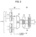
- a concentrator type ATM switching system (referred to as a concentrator, hereinafter), generally designated by 10, according to a first embodiment of the present invention can be used in place of a concentrator 26 in the ATM switching system of Fig. 1.
- the concentrator 10 includes a multiplexing block 30 including a plurality of (m) n-to-1 selectors and a m-to-n multiplexer (MUX) 12, a routing block 13, a concentration buffer block 14, and an output counter 15 consecutively cascaded in the concentrator 10 where m and n are integers and m>n.
- MUX m-to-n multiplexer
- Each of the m selectors 11 receives n input signals each delivered at a rate of V to select one of the n input signals.
- the multiplexer (MUX) 12 receives m input signals each delivered at a rate of nV from m selectors 11 to deliver n multiplexed signal sequences each at a rate of mV.
- the routing block 13 receives n signal sequences from the multiplexer 12 to output the same after assigning the output buffer ports in the concentration buffer block 14 for the m multiplexed signal sequences.
- the concentration buffer block 14 delivers n multiplexed signal sequences each at a rate of V.
- the output counter 15 controls each of m selectors 11.
- the concentration buffer block 14 includes a n ⁇ n banyan network for switching the n multiplexed signal sequences to n output buffer ports based on the assignment signal specified by the routing block 13.
- the concentration buffer block 14 delivers a buffer control signal 16 for informing the present state of storage in the output buffers in the concentration buffer block 14 to the routing block 13.
- input cells supplied to each selector 11 at a rate of V are selected one by one, based on the count output of the counter 15, to be multiplexed into a single signal sequence at a rate of nV.
- Outputs from m selectors 11, which are numbered from #1 to #m, are further multiplexed into n signal sequences at a rate of mV in the m-to-n multiplexer 12 and supplied to the routing block 13.
- the routing block 13 assigns an output port of the concentration buffer block 14 by its number, through which the concentration buffer block 14 delivers the cells, for each effective cell.
- the assigned output port numbers do not overlap one another, because the output port numbers are sequentially assigned to the effective cells in the order of the input ports delivering the effective cells.
- the output port numbers are sequentially assigned basically beginning from the input port #0 without initializing.
- the output port number is set at #0 by an initialization on condition that all the output buffers in the concentration buffer block are empty.
- the present state of storage in the output buffers in the concentration buffer block 14 is informed to the routing block 13 through a buffer control signal 16.
- the routing block 13 may be implemented by a plurality of counters, for example.
- effective cells are delivered by the n ⁇ n banyan network through the output ports specified by the output port numbers assigned by the routing block 13.
- a large-scale ATM switching system such as shown in Fig. 1, is implemented by coupling a plurality of (m) small-scale n ⁇ n ATM switch modules 21 to one another by a coupling module 25 including m concentrators 10 of the present embodiment instead of the m concentrators 26.
- the rout judgement block 24 judges the destination of the input cell and specifies one of the n ⁇ n ATM switch modules 21 based on the destination. All the concentrators 10 judge whether or not the own concentrators are connected to the specified n ⁇ n ATM switch 21, thereby determining whether the data cell supplied thereto is an effective cell or an invalid cell. Thus, one of the concentrators 10 recognizes the data cell as an effective cell for each input cell.
- the information of destination may be supplied to the concentrator 10 as a additional data stored in an excess bit not specified before in the data cell or may be supplied through a separate line. If a plurality of concentrators 10 are allowed to judge the input cell as an effective cell instead, a multi-cast processing operation can be obtained.
- the banyan network 31 includes twelve 2 ⁇ 2 switches 27 as a whole for coupling eight input ports to eight output ports.
- Reference numeral 29 represents an effective cell among the input data cells, and reference numeral 30 represents an invalid cell.
- each effective cell 29 has an output port number specified by the routing block 13.
- the output port number of an effective cell 29 is 6 (110 in a binary notation)
- a corresponding first stage switch 27 selects "0" based on the least significant bit (LSB) of the output port number
- the second stage switch connected to the selected "0" of the first stage switch 27 selects "1” based on the intermediate bit of the first effective cell
- the third stage switch 27 connected to the selected "1" of the second stage switch 27 selects "1” based on the most significant bit (MSB), thereby reaching output port #6 from any of the starting input ports #1 to #6.
- MSB most significant bit
- Fig. 4 showing a step subsequent to the step shown in Fig. 3, next effective cells 29 are supplied through the input ports #0, #2, #6, and #7 at the same time, after the previous cells are stored in the output ports #0 to #4.
- output port numbers following the output port numbers specified by the previous stage is assigned to the effective cells 29, thereby assigning output ports #5, #6, #7 and #0 to the effective cells 29.
- Each effective cells 29 traces the route, shown by a thick line, to be stored in the specified output buffer 28, similarly to the step of Fig. 3.
- a concentrator 10A according to a second embodiment of the present invention is similar to the first embodiment, except that the m-to-n multiplexer 12 is omitted in the present embodiment.
- a concentrator 10B according to a third embodiment of the present invention is similar to the first embodiment except that a plurality of k-to-1 multiplexers 17 each for multiplexing k signal sequences into a single signal sequence are provided instead of the m-to-n multiplexer 12.
- This configuration can be used in the case of m>n.
- m signal lines from the m selectors 11 are divided into m/k groups each including k signal lines ( m/k ⁇ n ), thereby reducing the signal lines input to the banyan network 31 down to equal to n or less.
- the first embodiment and the third embodiment can be selected in the case of m>n depending on the conveniences for data conversion.
- a concentrator 10C according to a fourth embodiment of the present invention is similar to the second embodiment except that a plurality of h-to-1 selectors 18 are provided in the present embodiment instead of n-to-1 selectors 11.
- the number of h-to-1 selectors 18 is determined to be equal to or less than n by selecting a suitable number for h where m ⁇ h.
- the outputs of the multiplexers 18 can be processed by the routing block 13 and the concentration buffer block 14, similarly to the first embodiment or the second embodiment.
- a j ⁇ n switch 14A including a j ⁇ j banyan network 19 and a plurality of (j) 1-to-i demultiplexers (DMUX) 20.
- DMUX 1-to-i demultiplexers
- the j ⁇ n switch 14A can be used instead of the n ⁇ n banyan network 31 in the concentration buffer block 14 in Fig. 2 and Figs. 5 to 7.
- a non-blocking switching operation can be obtained, similarly to the cases shown in Fig. 2 and Figs. 5 to 7, by multiplexing the m ⁇ n input data into j signal sequences, assigning the n output buffers 18 sequentially to the effective cells in the routing block 13, and switching by the j ⁇ n switch 14A shown in Fig. 8.
- the n ⁇ n banyan network 31 has more input/output ports than the j ⁇ n switch 14A so that a processing at a lower transfer rate can be obtained in the band network 31.
- the j ⁇ n switch 14A implemented by the combination of j ⁇ j banyan network 19 and the demultiplexers 20 can achieve a comparatively smaller circuit scale of the concentrator.
- the multiplexers provided in the above embodiments at the stages preceding the routing block 13 in the respective concentrators 10 in Fig. 1 can be combined as a common multiplexer for all the concentrators 10.
- the outputs from the common multiplexer are delivered to the routing blocks 13 and the concentration buffer block 14 in the respective concentrators.
Landscapes
- Engineering & Computer Science (AREA)
- Computer Networks & Wireless Communication (AREA)
- Signal Processing (AREA)
- Data Exchanges In Wide-Area Networks (AREA)
- Use Of Switch Circuits For Exchanges And Methods Of Control Of Multiplex Exchanges (AREA)
Applications Claiming Priority (3)
| Application Number | Priority Date | Filing Date | Title |
|---|---|---|---|
| JP30214797 | 1997-11-04 | ||
| JP30214797A JP3077647B2 (ja) | 1997-11-04 | 1997-11-04 | コンセントレータ型atmスイッチシステム |
| JP302147/97 | 1997-11-04 |
Publications (3)
| Publication Number | Publication Date |
|---|---|
| EP0915593A2 true EP0915593A2 (de) | 1999-05-12 |
| EP0915593A3 EP0915593A3 (de) | 1999-07-28 |
| EP0915593B1 EP0915593B1 (de) | 2006-04-05 |
Family
ID=17905479
Family Applications (1)
| Application Number | Title | Priority Date | Filing Date |
|---|---|---|---|
| EP98120646A Expired - Lifetime EP0915593B1 (de) | 1997-11-04 | 1998-11-03 | ATM-Vermittlungsstelle vom Typ Konzentrator für ein ATM-Vermittlungssystem |
Country Status (5)
| Country | Link |
|---|---|
| US (1) | US6580714B1 (de) |
| EP (1) | EP0915593B1 (de) |
| JP (1) | JP3077647B2 (de) |
| CA (1) | CA2252488C (de) |
| DE (1) | DE69834089T2 (de) |
Cited By (1)
| Publication number | Priority date | Publication date | Assignee | Title |
|---|---|---|---|---|
| EP1187402A3 (de) * | 2000-09-11 | 2004-05-26 | Fujitsu Limited | Vermittlungsstelle, Übertragungsvorrichtung, Übertragungssystem |
Families Citing this family (3)
| Publication number | Priority date | Publication date | Assignee | Title |
|---|---|---|---|---|
| JP3344383B2 (ja) * | 1999-10-04 | 2002-11-11 | 日本電気株式会社 | スケジューラ |
| JP2014045916A (ja) * | 2012-08-31 | 2014-03-17 | Kyokuto Sanki Co Ltd | 内装施工用スポンジ |
| US9998131B1 (en) * | 2016-12-14 | 2018-06-12 | Taiwan Semiconductor Manufacturing Co., Ltd. | Hybrid analog-to-digital converter |
Family Cites Families (12)
| Publication number | Priority date | Publication date | Assignee | Title |
|---|---|---|---|---|
| JP2721195B2 (ja) | 1988-09-19 | 1998-03-04 | 富士通株式会社 | Atm用自己ルーティング集線装置 |
| JP3128654B2 (ja) * | 1990-10-19 | 2001-01-29 | 富士通株式会社 | 監視制御方法、監視制御装置及び交換システム |
| US5256958A (en) | 1991-11-26 | 1993-10-26 | At&T Bell Laboratories | Concentrator-based growable packet switch |
| JP3045865B2 (ja) * | 1992-02-10 | 2000-05-29 | 日本電信電話株式会社 | Atmクロスコネクト装置 |
| JP3354689B2 (ja) | 1994-02-28 | 2002-12-09 | 富士通株式会社 | Atm交換機、交換機及びそのスイッチングパス設定方法 |
| US5412646A (en) * | 1994-05-13 | 1995-05-02 | At&T Corp. | Asynchronous transfer mode switch architecture |
| JP3291122B2 (ja) * | 1994-06-02 | 2002-06-10 | 富士通株式会社 | 自己ルーチング交換機、atm交換機及び交換システム |
| KR960027803A (ko) * | 1994-12-13 | 1996-07-22 | 양승택 | 출력버퍼형 비동기 전송방식(atm) 스위치 |
| JP2854817B2 (ja) * | 1994-12-15 | 1999-02-10 | 韓國電子通信研究院 | グルーピング/トラップ/ルーティング構造を有するatmマルチチャンネルスイッチ |
| US5724352A (en) * | 1995-08-31 | 1998-03-03 | Lucent Technologies Inc. | Terabit per second packet switch having assignable multiple packet loss probabilities |
| JPH10150446A (ja) * | 1996-11-19 | 1998-06-02 | Fujitsu Ltd | Atm交換システム |
| JP2907196B2 (ja) * | 1997-11-06 | 1999-06-21 | 日本電気株式会社 | Atmコンセントレータ |
-
1997
- 1997-11-04 JP JP30214797A patent/JP3077647B2/ja not_active Expired - Fee Related
-
1998
- 1998-11-02 US US09/184,513 patent/US6580714B1/en not_active Expired - Fee Related
- 1998-11-03 EP EP98120646A patent/EP0915593B1/de not_active Expired - Lifetime
- 1998-11-03 CA CA002252488A patent/CA2252488C/en not_active Expired - Fee Related
- 1998-11-03 DE DE69834089T patent/DE69834089T2/de not_active Expired - Lifetime
Cited By (2)
| Publication number | Priority date | Publication date | Assignee | Title |
|---|---|---|---|---|
| EP1187402A3 (de) * | 2000-09-11 | 2004-05-26 | Fujitsu Limited | Vermittlungsstelle, Übertragungsvorrichtung, Übertragungssystem |
| US6947413B2 (en) | 2000-09-11 | 2005-09-20 | Fujitsu Limited | Switching apparatus, communication apparatus, and communication system |
Also Published As
| Publication number | Publication date |
|---|---|
| US6580714B1 (en) | 2003-06-17 |
| JPH11145961A (ja) | 1999-05-28 |
| EP0915593A3 (de) | 1999-07-28 |
| EP0915593B1 (de) | 2006-04-05 |
| DE69834089T2 (de) | 2006-08-24 |
| JP3077647B2 (ja) | 2000-08-14 |
| CA2252488A1 (en) | 1999-05-04 |
| CA2252488C (en) | 2004-08-17 |
| DE69834089D1 (de) | 2006-05-18 |
Similar Documents
| Publication | Publication Date | Title |
|---|---|---|
| US6289011B1 (en) | 2n×n multiplexing switch | |
| EP0256701B1 (de) | Koppelpunktschaltung für Datenpaketraumvermittlung | |
| EP0300061B1 (de) | Selbstsuchendes vermittlungssystem | |
| US5361255A (en) | Method and apparatus for a high speed asynchronous transfer mode switch | |
| EP0785699B1 (de) | Mehrfachsende-Leitweglenkung in mehrstufigen Netzen | |
| EP0868054B1 (de) | Selbstarbitrierender Kreuzschienenschalter | |
| AU693084B2 (en) | Controlled access ATM switch | |
| US6188690B1 (en) | Method and apparatus for high speed, scalable communication system | |
| JP2907886B2 (ja) | スイッチングシステム | |
| EP0590865B1 (de) | Mehrstufige erweiterbare optische Paketverteilanordnung mit Überbrückungsschalter | |
| KR19980064825A (ko) | 에이.티.엠 스위치의 분산 버퍼링 시스템 | |
| US5285444A (en) | Multi-stage link switch | |
| US5268896A (en) | Communication switching element | |
| EP0542233A2 (de) | Einrichtung und Verfahren zur Zellenvermittlung | |
| RU2129751C1 (ru) | Коммутационная система для выполнения асинхронного режима передачи и способ коммутации ячеек в ней | |
| KR100246627B1 (ko) | 트래픽 흐름제어 및 감시기능을 갖는 멀티채널 패킷 스위칭 장치 | |
| EP1041772B1 (de) | Paketvermittlungseinrichtung zur Paketübertragung ohne Verzögerung | |
| EP0915593B1 (de) | ATM-Vermittlungsstelle vom Typ Konzentrator für ein ATM-Vermittlungssystem | |
| US20060104281A1 (en) | Packet routing | |
| EP0417083B1 (de) | Kommunikationsvermittlungselement | |
| JPH077520A (ja) | ローカルネットワークおよびブリッジ素子 | |
| JP2751832B2 (ja) | Atm網および網構成装置 | |
| JPH0819012A (ja) | 波長多重型光パケットスイッチモジュールおよび光パケットスイッチ回路網 | |
| KR0173212B1 (ko) | 우회링크를 이용한 출력버퍼형 비동기전달모드 스위칭장치 | |
| KR960007674B1 (ko) | 비대칭 제한적 공유메모리 비동기 전달모드(ATM:Asynchronous Transfef Mode) 스위치 장치 |
Legal Events
| Date | Code | Title | Description |
|---|---|---|---|
| PUAI | Public reference made under article 153(3) epc to a published international application that has entered the european phase |
Free format text: ORIGINAL CODE: 0009012 |
|
| AK | Designated contracting states |
Kind code of ref document: A2 Designated state(s): DE FR |
|
| AX | Request for extension of the european patent |
Free format text: AL;LT;LV;MK;RO;SI |
|
| PUAL | Search report despatched |
Free format text: ORIGINAL CODE: 0009013 |
|
| AK | Designated contracting states |
Kind code of ref document: A3 Designated state(s): AT BE CH CY DE DK ES FI FR GB GR IE IT LI LU MC NL PT SE |
|
| AX | Request for extension of the european patent |
Free format text: AL;LT;LV;MK;RO;SI |
|
| 17P | Request for examination filed |
Effective date: 19990623 |
|
| AKX | Designation fees paid |
Free format text: DE FR |
|
| 17Q | First examination report despatched |
Effective date: 20041014 |
|
| RAP1 | Party data changed (applicant data changed or rights of an application transferred) |
Owner name: JUNIPER NETWORKS, INC. |
|
| GRAP | Despatch of communication of intention to grant a patent |
Free format text: ORIGINAL CODE: EPIDOSNIGR1 |
|
| GRAS | Grant fee paid |
Free format text: ORIGINAL CODE: EPIDOSNIGR3 |
|
| GRAA | (expected) grant |
Free format text: ORIGINAL CODE: 0009210 |
|
| AK | Designated contracting states |
Kind code of ref document: B1 Designated state(s): DE FR |
|
| REF | Corresponds to: |
Ref document number: 69834089 Country of ref document: DE Date of ref document: 20060518 Kind code of ref document: P |
|
| ET | Fr: translation filed | ||
| PLBE | No opposition filed within time limit |
Free format text: ORIGINAL CODE: 0009261 |
|
| STAA | Information on the status of an ep patent application or granted ep patent |
Free format text: STATUS: NO OPPOSITION FILED WITHIN TIME LIMIT |
|
| 26N | No opposition filed |
Effective date: 20070108 |
|
| PGFP | Annual fee paid to national office [announced via postgrant information from national office to epo] |
Ref country code: DE Payment date: 20131127 Year of fee payment: 16 Ref country code: FR Payment date: 20131118 Year of fee payment: 16 |
|
| REG | Reference to a national code |
Ref country code: DE Ref legal event code: R119 Ref document number: 69834089 Country of ref document: DE |
|
| REG | Reference to a national code |
Ref country code: FR Ref legal event code: ST Effective date: 20150731 |
|
| PG25 | Lapsed in a contracting state [announced via postgrant information from national office to epo] |
Ref country code: DE Free format text: LAPSE BECAUSE OF NON-PAYMENT OF DUE FEES Effective date: 20150602 |
|
| PG25 | Lapsed in a contracting state [announced via postgrant information from national office to epo] |
Ref country code: FR Free format text: LAPSE BECAUSE OF NON-PAYMENT OF DUE FEES Effective date: 20141201 |