EP0917208A1 - Polymer-nanocrystal photo device and method for making the same - Google Patents
Polymer-nanocrystal photo device and method for making the same Download PDFInfo
- Publication number
- EP0917208A1 EP0917208A1 EP97203499A EP97203499A EP0917208A1 EP 0917208 A1 EP0917208 A1 EP 0917208A1 EP 97203499 A EP97203499 A EP 97203499A EP 97203499 A EP97203499 A EP 97203499A EP 0917208 A1 EP0917208 A1 EP 0917208A1
- Authority
- EP
- European Patent Office
- Prior art keywords
- photo device
- tio
- sized particles
- conducting polymer
- ppv
- Prior art date
- Legal status (The legal status is an assumption and is not a legal conclusion. Google has not performed a legal analysis and makes no representation as to the accuracy of the status listed.)
- Withdrawn
Links
Images
Classifications
-
- H—ELECTRICITY
- H10—SEMICONDUCTOR DEVICES; ELECTRIC SOLID-STATE DEVICES NOT OTHERWISE PROVIDED FOR
- H10K—ORGANIC ELECTRIC SOLID-STATE DEVICES
- H10K30/00—Organic devices sensitive to infrared radiation, light, electromagnetic radiation of shorter wavelength or corpuscular radiation
- H10K30/10—Organic devices sensitive to infrared radiation, light, electromagnetic radiation of shorter wavelength or corpuscular radiation comprising heterojunctions between organic semiconductors and inorganic semiconductors
- H10K30/15—Sensitised wide-bandgap semiconductor devices, e.g. dye-sensitised TiO2
- H10K30/151—Sensitised wide-bandgap semiconductor devices, e.g. dye-sensitised TiO2 the wide bandgap semiconductor comprising titanium oxide, e.g. TiO2
-
- B—PERFORMING OPERATIONS; TRANSPORTING
- B82—NANOTECHNOLOGY
- B82Y—SPECIFIC USES OR APPLICATIONS OF NANOSTRUCTURES; MEASUREMENT OR ANALYSIS OF NANOSTRUCTURES; MANUFACTURE OR TREATMENT OF NANOSTRUCTURES
- B82Y20/00—Nanooptics, e.g. quantum optics or photonic crystals
-
- B—PERFORMING OPERATIONS; TRANSPORTING
- B82—NANOTECHNOLOGY
- B82Y—SPECIFIC USES OR APPLICATIONS OF NANOSTRUCTURES; MEASUREMENT OR ANALYSIS OF NANOSTRUCTURES; MANUFACTURE OR TREATMENT OF NANOSTRUCTURES
- B82Y30/00—Nanotechnology for materials or surface science, e.g. nanocomposites
-
- H—ELECTRICITY
- H10—SEMICONDUCTOR DEVICES; ELECTRIC SOLID-STATE DEVICES NOT OTHERWISE PROVIDED FOR
- H10K—ORGANIC ELECTRIC SOLID-STATE DEVICES
- H10K30/00—Organic devices sensitive to infrared radiation, light, electromagnetic radiation of shorter wavelength or corpuscular radiation
- H10K30/30—Organic devices sensitive to infrared radiation, light, electromagnetic radiation of shorter wavelength or corpuscular radiation comprising bulk heterojunctions, e.g. interpenetrating networks of donor and acceptor material domains
- H10K30/35—Organic devices sensitive to infrared radiation, light, electromagnetic radiation of shorter wavelength or corpuscular radiation comprising bulk heterojunctions, e.g. interpenetrating networks of donor and acceptor material domains comprising inorganic nanostructures, e.g. CdSe nanoparticles
-
- H—ELECTRICITY
- H10—SEMICONDUCTOR DEVICES; ELECTRIC SOLID-STATE DEVICES NOT OTHERWISE PROVIDED FOR
- H10K—ORGANIC ELECTRIC SOLID-STATE DEVICES
- H10K50/00—Organic light-emitting devices
- H10K50/10—OLEDs or polymer light-emitting diodes [PLED]
- H10K50/11—OLEDs or polymer light-emitting diodes [PLED] characterised by the electroluminescent [EL] layers
-
- H—ELECTRICITY
- H10—SEMICONDUCTOR DEVICES; ELECTRIC SOLID-STATE DEVICES NOT OTHERWISE PROVIDED FOR
- H10K—ORGANIC ELECTRIC SOLID-STATE DEVICES
- H10K2102/00—Constructional details relating to the organic devices covered by this subclass
- H10K2102/301—Details of OLEDs
- H10K2102/331—Nanoparticles used in non-emissive layers, e.g. in packaging layer
-
- H—ELECTRICITY
- H10—SEMICONDUCTOR DEVICES; ELECTRIC SOLID-STATE DEVICES NOT OTHERWISE PROVIDED FOR
- H10K—ORGANIC ELECTRIC SOLID-STATE DEVICES
- H10K30/00—Organic devices sensitive to infrared radiation, light, electromagnetic radiation of shorter wavelength or corpuscular radiation
- H10K30/50—Photovoltaic [PV] devices
-
- H—ELECTRICITY
- H10—SEMICONDUCTOR DEVICES; ELECTRIC SOLID-STATE DEVICES NOT OTHERWISE PROVIDED FOR
- H10K—ORGANIC ELECTRIC SOLID-STATE DEVICES
- H10K85/00—Organic materials used in the body or electrodes of devices covered by this subclass
- H10K85/10—Organic polymers or oligomers
- H10K85/111—Organic polymers or oligomers comprising aromatic, heteroaromatic, or aryl chains, e.g. polyaniline, polyphenylene or polyphenylene vinylene
- H10K85/114—Poly-phenylenevinylene; Derivatives thereof
-
- Y—GENERAL TAGGING OF NEW TECHNOLOGICAL DEVELOPMENTS; GENERAL TAGGING OF CROSS-SECTIONAL TECHNOLOGIES SPANNING OVER SEVERAL SECTIONS OF THE IPC; TECHNICAL SUBJECTS COVERED BY FORMER USPC CROSS-REFERENCE ART COLLECTIONS [XRACs] AND DIGESTS
- Y02—TECHNOLOGIES OR APPLICATIONS FOR MITIGATION OR ADAPTATION AGAINST CLIMATE CHANGE
- Y02E—REDUCTION OF GREENHOUSE GAS [GHG] EMISSIONS, RELATED TO ENERGY GENERATION, TRANSMISSION OR DISTRIBUTION
- Y02E10/00—Energy generation through renewable energy sources
- Y02E10/50—Photovoltaic [PV] energy
- Y02E10/549—Organic PV cells
-
- Y—GENERAL TAGGING OF NEW TECHNOLOGICAL DEVELOPMENTS; GENERAL TAGGING OF CROSS-SECTIONAL TECHNOLOGIES SPANNING OVER SEVERAL SECTIONS OF THE IPC; TECHNICAL SUBJECTS COVERED BY FORMER USPC CROSS-REFERENCE ART COLLECTIONS [XRACs] AND DIGESTS
- Y02—TECHNOLOGIES OR APPLICATIONS FOR MITIGATION OR ADAPTATION AGAINST CLIMATE CHANGE
- Y02P—CLIMATE CHANGE MITIGATION TECHNOLOGIES IN THE PRODUCTION OR PROCESSING OF GOODS
- Y02P70/00—Climate change mitigation technologies in the production process for final industrial or consumer products
- Y02P70/50—Manufacturing or production processes characterised by the final manufactured product
Definitions
- This invention intends to offer a solution to the problem of creating an interpenetrating solid-state conducting material in a nanoporous network, for the purpose of creating stable, all-solid state photovoltaic cells.
- the instability problems associated with liquid-based electrolytes in nanoporous networks (1) can be eliminated.
- Prior methods have been published on the insertion of a polymer electrolyte into a preformed nanocrystalline TiO 2 (titanium dioxide) network (2) but this methods have the disadvantage of being based on an ionic conductor thus limiting the device performance, rather than on an electronic conductor such as the one we describe here.
- Another prior method using conducting polymers replaces the inorganic nanocrystalline network with C 60 and derivatives which act as electron-acceptors (3).
- the present invention offers the stability, electron tranporting properties, and low cost of a TiO 2 interconnected network in combination with the hole-transporting, light-absorbing, stable properties of PPV (poly-paraphenylenevinylene).
- a further aspect of this invention is the ease of manufacturing, namely in a single thermal treatment of the inorganic and organic materials together.
- An example of this method according to this invention uses a conducting polymer, p-PPV (precursor PPV) and a nanocrystalline material, TiO 2 .
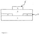
- a schematic cross-section of the cell is show, in Fig. 1.
- the polymer p-PPV was made by chemical synthesis (4).
- TiO 2 nanocrystals were obtained from Degussa AG corporation, Germany.
- An approximately 0.7% methanol solution of the p-PPV was combined with a colloid of TiO 2 made according to reference 5 to give a mixture of approximately 1:1 p-PPV and TiO 2 ,by weight.
- This mixture was spin-coated on a glass substrate 1 with a transparent conducting coating 2, in this example SnO2:F, to give a thin film 3.
- the film was heated to 320 °C for ten hours in vacuum and an aluminum contact 4 evaporated in such a way that there is no overlap with the transparent (with methods commonly known in the field), conducting coating on the glass on top of the film to complete
- the main novelty and crucial distinction of this method over other methods is the thermal treatment step, which is necessary for both conversion of the p-PPV to its final conducting form, PPV; and, to produce electrical contact between the TiO 2 particles to produce electron-carrying paths through the film.
- Our method is the first one to make operational photovoltaic cells of a conducting polymer, such as PPV, and a sintered electrically interconnected network of nanocrystalline particles, such as TiO 2 .
- PPV has been shown to be a good hole-conducting material (4) and TiO 2 an excellent electron transporter (1), so their combination together, prepared in a single thermal treatment step, also represents a significant advance.
- the method is general for a range of temperatures, other polymers, or nanocrystals.
Landscapes
- Chemical & Material Sciences (AREA)
- Engineering & Computer Science (AREA)
- Physics & Mathematics (AREA)
- Nanotechnology (AREA)
- Crystallography & Structural Chemistry (AREA)
- Optics & Photonics (AREA)
- Inorganic Chemistry (AREA)
- Electromagnetism (AREA)
- Life Sciences & Earth Sciences (AREA)
- Biophysics (AREA)
- Composite Materials (AREA)
- Condensed Matter Physics & Semiconductors (AREA)
- General Physics & Mathematics (AREA)
- Materials Engineering (AREA)
- Hybrid Cells (AREA)
- Photovoltaic Devices (AREA)
- Inorganic Compounds Of Heavy Metals (AREA)
Abstract
Especially for reducing costs for photovoltaic cells, research is
done all around the world for finding a solid state composition of
creating an interpenetrating solid-state conducting material in a
nanoporous network. Such device could also be used for LED (light
emitting diodes), photo sensors, optical switches and even optical
networks.
This invention relates to a photo device comprising a layer
of nanometer sized particles and a conducting polymer in solid state,
wherein
the nanometer sized particles are chosen from the group of TiO2, ZnO, CdSe, CdS, ZrO2, SnO2 and
wherein the conducting polymer comprises PPV (polyparaphenylenevinylene) or a derivative thereof.
the nanometer sized particles are chosen from the group of TiO2, ZnO, CdSe, CdS, ZrO2, SnO2 and
wherein the conducting polymer comprises PPV (polyparaphenylenevinylene) or a derivative thereof.
Description
- Especially for reducing costs for photovoltaic cells, research is done all around the world for finding a solid state composition of creating a interpenetrating solid-state conducting material in a nanoporous network. Such device could also be used for LED (light emitting diodes), photo sensors, optical switches and even optical networks.
- This invention intends to offer a solution to the problem of creating an interpenetrating solid-state conducting material in a nanoporous network, for the purpose of creating stable, all-solid state photovoltaic cells. Thus, the instability problems associated with liquid-based electrolytes in nanoporous networks (1) can be eliminated. Prior methods have been published on the insertion of a polymer electrolyte into a preformed nanocrystalline TiO2 (titanium dioxide) network (2) but this methods have the disadvantage of being based on an ionic conductor thus limiting the device performance, rather than on an electronic conductor such as the one we describe here. Another prior method using conducting polymers (PPV and derivatives) replaces the inorganic nanocrystalline network with C60 and derivatives which act as electron-acceptors (3). However, in this method, the electron transport is restricted. Further, C60 is not a material which can be produced abundantly, and is thus expensive; it is also much less stable than inorganic materials. The present invention offers the stability, electron tranporting properties, and low cost of a TiO2 interconnected network in combination with the hole-transporting, light-absorbing, stable properties of PPV (poly-paraphenylenevinylene). A further aspect of this invention is the ease of manufacturing, namely in a single thermal treatment of the inorganic and organic materials together.
- An example of this method according to this invention uses a conducting polymer, p-PPV (precursor PPV) and a nanocrystalline material, TiO2. A schematic cross-section of the cell is show, in Fig. 1. The polymer p-PPV was made by chemical synthesis (4). TiO2 nanocrystals were obtained from Degussa AG corporation, Germany. An approximately 0.7% methanol solution of the p-PPV was combined with a colloid of TiO2 made according to
reference 5 to give a mixture of approximately 1:1 p-PPV and TiO2,by weight. This mixture was spin-coated on a glass substrate 1 with a transparent conducting coating 2, in this example SnO2:F, to give athin film 3. The film was heated to 320 °C for ten hours in vacuum and analuminum contact 4 evaporated in such a way that there is no overlap with the transparent (with methods commonly known in the field), conducting coating on the glass on top of the film to complete the cell. - Current-voltage (IV) curves of the cells in the dark and in white light were measured at
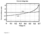
terminals 5 and 6 (Fig. 1) and a plot of this data is shown in Fig. 2 which demonstrates that the cells produce electric power under illumination. - The main novelty and crucial distinction of this method over other methods is the thermal treatment step, which is necessary for both conversion of the p-PPV to its final conducting form, PPV; and, to produce electrical contact between the TiO2 particles to produce electron-carrying paths through the film. Our method is the first one to make operational photovoltaic cells of a conducting polymer, such as PPV, and a sintered electrically interconnected network of nanocrystalline particles, such as TiO2. PPV has been shown to be a good hole-conducting material (4) and TiO2 an excellent electron transporter (1), so their combination together, prepared in a single thermal treatment step, also represents a significant advance.
- The method is general for a range of temperatures, other polymers, or nanocrystals.
Claims (6)
- A photo device comprising a layer of nanometer sized particles and a conducting polymer in solid state.
- A photo device according to claim 1, wherein the nanometer sized particles are chosen from the group of TiO2, ZnO, CdSe, CdS, ZrO2, SnO2.
- A photo device according to claim 1 or 2, wherein the conducting polymer comprises PPV (polyparaphenylenevinylene) or a derivative thereof.
- A photo device according to claim 1, 2 or 3, wherein the layer is a thin film of a photovoltaic cell.
- A method for producing a photo device, according to claim 1, wherein the layer is heated to a predetermined temperature during a predetermined time.
- A method according to claim 5, wherein the heating takes place at substantial underpressure or vacuum.
Priority Applications (5)
| Application Number | Priority Date | Filing Date | Title |
|---|---|---|---|
| EP97203499A EP0917208A1 (en) | 1997-11-11 | 1997-11-11 | Polymer-nanocrystal photo device and method for making the same |
| US09/554,178 US6512172B1 (en) | 1997-11-11 | 1998-11-11 | Polymer-nanocrystal photo device and method for making the same |
| EP98958244A EP1029366A1 (en) | 1997-11-11 | 1998-11-11 | Polymer-nanocrystal photo device and method for making the same |
| PCT/EP1998/007328 WO1999025028A1 (en) | 1997-11-11 | 1998-11-11 | Polymer-nanocrystal photo device and method for making the same |
| AU14355/99A AU1435599A (en) | 1997-11-11 | 1998-11-11 | Polymer-nanocrystal photo device and method for making the same |
Applications Claiming Priority (1)
| Application Number | Priority Date | Filing Date | Title |
|---|---|---|---|
| EP97203499A EP0917208A1 (en) | 1997-11-11 | 1997-11-11 | Polymer-nanocrystal photo device and method for making the same |
Publications (1)
| Publication Number | Publication Date |
|---|---|
| EP0917208A1 true EP0917208A1 (en) | 1999-05-19 |
Family
ID=8228916
Family Applications (2)
| Application Number | Title | Priority Date | Filing Date |
|---|---|---|---|
| EP97203499A Withdrawn EP0917208A1 (en) | 1997-11-11 | 1997-11-11 | Polymer-nanocrystal photo device and method for making the same |
| EP98958244A Withdrawn EP1029366A1 (en) | 1997-11-11 | 1998-11-11 | Polymer-nanocrystal photo device and method for making the same |
Family Applications After (1)
| Application Number | Title | Priority Date | Filing Date |
|---|---|---|---|
| EP98958244A Withdrawn EP1029366A1 (en) | 1997-11-11 | 1998-11-11 | Polymer-nanocrystal photo device and method for making the same |
Country Status (4)
| Country | Link |
|---|---|
| US (1) | US6512172B1 (en) |
| EP (2) | EP0917208A1 (en) |
| AU (1) | AU1435599A (en) |
| WO (1) | WO1999025028A1 (en) |
Cited By (9)
| Publication number | Priority date | Publication date | Assignee | Title |
|---|---|---|---|---|
| GB2389230A (en) * | 2002-05-28 | 2003-12-03 | Univ Nat Taiwan | Nanoparticle light emitting device (LED) |
| FR2862429A1 (en) * | 2003-11-17 | 2005-05-20 | Commissariat Energie Atomique | Producing semiconductor material useful in photovoltaic cells comprises grafting a porous oxide ceramic substrate with a compound that can be polymerized with a precursor of an electrically conductive polymer |
| US7196333B1 (en) * | 1999-09-23 | 2007-03-27 | Commissariat A L'energie Atomique | Radiation detector using a composite material and method for making same |
| CN100366665C (en) * | 2005-12-29 | 2008-02-06 | 复旦大学 | Method for preparing inorganic semiconductor/conductive polymer composite film by photocatalytic polymerization |
| WO2011052511A1 (en) * | 2009-10-29 | 2011-05-05 | 住友化学株式会社 | Organic photoelectric conversion element |
| WO2011015993A3 (en) * | 2009-08-07 | 2011-08-04 | Solargenius S.R.L. | Multilayer photovoltaic composition and method of application |
| CN103597286A (en) * | 2011-06-06 | 2014-02-19 | 肖特公开股份有限公司 | Display device |
| CN103915568A (en) * | 2013-01-06 | 2014-07-09 | 吉林师范大学 | CdS organic electroluminescence device |
| US9196847B2 (en) | 2005-12-23 | 2015-11-24 | Commissariat A L'energie Atomique | Sensitizing complexes, process for the preparation thereof, semiconductive inorganic/organic hybrid material comprising them, and photovoltaic cell comprising said material |
Families Citing this family (34)
| Publication number | Priority date | Publication date | Assignee | Title |
|---|---|---|---|---|
| US6239355B1 (en) * | 1998-10-09 | 2001-05-29 | The Trustees Of Columbia University In The City Of New York | Solid-state photoelectric device |
| US20020110180A1 (en) * | 2001-02-09 | 2002-08-15 | Barney Alfred A. | Temperature-sensing composition |
| CA2460796C (en) * | 2001-09-17 | 2011-02-01 | Vikram C. Sundar | Semiconductor nanocrystal composite |
| US7777303B2 (en) | 2002-03-19 | 2010-08-17 | The Regents Of The University Of California | Semiconductor-nanocrystal/conjugated polymer thin films |
| EP1485955B1 (en) * | 2002-03-19 | 2019-02-13 | The Regents of The University of California | Photovoltaic devices comprising semiconductor-nanocrystal - conjugated polymer thin films |
| KR100495625B1 (en) * | 2002-04-23 | 2005-06-16 | 대주전자재료 주식회사 | Conjugated polymer-inorganic particulate composite composition for luminescent layer of organic electroluminescence device |
| US20040126582A1 (en) * | 2002-08-23 | 2004-07-01 | Nano-Proprietary, Inc. | Silicon nanoparticles embedded in polymer matrix |
| JP2005538573A (en) * | 2002-09-05 | 2005-12-15 | ナノシス・インク. | Compositions based on nanostructures and nanocomposites |
| US6949206B2 (en) * | 2002-09-05 | 2005-09-27 | Nanosys, Inc. | Organic species that facilitate charge transfer to or from nanostructures |
| US7572393B2 (en) * | 2002-09-05 | 2009-08-11 | Nanosys Inc. | Organic species that facilitate charge transfer to or from nanostructures |
| US7534488B2 (en) | 2003-09-10 | 2009-05-19 | The Regents Of The University Of California | Graded core/shell semiconductor nanorods and nanorod barcodes |
| EP1584114A1 (en) * | 2003-01-17 | 2005-10-12 | Diode Solutions, Inc. | Display employing organic material |
| CN1309097C (en) * | 2004-03-24 | 2007-04-04 | 武汉大学 | Method of increasing photoelectricity convesion efficiency of TiO2 photecell |
| DE102004030628A1 (en) * | 2004-06-24 | 2006-01-19 | Konarka Technologies, Inc., Lowell | Organic electronic element with electrically conductive semitransparent layer |
| TWI271876B (en) * | 2005-05-27 | 2007-01-21 | Univ Nat Taiwan | Block copolymer containing nano-particles, electron transporting material and photoelectric device employing the same |
| US8835941B2 (en) * | 2006-02-09 | 2014-09-16 | Qd Vision, Inc. | Displays including semiconductor nanocrystals and methods of making same |
| KR100754396B1 (en) * | 2006-02-16 | 2007-08-31 | 삼성전자주식회사 | Quantum dot light emitting device and manufacturing method thereof |
| WO2007143197A2 (en) * | 2006-06-02 | 2007-12-13 | Qd Vision, Inc. | Light-emitting devices and displays with improved performance |
| WO2007112088A2 (en) * | 2006-03-24 | 2007-10-04 | Qd Vision, Inc. | Hyperspectral imaging device |
| KR101061530B1 (en) * | 2006-04-04 | 2011-09-01 | 6엔 실리콘 아이엔씨. | Purification method of silicon |
| US20070254996A1 (en) * | 2006-04-28 | 2007-11-01 | Krzysztof Nauka | Nanocrystal-polymer composite materials and methods of attaching nanocrystals to polymer molecules |
| WO2008085210A2 (en) * | 2006-09-12 | 2008-07-17 | Qd Vision, Inc. | Electroluminescent display useful for displaying a predetermined pattern |
| US7898042B2 (en) | 2006-11-07 | 2011-03-01 | Cbrite Inc. | Two-terminal switching devices and their methods of fabrication |
| US8222077B2 (en) * | 2006-11-07 | 2012-07-17 | Cbrite Inc. | Metal-insulator-metal (MIM) devices and their methods of fabrication |
| US9741901B2 (en) | 2006-11-07 | 2017-08-22 | Cbrite Inc. | Two-terminal electronic devices and their methods of fabrication |
| WO2008063657A2 (en) * | 2006-11-21 | 2008-05-29 | Qd Vision, Inc. | Light emitting devices and displays with improved performance |
| US9525148B2 (en) | 2008-04-03 | 2016-12-20 | Qd Vision, Inc. | Device including quantum dots |
| CN102047098B (en) | 2008-04-03 | 2016-05-04 | Qd视光有限公司 | Light emitting device including quantum dots |
| EP2403006A4 (en) * | 2009-02-27 | 2014-04-02 | Nat Inst For Materials Science | HETERONJUNCTION SEM SEMICONDUCTOR AND METHOD FOR PRODUCING THE SAME |
| WO2011133228A2 (en) | 2010-04-23 | 2011-10-27 | Pixelligent Technologies, Llc | Synthesis, capping and dispersion of nanocrystals |
| EP3190083B1 (en) | 2010-10-27 | 2020-08-26 | Pixelligent Technologies, LLC | Synthesis, capping and dispersion of nanocrystals |
| US9359689B2 (en) | 2011-10-26 | 2016-06-07 | Pixelligent Technologies, Llc | Synthesis, capping and dispersion of nanocrystals |
| CN108435260A (en) * | 2018-03-26 | 2018-08-24 | 江苏奥净嘉环保科技有限公司 | A kind of preparation method of nano-titanium dioxide cadmium sulfide composite photo-catalyst |
| CN115483352A (en) * | 2022-09-14 | 2022-12-16 | 暨南大学 | Vacuum vapor deposition preparation method of a large-area high-quality perovskite film and photovoltaic devices prepared using the perovskite film |
Family Cites Families (2)
| Publication number | Priority date | Publication date | Assignee | Title |
|---|---|---|---|---|
| JP2002502129A (en) * | 1998-02-02 | 2002-01-22 | ユニアックス コーポレイション | Organic diodes with switchable photoelectric sensitivity |
| US6239355B1 (en) * | 1998-10-09 | 2001-05-29 | The Trustees Of Columbia University In The City Of New York | Solid-state photoelectric device |
-
1997
- 1997-11-11 EP EP97203499A patent/EP0917208A1/en not_active Withdrawn
-
1998
- 1998-11-11 EP EP98958244A patent/EP1029366A1/en not_active Withdrawn
- 1998-11-11 AU AU14355/99A patent/AU1435599A/en not_active Abandoned
- 1998-11-11 WO PCT/EP1998/007328 patent/WO1999025028A1/en not_active Ceased
- 1998-11-11 US US09/554,178 patent/US6512172B1/en not_active Expired - Fee Related
Non-Patent Citations (4)
| Title |
|---|
| KUCZKOWSKI A: "THE PROSPECTS FOR POLYESTER POLYMER-CDS POWER COMPOSITES IN PHOTOELECTRONIC DEVICE APPLICATIONS", JOURNAL OF PHYSICS D. APPLIED PHYSICS, vol. 22, no. 11, 14 November 1989 (1989-11-14), BRISTOL, GB, pages 1731 - 1735, XP000072966 * |
| N.C. GREENHAM ET AL.: "Charge separation and transport in conjugated polymer/cadmium selenide nanocrystal composites studied by photoluminescence quenching and photoconductivity", SYNTHETIC METALS, vol. 84, no. 1-3, 1 January 1997 (1997-01-01), AMSTERDAM, NL, pages 545 - 546, XP002060965 * |
| N.C. GREENHAM ET AL.: "Charge separation and transport in conjugated-polymer/semiconductor-nanocrystal composites studied by photoluminescence quenching and photoconductivity", PHYSICAL REVIEW, B. CONDENSED MATTER., vol. 54, no. 24, 15 December 1996 (1996-12-15), NEW YORK US, pages 17628 - 17637, XP002060964 * |
| S.A. CARTER ET AL.: "Enhanced luminance in polymer composite light emitting devices", APPLIED PHYSICS LETTERS., vol. 71, no. 9, 1 September 1997 (1997-09-01), NEW YORK US, pages 1145 - 1147, XP000720223 * |
Cited By (13)
| Publication number | Priority date | Publication date | Assignee | Title |
|---|---|---|---|---|
| US7196333B1 (en) * | 1999-09-23 | 2007-03-27 | Commissariat A L'energie Atomique | Radiation detector using a composite material and method for making same |
| GB2389230A (en) * | 2002-05-28 | 2003-12-03 | Univ Nat Taiwan | Nanoparticle light emitting device (LED) |
| FR2862429A1 (en) * | 2003-11-17 | 2005-05-20 | Commissariat Energie Atomique | Producing semiconductor material useful in photovoltaic cells comprises grafting a porous oxide ceramic substrate with a compound that can be polymerized with a precursor of an electrically conductive polymer |
| WO2005050752A1 (en) * | 2003-11-17 | 2005-06-02 | Commissariat A L'energie Atomique | Inorganic/organic semiconductor p-n hybrid material, production method thereof and photovoltaic cell comprising same |
| US9196847B2 (en) | 2005-12-23 | 2015-11-24 | Commissariat A L'energie Atomique | Sensitizing complexes, process for the preparation thereof, semiconductive inorganic/organic hybrid material comprising them, and photovoltaic cell comprising said material |
| CN100366665C (en) * | 2005-12-29 | 2008-02-06 | 复旦大学 | Method for preparing inorganic semiconductor/conductive polymer composite film by photocatalytic polymerization |
| WO2011015993A3 (en) * | 2009-08-07 | 2011-08-04 | Solargenius S.R.L. | Multilayer photovoltaic composition and method of application |
| JP2011119697A (en) * | 2009-10-29 | 2011-06-16 | Sumitomo Chemical Co Ltd | Organic photoelectric conversion element |
| WO2011052511A1 (en) * | 2009-10-29 | 2011-05-05 | 住友化学株式会社 | Organic photoelectric conversion element |
| CN103597286A (en) * | 2011-06-06 | 2014-02-19 | 肖特公开股份有限公司 | Display device |
| CN103597286B (en) * | 2011-06-06 | 2016-07-20 | 肖特公开股份有限公司 | Display device |
| CN103915568A (en) * | 2013-01-06 | 2014-07-09 | 吉林师范大学 | CdS organic electroluminescence device |
| CN103915568B (en) * | 2013-01-06 | 2016-07-20 | 吉林师范大学 | A kind of CdS organic electroluminescence device |
Also Published As
| Publication number | Publication date |
|---|---|
| WO1999025028A1 (en) | 1999-05-20 |
| EP1029366A1 (en) | 2000-08-23 |
| US6512172B1 (en) | 2003-01-28 |
| AU1435599A (en) | 1999-05-31 |
Similar Documents
| Publication | Publication Date | Title |
|---|---|---|
| EP0917208A1 (en) | Polymer-nanocrystal photo device and method for making the same | |
| Zhang et al. | High-efficiency (> 20%) planar carbon-based perovskite solar cells through device configuration engineering | |
| Zhang et al. | Polymer photovoltaic cells with conducting polymer anodes | |
| O'Regan et al. | Electrodeposited nanocomposite n–p heterojunctions for solid‐state dye‐sensitized photovoltaics | |
| Khandelwal et al. | Semitransparent organic solar cells: from molecular design to structure–performance relationships | |
| Dou et al. | Perovskite‐based indoor photovoltaics and their competitors | |
| Suthar et al. | Indoor organic solar cells for low-power IoT devices: recent progress, challenges, and applications | |
| Chen et al. | Multilayer Cascade Charge Transport Layer for High‐Performance Inverted Mesoscopic All‐Inorganic and Hybrid Wide‐Bandgap Perovskite Solar Cells | |
| Lee et al. | Thin metal top electrode and interface engineering for efficient and air-stable semitransparent perovskite solar cells | |
| Zhao et al. | Metallic tin substitution of organic lead perovskite films for efficient solar cells | |
| Kim et al. | Nip-type perovskite solar cells employing n-type graphene transparent conductive electrodes | |
| Cho et al. | Efficient ITO-free semitransparent perovskite solar cells with metal transparent electrodes | |
| EP2073226A2 (en) | Dye-sensitized solar cell and method of manufacturing the same | |
| CN102142521A (en) | Organic solar battery and preparation method thereof | |
| CA3183150A1 (en) | Semi-transparent perovskite-based photovoltaic cells and process for preparing them | |
| Jiang et al. | Efficient perovskite indoor photovoltaics with open‐circuit voltage of 1.15 V via collaborative optimization of CsPbI2Br layer and hole transport layer | |
| Wang et al. | P3HT vs Spiro-OMeTAD as a hole transport layer for halide perovskite indoor photovoltaics and self-powering of motion sensors | |
| Ka et al. | Hysteresis‐Free 1D Network Mixed Halide‐Perovskite Semitransparent Solar Cells | |
| CN117440741A (en) | A translucent perovskite solar cell and its preparation method | |
| KR101047396B1 (en) | Organic solar cell and its manufacturing method | |
| KR101516474B1 (en) | Plasmonic organic optoelectronic devices comprising conducting polymer electrode incoporated with silver nanoparticles | |
| Yang et al. | Non‐Metallic Back Contacts for Indoor Perovskite Solar Cells: Material Criteria, Recent Progress, and Future Outlook | |
| Wang et al. | Efficient semitransparent bulk-heterojunction organic photovoltaic cells with high-performance low processing temperature indium–tin oxide top electrode | |
| Sun et al. | Advances in materials and devices for smartlife photovoltaic innovations | |
| Kang et al. | Fully vacuum‐free semitransparent polymer solar cells for power‐generating window with pure achromatic appealing |
Legal Events
| Date | Code | Title | Description |
|---|---|---|---|
| PUAI | Public reference made under article 153(3) epc to a published international application that has entered the european phase |
Free format text: ORIGINAL CODE: 0009012 |
|
| AK | Designated contracting states |
Kind code of ref document: A1 Designated state(s): AT BE CH DE DK ES FI FR GB GR IE IT LI LU MC NL PT SE |
|
| AX | Request for extension of the european patent |
Free format text: AL;LT;LV;MK;RO;SI |
|
| AKX | Designation fees paid | ||
| REG | Reference to a national code |
Ref country code: DE Ref legal event code: 8566 |
|
| STAA | Information on the status of an ep patent application or granted ep patent |
Free format text: STATUS: THE APPLICATION IS DEEMED TO BE WITHDRAWN |
|
| 18D | Application deemed to be withdrawn |
Effective date: 19991120 |