EP0917208A1 - Optoelektronische Anordnung aus einem Polymer mit Nanokristallen und Herstellungsverfahren - Google Patents
Optoelektronische Anordnung aus einem Polymer mit Nanokristallen und Herstellungsverfahren Download PDFInfo
- Publication number
- EP0917208A1 EP0917208A1 EP97203499A EP97203499A EP0917208A1 EP 0917208 A1 EP0917208 A1 EP 0917208A1 EP 97203499 A EP97203499 A EP 97203499A EP 97203499 A EP97203499 A EP 97203499A EP 0917208 A1 EP0917208 A1 EP 0917208A1
- Authority
- EP
- European Patent Office
- Prior art keywords
- photo device
- tio
- sized particles
- conducting polymer
- ppv
- Prior art date
- Legal status (The legal status is an assumption and is not a legal conclusion. Google has not performed a legal analysis and makes no representation as to the accuracy of the status listed.)
- Withdrawn
Links
Images
Classifications
-
- H—ELECTRICITY
- H10—SEMICONDUCTOR DEVICES; ELECTRIC SOLID-STATE DEVICES NOT OTHERWISE PROVIDED FOR
- H10K—ORGANIC ELECTRIC SOLID-STATE DEVICES
- H10K30/00—Organic devices sensitive to infrared radiation, light, electromagnetic radiation of shorter wavelength or corpuscular radiation
- H10K30/10—Organic devices sensitive to infrared radiation, light, electromagnetic radiation of shorter wavelength or corpuscular radiation comprising heterojunctions between organic semiconductors and inorganic semiconductors
- H10K30/15—Sensitised wide-bandgap semiconductor devices, e.g. dye-sensitised TiO2
- H10K30/151—Sensitised wide-bandgap semiconductor devices, e.g. dye-sensitised TiO2 the wide bandgap semiconductor comprising titanium oxide, e.g. TiO2
-
- B—PERFORMING OPERATIONS; TRANSPORTING
- B82—NANOTECHNOLOGY
- B82Y—SPECIFIC USES OR APPLICATIONS OF NANOSTRUCTURES; MEASUREMENT OR ANALYSIS OF NANOSTRUCTURES; MANUFACTURE OR TREATMENT OF NANOSTRUCTURES
- B82Y20/00—Nanooptics, e.g. quantum optics or photonic crystals
-
- B—PERFORMING OPERATIONS; TRANSPORTING
- B82—NANOTECHNOLOGY
- B82Y—SPECIFIC USES OR APPLICATIONS OF NANOSTRUCTURES; MEASUREMENT OR ANALYSIS OF NANOSTRUCTURES; MANUFACTURE OR TREATMENT OF NANOSTRUCTURES
- B82Y30/00—Nanotechnology for materials or surface science, e.g. nanocomposites
-
- H—ELECTRICITY
- H10—SEMICONDUCTOR DEVICES; ELECTRIC SOLID-STATE DEVICES NOT OTHERWISE PROVIDED FOR
- H10K—ORGANIC ELECTRIC SOLID-STATE DEVICES
- H10K30/00—Organic devices sensitive to infrared radiation, light, electromagnetic radiation of shorter wavelength or corpuscular radiation
- H10K30/30—Organic devices sensitive to infrared radiation, light, electromagnetic radiation of shorter wavelength or corpuscular radiation comprising bulk heterojunctions, e.g. interpenetrating networks of donor and acceptor material domains
- H10K30/35—Organic devices sensitive to infrared radiation, light, electromagnetic radiation of shorter wavelength or corpuscular radiation comprising bulk heterojunctions, e.g. interpenetrating networks of donor and acceptor material domains comprising inorganic nanostructures, e.g. CdSe nanoparticles
-
- H—ELECTRICITY
- H10—SEMICONDUCTOR DEVICES; ELECTRIC SOLID-STATE DEVICES NOT OTHERWISE PROVIDED FOR
- H10K—ORGANIC ELECTRIC SOLID-STATE DEVICES
- H10K50/00—Organic light-emitting devices
- H10K50/10—OLEDs or polymer light-emitting diodes [PLED]
- H10K50/11—OLEDs or polymer light-emitting diodes [PLED] characterised by the electroluminescent [EL] layers
-
- H—ELECTRICITY
- H10—SEMICONDUCTOR DEVICES; ELECTRIC SOLID-STATE DEVICES NOT OTHERWISE PROVIDED FOR
- H10K—ORGANIC ELECTRIC SOLID-STATE DEVICES
- H10K2102/00—Constructional details relating to the organic devices covered by this subclass
- H10K2102/301—Details of OLEDs
- H10K2102/331—Nanoparticles used in non-emissive layers, e.g. in packaging layer
-
- H—ELECTRICITY
- H10—SEMICONDUCTOR DEVICES; ELECTRIC SOLID-STATE DEVICES NOT OTHERWISE PROVIDED FOR
- H10K—ORGANIC ELECTRIC SOLID-STATE DEVICES
- H10K30/00—Organic devices sensitive to infrared radiation, light, electromagnetic radiation of shorter wavelength or corpuscular radiation
- H10K30/50—Photovoltaic [PV] devices
-
- H—ELECTRICITY
- H10—SEMICONDUCTOR DEVICES; ELECTRIC SOLID-STATE DEVICES NOT OTHERWISE PROVIDED FOR
- H10K—ORGANIC ELECTRIC SOLID-STATE DEVICES
- H10K85/00—Organic materials used in the body or electrodes of devices covered by this subclass
- H10K85/10—Organic polymers or oligomers
- H10K85/111—Organic polymers or oligomers comprising aromatic, heteroaromatic, or aryl chains, e.g. polyaniline, polyphenylene or polyphenylene vinylene
- H10K85/114—Poly-phenylenevinylene; Derivatives thereof
-
- Y—GENERAL TAGGING OF NEW TECHNOLOGICAL DEVELOPMENTS; GENERAL TAGGING OF CROSS-SECTIONAL TECHNOLOGIES SPANNING OVER SEVERAL SECTIONS OF THE IPC; TECHNICAL SUBJECTS COVERED BY FORMER USPC CROSS-REFERENCE ART COLLECTIONS [XRACs] AND DIGESTS
- Y02—TECHNOLOGIES OR APPLICATIONS FOR MITIGATION OR ADAPTATION AGAINST CLIMATE CHANGE
- Y02E—REDUCTION OF GREENHOUSE GAS [GHG] EMISSIONS, RELATED TO ENERGY GENERATION, TRANSMISSION OR DISTRIBUTION
- Y02E10/00—Energy generation through renewable energy sources
- Y02E10/50—Photovoltaic [PV] energy
- Y02E10/549—Organic PV cells
-
- Y—GENERAL TAGGING OF NEW TECHNOLOGICAL DEVELOPMENTS; GENERAL TAGGING OF CROSS-SECTIONAL TECHNOLOGIES SPANNING OVER SEVERAL SECTIONS OF THE IPC; TECHNICAL SUBJECTS COVERED BY FORMER USPC CROSS-REFERENCE ART COLLECTIONS [XRACs] AND DIGESTS
- Y02—TECHNOLOGIES OR APPLICATIONS FOR MITIGATION OR ADAPTATION AGAINST CLIMATE CHANGE
- Y02P—CLIMATE CHANGE MITIGATION TECHNOLOGIES IN THE PRODUCTION OR PROCESSING OF GOODS
- Y02P70/00—Climate change mitigation technologies in the production process for final industrial or consumer products
- Y02P70/50—Manufacturing or production processes characterised by the final manufactured product
Definitions
- This invention intends to offer a solution to the problem of creating an interpenetrating solid-state conducting material in a nanoporous network, for the purpose of creating stable, all-solid state photovoltaic cells.
- the instability problems associated with liquid-based electrolytes in nanoporous networks (1) can be eliminated.
- Prior methods have been published on the insertion of a polymer electrolyte into a preformed nanocrystalline TiO 2 (titanium dioxide) network (2) but this methods have the disadvantage of being based on an ionic conductor thus limiting the device performance, rather than on an electronic conductor such as the one we describe here.
- Another prior method using conducting polymers replaces the inorganic nanocrystalline network with C 60 and derivatives which act as electron-acceptors (3).
- the present invention offers the stability, electron tranporting properties, and low cost of a TiO 2 interconnected network in combination with the hole-transporting, light-absorbing, stable properties of PPV (poly-paraphenylenevinylene).
- a further aspect of this invention is the ease of manufacturing, namely in a single thermal treatment of the inorganic and organic materials together.
- An example of this method according to this invention uses a conducting polymer, p-PPV (precursor PPV) and a nanocrystalline material, TiO 2 .
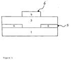
- a schematic cross-section of the cell is show, in Fig. 1.
- the polymer p-PPV was made by chemical synthesis (4).
- TiO 2 nanocrystals were obtained from Degussa AG corporation, Germany.
- An approximately 0.7% methanol solution of the p-PPV was combined with a colloid of TiO 2 made according to reference 5 to give a mixture of approximately 1:1 p-PPV and TiO 2 ,by weight.
- This mixture was spin-coated on a glass substrate 1 with a transparent conducting coating 2, in this example SnO2:F, to give a thin film 3.
- the film was heated to 320 °C for ten hours in vacuum and an aluminum contact 4 evaporated in such a way that there is no overlap with the transparent (with methods commonly known in the field), conducting coating on the glass on top of the film to complete
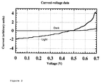
- the main novelty and crucial distinction of this method over other methods is the thermal treatment step, which is necessary for both conversion of the p-PPV to its final conducting form, PPV; and, to produce electrical contact between the TiO 2 particles to produce electron-carrying paths through the film.
- Our method is the first one to make operational photovoltaic cells of a conducting polymer, such as PPV, and a sintered electrically interconnected network of nanocrystalline particles, such as TiO 2 .
- PPV has been shown to be a good hole-conducting material (4) and TiO 2 an excellent electron transporter (1), so their combination together, prepared in a single thermal treatment step, also represents a significant advance.
- the method is general for a range of temperatures, other polymers, or nanocrystals.
Landscapes
- Chemical & Material Sciences (AREA)
- Engineering & Computer Science (AREA)
- Physics & Mathematics (AREA)
- Nanotechnology (AREA)
- Crystallography & Structural Chemistry (AREA)
- Optics & Photonics (AREA)
- Inorganic Chemistry (AREA)
- Electromagnetism (AREA)
- Life Sciences & Earth Sciences (AREA)
- Biophysics (AREA)
- Composite Materials (AREA)
- Condensed Matter Physics & Semiconductors (AREA)
- General Physics & Mathematics (AREA)
- Materials Engineering (AREA)
- Hybrid Cells (AREA)
- Photovoltaic Devices (AREA)
- Inorganic Compounds Of Heavy Metals (AREA)
Priority Applications (5)
| Application Number | Priority Date | Filing Date | Title |
|---|---|---|---|
| EP97203499A EP0917208A1 (de) | 1997-11-11 | 1997-11-11 | Optoelektronische Anordnung aus einem Polymer mit Nanokristallen und Herstellungsverfahren |
| US09/554,178 US6512172B1 (en) | 1997-11-11 | 1998-11-11 | Polymer-nanocrystal photo device and method for making the same |
| PCT/EP1998/007328 WO1999025028A1 (en) | 1997-11-11 | 1998-11-11 | Polymer-nanocrystal photo device and method for making the same |
| AU14355/99A AU1435599A (en) | 1997-11-11 | 1998-11-11 | Polymer-nanocrystal photo device and method for making the same |
| EP98958244A EP1029366A1 (de) | 1997-11-11 | 1998-11-11 | Optoelektronische vorrichtung aus einem polymer mit nanokristallen und herstellungsverfahren |
Applications Claiming Priority (1)
| Application Number | Priority Date | Filing Date | Title |
|---|---|---|---|
| EP97203499A EP0917208A1 (de) | 1997-11-11 | 1997-11-11 | Optoelektronische Anordnung aus einem Polymer mit Nanokristallen und Herstellungsverfahren |
Publications (1)
| Publication Number | Publication Date |
|---|---|
| EP0917208A1 true EP0917208A1 (de) | 1999-05-19 |
Family
ID=8228916
Family Applications (2)
| Application Number | Title | Priority Date | Filing Date |
|---|---|---|---|
| EP97203499A Withdrawn EP0917208A1 (de) | 1997-11-11 | 1997-11-11 | Optoelektronische Anordnung aus einem Polymer mit Nanokristallen und Herstellungsverfahren |
| EP98958244A Withdrawn EP1029366A1 (de) | 1997-11-11 | 1998-11-11 | Optoelektronische vorrichtung aus einem polymer mit nanokristallen und herstellungsverfahren |
Family Applications After (1)
| Application Number | Title | Priority Date | Filing Date |
|---|---|---|---|
| EP98958244A Withdrawn EP1029366A1 (de) | 1997-11-11 | 1998-11-11 | Optoelektronische vorrichtung aus einem polymer mit nanokristallen und herstellungsverfahren |
Country Status (4)
| Country | Link |
|---|---|
| US (1) | US6512172B1 (de) |
| EP (2) | EP0917208A1 (de) |
| AU (1) | AU1435599A (de) |
| WO (1) | WO1999025028A1 (de) |
Cited By (9)
| Publication number | Priority date | Publication date | Assignee | Title |
|---|---|---|---|---|
| GB2389230A (en) * | 2002-05-28 | 2003-12-03 | Univ Nat Taiwan | Nanoparticle light emitting device (LED) |
| FR2862429A1 (fr) * | 2003-11-17 | 2005-05-20 | Commissariat Energie Atomique | Materiau hybride inorganique-organique semi-conducteur p-n, son procede de fabrication et cellule photovoltaique comprenant ledit materiau |
| US7196333B1 (en) * | 1999-09-23 | 2007-03-27 | Commissariat A L'energie Atomique | Radiation detector using a composite material and method for making same |
| CN100366665C (zh) * | 2005-12-29 | 2008-02-06 | 复旦大学 | 光催化聚合制备无机半导体/导电聚合物复合薄膜的方法 |
| WO2011052511A1 (ja) * | 2009-10-29 | 2011-05-05 | 住友化学株式会社 | 有機光電変換素子 |
| WO2011015993A3 (en) * | 2009-08-07 | 2011-08-04 | Solargenius S.R.L. | Multilayer photovoltaic composition and method of application |
| CN103597286A (zh) * | 2011-06-06 | 2014-02-19 | 肖特公开股份有限公司 | 显示设备 |
| CN103915568A (zh) * | 2013-01-06 | 2014-07-09 | 吉林师范大学 | 一种CdS有机电致发光器件 |
| US9196847B2 (en) | 2005-12-23 | 2015-11-24 | Commissariat A L'energie Atomique | Sensitizing complexes, process for the preparation thereof, semiconductive inorganic/organic hybrid material comprising them, and photovoltaic cell comprising said material |
Families Citing this family (34)
| Publication number | Priority date | Publication date | Assignee | Title |
|---|---|---|---|---|
| EP1129496A2 (de) * | 1998-10-09 | 2001-09-05 | The Trustees of Columbia University in the City of New York | Photoelektrische festkörpervorrichtung |
| US20020110180A1 (en) * | 2001-02-09 | 2002-08-15 | Barney Alfred A. | Temperature-sensing composition |
| AU2002326920B2 (en) * | 2001-09-17 | 2007-09-13 | Massachusetts Institute Of Technology | Semiconductor nanocrystal composite |
| US7777303B2 (en) | 2002-03-19 | 2010-08-17 | The Regents Of The University Of California | Semiconductor-nanocrystal/conjugated polymer thin films |
| MY144626A (en) * | 2002-03-19 | 2011-10-14 | Univ California | Semiconductor-nanocrystal/conjugated polymer thin films |
| KR100495625B1 (ko) * | 2002-04-23 | 2005-06-16 | 대주전자재료 주식회사 | 유기 el 소자의 발광층용 공액성 고분자-무기물 나노복합체 조성물 |
| US20040126582A1 (en) * | 2002-08-23 | 2004-07-01 | Nano-Proprietary, Inc. | Silicon nanoparticles embedded in polymer matrix |
| EP1537187B1 (de) * | 2002-09-05 | 2012-08-15 | Nanosys, Inc. | Die ladungsübertragung auf oder von nanostrukturen erleichternde organische spezies |
| US7572393B2 (en) | 2002-09-05 | 2009-08-11 | Nanosys Inc. | Organic species that facilitate charge transfer to or from nanostructures |
| WO2004023527A2 (en) * | 2002-09-05 | 2004-03-18 | Nanosys, Inc. | Nanostructure and nanocomposite based compositions and photovoltaic devices |
| US7534488B2 (en) | 2003-09-10 | 2009-05-19 | The Regents Of The University Of California | Graded core/shell semiconductor nanorods and nanorod barcodes |
| EP1584114A1 (de) * | 2003-01-17 | 2005-10-12 | Diode Solutions, Inc. | Display mit einem organischen material |
| CN1309097C (zh) * | 2004-03-24 | 2007-04-04 | 武汉大学 | 提高TiO2光电池光电转换效率的方法 |
| DE102004030628A1 (de) * | 2004-06-24 | 2006-01-19 | Konarka Technologies, Inc., Lowell | Organisches elektronisches Element mit elektrisch leitfähiger semitransparenter Schicht |
| TWI271876B (en) * | 2005-05-27 | 2007-01-21 | Univ Nat Taiwan | Block copolymer containing nano-particles, electron transporting material and photoelectric device employing the same |
| US8835941B2 (en) * | 2006-02-09 | 2014-09-16 | Qd Vision, Inc. | Displays including semiconductor nanocrystals and methods of making same |
| KR100754396B1 (ko) * | 2006-02-16 | 2007-08-31 | 삼성전자주식회사 | 양자점 발광소자 및 그 제조방법 |
| WO2007143197A2 (en) * | 2006-06-02 | 2007-12-13 | Qd Vision, Inc. | Light-emitting devices and displays with improved performance |
| WO2007112088A2 (en) * | 2006-03-24 | 2007-10-04 | Qd Vision, Inc. | Hyperspectral imaging device |
| KR101061530B1 (ko) * | 2006-04-04 | 2011-09-01 | 6엔 실리콘 아이엔씨. | 실리콘의 정제 방법 |
| US20070254996A1 (en) * | 2006-04-28 | 2007-11-01 | Krzysztof Nauka | Nanocrystal-polymer composite materials and methods of attaching nanocrystals to polymer molecules |
| JP2010508620A (ja) * | 2006-09-12 | 2010-03-18 | キユーデイー・ビジヨン・インコーポレーテツド | 所定のパターンを表示するために有用なエレクトロルミネセントディスプレイ |
| US8222077B2 (en) * | 2006-11-07 | 2012-07-17 | Cbrite Inc. | Metal-insulator-metal (MIM) devices and their methods of fabrication |
| US9741901B2 (en) | 2006-11-07 | 2017-08-22 | Cbrite Inc. | Two-terminal electronic devices and their methods of fabrication |
| US7898042B2 (en) | 2006-11-07 | 2011-03-01 | Cbrite Inc. | Two-terminal switching devices and their methods of fabrication |
| WO2008063657A2 (en) * | 2006-11-21 | 2008-05-29 | Qd Vision, Inc. | Light emitting devices and displays with improved performance |
| KR101995369B1 (ko) | 2008-04-03 | 2019-07-02 | 삼성 리서치 아메리카 인코포레이티드 | 양자점들을 포함하는 발광 소자 |
| US9525148B2 (en) | 2008-04-03 | 2016-12-20 | Qd Vision, Inc. | Device including quantum dots |
| EP2403006A4 (de) * | 2009-02-27 | 2014-04-02 | Nat Inst For Materials Science | Pn-heteroübergangshalbleiter und herstellungsverfahren dafür |
| CN105931696B (zh) | 2010-04-23 | 2017-07-07 | 皮瑟莱根特科技有限责任公司 | 纳米晶体的合成、盖帽和分散 |
| US8920675B2 (en) | 2010-10-27 | 2014-12-30 | Pixelligent Technologies, Llc | Synthesis, capping and dispersion of nanocrystals |
| US9359689B2 (en) | 2011-10-26 | 2016-06-07 | Pixelligent Technologies, Llc | Synthesis, capping and dispersion of nanocrystals |
| CN108435260A (zh) * | 2018-03-26 | 2018-08-24 | 江苏奥净嘉环保科技有限公司 | 一种纳米二氧化钛硫化镉复合光催化剂的制备方法 |
| CN115483352A (zh) * | 2022-09-14 | 2022-12-16 | 暨南大学 | 一种大面积高质量钙钛矿薄膜的真空气相沉制备方法及利用该钙钛矿薄膜制备的光伏器件 |
Family Cites Families (2)
| Publication number | Priority date | Publication date | Assignee | Title |
|---|---|---|---|---|
| AU2492599A (en) * | 1998-02-02 | 1999-08-16 | Uniax Corporation | Organic diodes with switchable photosensitivity |
| EP1129496A2 (de) * | 1998-10-09 | 2001-09-05 | The Trustees of Columbia University in the City of New York | Photoelektrische festkörpervorrichtung |
-
1997
- 1997-11-11 EP EP97203499A patent/EP0917208A1/de not_active Withdrawn
-
1998
- 1998-11-11 WO PCT/EP1998/007328 patent/WO1999025028A1/en not_active Ceased
- 1998-11-11 US US09/554,178 patent/US6512172B1/en not_active Expired - Fee Related
- 1998-11-11 AU AU14355/99A patent/AU1435599A/en not_active Abandoned
- 1998-11-11 EP EP98958244A patent/EP1029366A1/de not_active Withdrawn
Non-Patent Citations (4)
| Title |
|---|
| KUCZKOWSKI A: "THE PROSPECTS FOR POLYESTER POLYMER-CDS POWER COMPOSITES IN PHOTOELECTRONIC DEVICE APPLICATIONS", JOURNAL OF PHYSICS D. APPLIED PHYSICS, vol. 22, no. 11, 14 November 1989 (1989-11-14), BRISTOL, GB, pages 1731 - 1735, XP000072966 * |
| N.C. GREENHAM ET AL.: "Charge separation and transport in conjugated polymer/cadmium selenide nanocrystal composites studied by photoluminescence quenching and photoconductivity", SYNTHETIC METALS, vol. 84, no. 1-3, 1 January 1997 (1997-01-01), AMSTERDAM, NL, pages 545 - 546, XP002060965 * |
| N.C. GREENHAM ET AL.: "Charge separation and transport in conjugated-polymer/semiconductor-nanocrystal composites studied by photoluminescence quenching and photoconductivity", PHYSICAL REVIEW, B. CONDENSED MATTER., vol. 54, no. 24, 15 December 1996 (1996-12-15), NEW YORK US, pages 17628 - 17637, XP002060964 * |
| S.A. CARTER ET AL.: "Enhanced luminance in polymer composite light emitting devices", APPLIED PHYSICS LETTERS., vol. 71, no. 9, 1 September 1997 (1997-09-01), NEW YORK US, pages 1145 - 1147, XP000720223 * |
Cited By (13)
| Publication number | Priority date | Publication date | Assignee | Title |
|---|---|---|---|---|
| US7196333B1 (en) * | 1999-09-23 | 2007-03-27 | Commissariat A L'energie Atomique | Radiation detector using a composite material and method for making same |
| GB2389230A (en) * | 2002-05-28 | 2003-12-03 | Univ Nat Taiwan | Nanoparticle light emitting device (LED) |
| FR2862429A1 (fr) * | 2003-11-17 | 2005-05-20 | Commissariat Energie Atomique | Materiau hybride inorganique-organique semi-conducteur p-n, son procede de fabrication et cellule photovoltaique comprenant ledit materiau |
| WO2005050752A1 (fr) * | 2003-11-17 | 2005-06-02 | Commissariat A L'energie Atomique | Materiau hybride inorganique-organique semi-conducteur p-n, son procede de fabrication et cellule photovoltaïque comprenant ledit materiau |
| US9196847B2 (en) | 2005-12-23 | 2015-11-24 | Commissariat A L'energie Atomique | Sensitizing complexes, process for the preparation thereof, semiconductive inorganic/organic hybrid material comprising them, and photovoltaic cell comprising said material |
| CN100366665C (zh) * | 2005-12-29 | 2008-02-06 | 复旦大学 | 光催化聚合制备无机半导体/导电聚合物复合薄膜的方法 |
| WO2011015993A3 (en) * | 2009-08-07 | 2011-08-04 | Solargenius S.R.L. | Multilayer photovoltaic composition and method of application |
| JP2011119697A (ja) * | 2009-10-29 | 2011-06-16 | Sumitomo Chemical Co Ltd | 有機光電変換素子 |
| WO2011052511A1 (ja) * | 2009-10-29 | 2011-05-05 | 住友化学株式会社 | 有機光電変換素子 |
| CN103597286A (zh) * | 2011-06-06 | 2014-02-19 | 肖特公开股份有限公司 | 显示设备 |
| CN103597286B (zh) * | 2011-06-06 | 2016-07-20 | 肖特公开股份有限公司 | 显示设备 |
| CN103915568A (zh) * | 2013-01-06 | 2014-07-09 | 吉林师范大学 | 一种CdS有机电致发光器件 |
| CN103915568B (zh) * | 2013-01-06 | 2016-07-20 | 吉林师范大学 | 一种CdS有机电致发光器件 |
Also Published As
| Publication number | Publication date |
|---|---|
| US6512172B1 (en) | 2003-01-28 |
| AU1435599A (en) | 1999-05-31 |
| EP1029366A1 (de) | 2000-08-23 |
| WO1999025028A1 (en) | 1999-05-20 |
Similar Documents
| Publication | Publication Date | Title |
|---|---|---|
| EP0917208A1 (de) | Optoelektronische Anordnung aus einem Polymer mit Nanokristallen und Herstellungsverfahren | |
| Zhang et al. | High-efficiency (> 20%) planar carbon-based perovskite solar cells through device configuration engineering | |
| Zhang et al. | Polymer photovoltaic cells with conducting polymer anodes | |
| O'Regan et al. | Electrodeposited nanocomposite n–p heterojunctions for solid‐state dye‐sensitized photovoltaics | |
| Khandelwal et al. | Semitransparent organic solar cells: from molecular design to structure–performance relationships | |
| Dou et al. | Perovskite‐based indoor photovoltaics and their competitors | |
| Suthar et al. | Indoor organic solar cells for low-power IoT devices: recent progress, challenges, and applications | |
| Lee et al. | Thin metal top electrode and interface engineering for efficient and air-stable semitransparent perovskite solar cells | |
| Zhao et al. | Metallic tin substitution of organic lead perovskite films for efficient solar cells | |
| Kim et al. | Nip-type perovskite solar cells employing n-type graphene transparent conductive electrodes | |
| Cho et al. | Efficient ITO-free semitransparent perovskite solar cells with metal transparent electrodes | |
| CN102142521A (zh) | 有机太阳能电池及其制备方法 | |
| US20230232705A1 (en) | Semi-transparent perovskite-based photovoltaic cells and process for preparing them | |
| Jiang et al. | Efficient perovskite indoor photovoltaics with open‐circuit voltage of 1.15 V via collaborative optimization of CsPbI2Br layer and hole transport layer | |
| Wang et al. | P3HT vs Spiro-OMeTAD as a hole transport layer for halide perovskite indoor photovoltaics and self-powering of motion sensors | |
| Ka et al. | Hysteresis‐Free 1D Network Mixed Halide‐Perovskite Semitransparent Solar Cells | |
| CN117440741A (zh) | 一种半透明钙钛矿太阳电池及其制备方法 | |
| KR101047396B1 (ko) | 유기 태양전지 및 그 제조 방법 | |
| KR101516474B1 (ko) | 은나노입자들을 포함하는 전도성 고분자 전극 기반의 플라즈몬 유기 광전자 디바이스 | |
| Yang et al. | Non‐Metallic Back Contacts for Indoor Perovskite Solar Cells: Material Criteria, Recent Progress, and Future Outlook | |
| Wang et al. | Efficient semitransparent bulk-heterojunction organic photovoltaic cells with high-performance low processing temperature indium–tin oxide top electrode | |
| Sun et al. | Advances in materials and devices for smartlife photovoltaic innovations | |
| Kang et al. | Fully vacuum‐free semitransparent polymer solar cells for power‐generating window with pure achromatic appealing | |
| US20240060827A1 (en) | Self-contained physical data sensor operating by the energy input from a photovoltaic module | |
| KR20250022032A (ko) | 페로브스카이트 기반 광전지 및 이를 제조하기 위한 공정 |
Legal Events
| Date | Code | Title | Description |
|---|---|---|---|
| PUAI | Public reference made under article 153(3) epc to a published international application that has entered the european phase |
Free format text: ORIGINAL CODE: 0009012 |
|
| AK | Designated contracting states |
Kind code of ref document: A1 Designated state(s): AT BE CH DE DK ES FI FR GB GR IE IT LI LU MC NL PT SE |
|
| AX | Request for extension of the european patent |
Free format text: AL;LT;LV;MK;RO;SI |
|
| AKX | Designation fees paid | ||
| REG | Reference to a national code |
Ref country code: DE Ref legal event code: 8566 |
|
| STAA | Information on the status of an ep patent application or granted ep patent |
Free format text: STATUS: THE APPLICATION IS DEEMED TO BE WITHDRAWN |
|
| 18D | Application deemed to be withdrawn |
Effective date: 19991120 |