EP0917412A2 - Circuit auto-oscillant avec circuit de démarrage simplifié - Google Patents
Circuit auto-oscillant avec circuit de démarrage simplifié Download PDFInfo
- Publication number
- EP0917412A2 EP0917412A2 EP98119611A EP98119611A EP0917412A2 EP 0917412 A2 EP0917412 A2 EP 0917412A2 EP 98119611 A EP98119611 A EP 98119611A EP 98119611 A EP98119611 A EP 98119611A EP 0917412 A2 EP0917412 A2 EP 0917412A2
- Authority
- EP
- European Patent Office
- Prior art keywords
- capacitor
- circuit
- operating circuit
- circuit according
- oscillator
- Prior art date
- Legal status (The legal status is an assumption and is not a legal conclusion. Google has not performed a legal analysis and makes no representation as to the accuracy of the status listed.)
- Granted
Links
Images


Classifications
-
- H—ELECTRICITY
- H05—ELECTRIC TECHNIQUES NOT OTHERWISE PROVIDED FOR
- H05B—ELECTRIC HEATING; ELECTRIC LIGHT SOURCES NOT OTHERWISE PROVIDED FOR; CIRCUIT ARRANGEMENTS FOR ELECTRIC LIGHT SOURCES, IN GENERAL
- H05B41/00—Circuit arrangements or apparatus for igniting or operating discharge lamps
- H05B41/14—Circuit arrangements
- H05B41/26—Circuit arrangements in which the lamp is fed by power derived from DC by means of a converter, e.g. by high-voltage DC
- H05B41/28—Circuit arrangements in which the lamp is fed by power derived from DC by means of a converter, e.g. by high-voltage DC using static converters
- H05B41/282—Circuit arrangements in which the lamp is fed by power derived from DC by means of a converter, e.g. by high-voltage DC using static converters with semiconductor devices
- H05B41/2825—Circuit arrangements in which the lamp is fed by power derived from DC by means of a converter, e.g. by high-voltage DC using static converters with semiconductor devices by means of a bridge converter in the final stage
-
- Y—GENERAL TAGGING OF NEW TECHNOLOGICAL DEVELOPMENTS; GENERAL TAGGING OF CROSS-SECTIONAL TECHNOLOGIES SPANNING OVER SEVERAL SECTIONS OF THE IPC; TECHNICAL SUBJECTS COVERED BY FORMER USPC CROSS-REFERENCE ART COLLECTIONS [XRACs] AND DIGESTS
- Y02—TECHNOLOGIES OR APPLICATIONS FOR MITIGATION OR ADAPTATION AGAINST CLIMATE CHANGE
- Y02B—CLIMATE CHANGE MITIGATION TECHNOLOGIES RELATED TO BUILDINGS, e.g. HOUSING, HOUSE APPLIANCES OR RELATED END-USER APPLICATIONS
- Y02B20/00—Energy efficient lighting technologies, e.g. halogen lamps or gas discharge lamps
-
- Y—GENERAL TAGGING OF NEW TECHNOLOGICAL DEVELOPMENTS; GENERAL TAGGING OF CROSS-SECTIONAL TECHNOLOGIES SPANNING OVER SEVERAL SECTIONS OF THE IPC; TECHNICAL SUBJECTS COVERED BY FORMER USPC CROSS-REFERENCE ART COLLECTIONS [XRACs] AND DIGESTS
- Y10—TECHNICAL SUBJECTS COVERED BY FORMER USPC
- Y10S—TECHNICAL SUBJECTS COVERED BY FORMER USPC CROSS-REFERENCE ART COLLECTIONS [XRACs] AND DIGESTS
- Y10S315/00—Electric lamp and discharge devices: systems
- Y10S315/05—Starting and operating circuit for fluorescent lamp
Definitions
- This invention relates to an operating circuit for a load in which an oscillator circuit a high-frequency power to supply the load generated.
- the oscillator circuit itself with a supply power supplied, e.g. B. a rectified network performance.
- a supply power supplied e.g. B. a rectified network performance.
- oscillator circuits with voltage-controlled switching elements considered, for example field-effect transistor half-bridges.
- Such operational circuits are mainly used in electronic ballasts for low pressure gas discharge lamps.
- This invention is based on the technical problem of an operating circuit of the type described above with an improved start-up circuit specify.
- the invention provides an operating circuit for a load, in particular a low-pressure gas discharge lamp, with a free-running oscillator with voltage-controlled switching elements to generate high-frequency output power for the load from a supply performance, which is characterized by a start-up circuit for starting the free-swinging oscillation with a between a control circuit a control terminal of a switching element and a reference potential of the Switching element switched starting capacitor.
- the invention is based on the knowledge that the im Prior art used diac a major disadvantage of the conventional Solution. It has been shown that Diacs in comparison to other components used in the operational circuits show an above-average high failure rate and thus to unnecessarily high ones Failure rates of the electronic ballasts equipped with them or other operating circuits.
- a capacitor is provided here is referred to as the starting capacitor.
- the starting capacitor has that Task, with increasing charging through its connection to a reference potential a switching element, for example to a power supply branch, a control circuit after switching on the power supply to enable the oscillator or one of its switching elements, to cause a first switching operation of the switching element in question.
- a switching element for example to a power supply branch
- a control circuit after switching on the power supply to enable the oscillator or one of its switching elements, to cause a first switching operation of the switching element in question.
- voltage-controlled Switching elements do not have very high currents, but only a certain one Tension is required.
- Have voltage controlled switching elements basically a defined one with regard to their switching on or off Threshold voltage.
- Control circuit can be provided in the minimal sense, so that the voltage applied to the starting capacitor acts practically directly on the control connection of the voltage-controlled switching element.
- a starting capacitor is according to the invention provided as a simple and inexpensive component, whereby the diac with the disadvantages described is superfluous.
- the oscillator is a half-bridge circuit, as is known in electronic ballasts.
- Preferred examples of voltage-controlled switching elements are in particular field effect transistors, especially MOSFETs, or IGBT ( Insulated Gate Bipolar Transistor ").
- the starting capacitor is simply charged via one between the starting capacitor and one suitable for charging Potential, such as a power supply branch, switched charging resistor, which should have a relatively high impedance, so that the start-up circuit little disturbance in oscillation mode, i.e. caused no asymmetry effects.
- one suitable for charging Potential such as a power supply branch, switched charging resistor, which should have a relatively high impedance, so that the start-up circuit little disturbance in oscillation mode, i.e. caused no asymmetry effects.
- the discharge resistor supports its discharge, especially when the oscillator is at a constant oscillation. It is particularly useful for increasing operational safety if a rectifier and a large electrolytic capacitor charged by it are used in network operation. This aspect relates to those operating phases in which the rectifier does not recharge the electrolytic capacitor and thus there is no potential coupling between the rectified side and the network side. In this Floating "state of the rectified side, the influence of displacement capacities in the rectifier can disrupt the potential conditions at a charging resistor connecting the network side and the rectified side and thus its discharge function.
- Another advantageous embodiment of the invention consists in a discharge diode for cyclical discharge of the starting capacitor in oscillation mode.
- This discharge diode is switched so that it is the actual Start-up process initially blocks and thus the charging of the starting capacitor allows. Is the free oscillation of the operating circuit first once started, step on the other connection side of the discharge diode with the oscillation frequency potential states on the starting capacitor Discharge cyclically via the discharge diode. With other potential states blocks the discharge diode. It is preferably between the control circuit side Connection of the starting capacitor and the supply branches remote Connection of the switching element in a bridge circuit a center tap of the bridge.
- Control circuit Two preferred variants, which have proven to be very suitable for reliable and low-loss operation, in particular of a half-bridge circuit, are the following:
- the control circuit of a series circuit comprising a resistor and a secondary winding of a control transformer is a parallel circuit consisting of a capacitor and a coil connected in parallel, the series circuit and the parallel circuit being connected together to the control connection of the switching element in question, the parallel circuit comprising the capacitor and the coil forming an oscillating circuit.
- the coil lying in parallel with the capacitor is omitted.
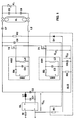
- FIG. 1 shows an operating circuit in an electronic ballast for a low-pressure gas discharge lamp, which is shown as load EL.
- a rectifier GL with mains voltage is used via a fuse SI supplied, which feeds an electrolytic capacitor C1 or keeps it live.
- Two supply branches are tapped at the electrolytic capacitor C1 via a filter from a coil L1 in one of the branches and one both Capacitor C2 connecting branches.
- the lower supply branch in the figure has negative potential and defines the reference potential on the rectified side of the operating circuit.
- the upper one is the positive supply branch.
- a half bridge made up of two MOSFET transistors is located in both supply branches T1 and T2, with N-channel transistors each with the negative Side source connector are used.
- a load circuit consisting of a load-series lamp choke L2, the low-pressure gas discharge lamp EL and the load serial coupling capacitor C7.
- control circuit AS1 or AS2 Between the source terminal of the MOSFET transistors T1 and T2 as internal transistor reference potential and the respective gate terminal one control circuit AS1 or AS2. With the lower half-bridge transistor T1 is the control circuit AS1, however, via the following Start-up circuit ALS described in more detail with the source connection of the Transistor T1 connected.
- the control circuits AS1 and AS2 are identical constructed and consist of a parallel connection of a coil L3 or L4, a capacitor C3 or C4 and a series connection of a secondary winding HW1 or HW2 of a control transformer, its primary winding the lamp choke already mentioned is L2, and a resistor R3 or R4.
- the winding sense of the secondary windings is - how indicated by the points on HW1, HW2 and L2 - opposite to each other.
- the start-up circuit with a dashed line ALS summarized, but basically also a resistance R2 between the center tap of the half-bridge and the positive Supply branch belongs.
- a starting capacitor C5 between the drive circuit AS1 of the lower one Bridge transistor T1 and the negative supply branch.
- a discharge resistor R5. Are in series with the starting capacitor C5 a discharge diode in connection with the center tap of the half-bridge D1 with its anode on the part of the starting capacitor C5, and a charging resistor R1 in connection to an AC voltage connection on the input side of the rectifier GL.
- the resistor R2 keeps the center tap of the half-bridge at the potential of the positive supply branch. This means that virtually the entire DC voltage of the electrolytic capacitor C1 is present at the lower bridge transistor T1. It is essential that the voltage U C5 on the starting capacitor C5 with the voltage of the drive circuit 1, that is the voltage on the capacitor C3, added between the source connection and the gate connection of the bridge transistor T1, is present in the figure as U GS .
- the control circuits AS1 and AS2 In the absence of positive feedback by the control transformer L2-HW1 / HW2 and in the absence of potential oscillation at the center of the half-bridge, the control circuits AS1 and AS2 initially do not give an output signal, so that the start-up circuit ALS must ensure a first switching operation.
- the bridge transistor T1 is switched on for the first time by charging the starting capacitor C5 via the charging resistor R1 on the part of a power supply line.
- the voltage U C5 on the starting capacitor C5 has reached the threshold voltage required for a first switch-on between the gate connection and the source connection of the bridge transistor T1 - at the beginning the voltages U C5 and U GS correspond because the control circuit AS1 is not active is - current flows through transistor T1 and the load circuit.
- the current in the lamp inductor L2 starts the positive feedback mechanism by generating an induction current in the secondary windings HW1 and HW2 in accordance with the turn ratio on this lamp inductor L2.
- the now conductive transistor T1 discharges together with the discharge diode D1 - the bridge center potential drops - the starting capacitor C5, however, the induction current in the secondary winding HW1 charges the capacitor C3 via the resistor R3 and thus keeps the transistor T1 switched on. If the first opening of the bridge transistor T1 by the voltage U C5 at the starting capacitor C5 has generated sufficient conductivity in the transistor T1, the free-oscillation now starts via the positive feedback mechanism and reaches a steady state over a few periods.
- the charging resistor R1 is connected to a mains lead on the input side of the rectifier GL. This has the following background: It is to be avoided with certainty that a state which is stationary over several mains half-waves, which can occur, for example, if the load current breaks off for a short time for reasons lying in the lamp EL and thus the positive feedback is interrupted at which the voltage U C5 is equal to the switch-on threshold voltage of the bridge transistor T1 and thus the total discharge current via the discharge diode D1 and the bridge transistor T1 is the current that charges the starting capacitor C5 and flows through the charging resistor R1 after reaching the steady state stands compensated.
- the starting process described above with reference to the circuit diagram in FIG. 1 is shown in another way in FIG. 2 by means of the gate-source voltage U GS of the transistor T1, the voltage U C5 at the starting capacitor C5, the current I T1 through the bridge transistor T1 ( over the switched route) and the current I L2 through the lamp choke L2.
- the time axis runs from left to right, and the deviating zero points for the voltages and currents are shown on the left edge of the figure.
- the charging process that is to say the rise in voltage U C5 over time
- the figure begins after a simultaneous increase in the voltages U C5 and U GS when the switch-on threshold voltage of the transistor T1 is exceeded, which is expressed in the sudden increase in the current I T1 .
- the short current peak results from the rapid charging of the switching relief capacitor C6, but the rise in I T1 continues afterwards.
- the rise in the transistor current I T1 is reflected to a certain extent in a dip in the voltage U C5.
- the diagram in FIG. 2 shows how the lamp inductor current I L2 is started when the conductivity of the transistor T1 begins, that is to say by I T1 .
- the positive feedback mechanism described already leads to a start of the activity of the control circuits when the transistor current I T1 rises, ie the transistor T1 is switched off again by the control circuit AS1 and the transistor T2 is then switched on by the control circuit AS2. Accordingly, the voltage U GS on the transistor T1 swings through to negative values, which in turn manifests itself in the beginning oscillation of the lamp inductor current I L2 . In the further course of time, oscillations oscillating both of the voltage U GS and of the load or lamp inductor current I L2 can be seen .
- the second dip in the voltage U C5 at the starting capacitor C5 is significantly stronger than the first, albeit of a similar quality.
- the quantitative increase in the effect is due to the much clearer conductivity of the bridge transistor T1 in the second or first switch-on process purely caused by the positive feedback mechanism.
- the potential of the center of the bridge falls below the reference potential of the negative supply branch, specifically because of the forward voltage of the body diode of the MOSFET T1, which must now conduct the considerable current flow from the lamp inductor L2.
- the second embodiment whose Circuit diagram shown in Figure 3.
- the differences from the circuit Figure 1 are as follows:
- the bridge transistor T2 is now a P-channel MOSFET instead of the previous N-channel MOSFET.
- the resistance is accordingly R2 now between the bridge center and the negative Supply branch.
- the control circuit AS2 is not at the bridge center but connected to the positive, upper supply branch.
- the charging resistance R1 is present here the other mains lead.
- the polarity of the discharge diode D1 is adjusted, vice versa.
- capacitor C6 is also between the bridge center and the lower, i.e. negative supply branch; however, it could just as well be in the old place.
- the Functioning otherwise corresponds to that described above and will not explained again here.
- control circuits AS1 and AS2 also from a parallel connection of only one capacitor C3, C4 and a series connection of a resistor R3, R4 and a secondary winding HW1, HW2 of a control transformer, its primary winding the lamp choke listed above is L2. Otherwise the circuit structure is identical to the circuit shown in FIG. 1.
Landscapes
- Circuit Arrangements For Discharge Lamps (AREA)
- Inverter Devices (AREA)
Applications Claiming Priority (2)
| Application Number | Priority Date | Filing Date | Title |
|---|---|---|---|
| DE19751063A DE19751063A1 (de) | 1997-11-18 | 1997-11-18 | Freischwingende Oszillatorschaltung mit einfacher Anlaufschaltung |
| DE19751063 | 1997-11-18 |
Publications (3)
| Publication Number | Publication Date |
|---|---|
| EP0917412A2 true EP0917412A2 (fr) | 1999-05-19 |
| EP0917412A3 EP0917412A3 (fr) | 1999-07-28 |
| EP0917412B1 EP0917412B1 (fr) | 2003-02-26 |
Family
ID=7849082
Family Applications (1)
| Application Number | Title | Priority Date | Filing Date |
|---|---|---|---|
| EP98119611A Expired - Lifetime EP0917412B1 (fr) | 1997-11-18 | 1998-10-16 | Circuit auto-oscillant avec circuit de démarrage simplifié |
Country Status (7)
| Country | Link |
|---|---|
| US (1) | US6246173B1 (fr) |
| EP (1) | EP0917412B1 (fr) |
| JP (1) | JP4216934B2 (fr) |
| KR (1) | KR100596950B1 (fr) |
| CN (1) | CN1196380C (fr) |
| CA (1) | CA2254392A1 (fr) |
| DE (2) | DE19751063A1 (fr) |
Cited By (5)
| Publication number | Priority date | Publication date | Assignee | Title |
|---|---|---|---|---|
| ES2156742A1 (es) * | 1999-06-21 | 2001-07-01 | Univ Oviedo | Balasto electronico de bajo coste y correccion activa del factor de potencia. |
| WO2009010091A1 (fr) * | 2007-07-16 | 2009-01-22 | Osram Gesellschaft mit beschränkter Haftung | Montage et procédé pour faire fonctionner une lampe à décharge |
| US7560874B2 (en) | 2006-09-30 | 2009-07-14 | Osram Sylvania Inc. | Electronic ballast with improved inverter startup circuit |
| EP2268108A1 (fr) * | 2009-06-22 | 2010-12-29 | Osram Gesellschaft mit Beschränkter Haftung | Convertisseur pour alimenter des sources lumineuses, méthode et support associés. |
| US7888879B2 (en) | 2005-07-14 | 2011-02-15 | Osram Gesellschaft Mit Beschaenkter Haftung | Circuit arrangement and method for operating at least one electric lamp |
Families Citing this family (11)
| Publication number | Priority date | Publication date | Assignee | Title |
|---|---|---|---|---|
| DE60143805D1 (de) * | 2000-10-31 | 2011-02-17 | Osram Sylvania Inc | Ballast-selbstoszillationswechselrichter mit phasengeregelter spannungsrückkopplung |
| DE10160790A1 (de) * | 2001-01-12 | 2002-08-08 | Patent Treuhand Ges Fuer Elektrische Gluehlampen Mbh | Schaltungsanordnung zum Einschalten einer Teilschaltungsanordnung |
| JP2002299097A (ja) * | 2001-03-30 | 2002-10-11 | Mitsubishi Electric Corp | 放電灯点灯装置 |
| JP2002299096A (ja) * | 2001-03-30 | 2002-10-11 | Mitsubishi Electric Corp | 放電灯点灯装置 |
| DE10235217A1 (de) * | 2002-08-01 | 2004-02-19 | Patent-Treuhand-Gesellschaft für elektrische Glühlampen mbH | Schaltungsvorrichtung und Verfahren zum Betreiben einer Lampe |
| JP2006172749A (ja) * | 2004-12-13 | 2006-06-29 | Ushio Inc | ランプ点灯回路 |
| DE102005025154A1 (de) * | 2005-06-01 | 2006-12-07 | Patent-Treuhand-Gesellschaft für elektrische Glühlampen mbH | Schaltungsanordnung zum Betrieb einer Entladungslampe mit Temperaturausgleich |
| US8699244B1 (en) | 2010-10-29 | 2014-04-15 | Universal Lighting Technologies, Inc. | Electronic ballast with load-independent and self-oscillating inverter topology |
| JP6221833B2 (ja) * | 2014-02-28 | 2017-11-01 | 株式会社島津製作所 | 高周波発振回路 |
| CN106499973B (zh) * | 2016-10-28 | 2023-06-20 | 邓树兴 | 双端供电安全隔离的电子兼容型led灯管及供电模块 |
| EP4525247A1 (fr) * | 2023-09-15 | 2025-03-19 | Siemens Energy Global GmbH & Co. KG | Alimentation électrique rapidement déénergisable pour un système d'électrolyse |
Family Cites Families (11)
| Publication number | Priority date | Publication date | Assignee | Title |
|---|---|---|---|---|
| NL8503008A (nl) * | 1985-11-04 | 1987-06-01 | Philips Nv | Gelijkstroom-wisselstroomomzetter voor het ontsteken en voeden van een ontladingslamp. |
| US4745537A (en) * | 1987-01-23 | 1988-05-17 | Cheung P S | Low dissipation power converter |
| US5262699A (en) * | 1991-08-26 | 1993-11-16 | Gte Products Corporation | Starting and operating circuit for arc discharge lamp |
| DE4129430A1 (de) | 1991-09-04 | 1993-03-11 | Patent Treuhand Ges Fuer Elektrische Gluehlampen Mbh | Schaltungsanordnung zum betrieb einer lampe |
| US5140225A (en) * | 1991-10-15 | 1992-08-18 | Barton Daniel W | High frequency lamp transformer for linear lighting fixture |
| JP2833998B2 (ja) * | 1994-06-06 | 1998-12-09 | 日本電気精器株式会社 | 高周波電力の非接触給電装置 |
| US5574335A (en) * | 1994-08-02 | 1996-11-12 | Osram Sylvania Inc. | Ballast containing protection circuit for detecting rectification of arc discharge lamp |
| DE19548506A1 (de) * | 1995-12-22 | 1997-06-26 | Patent Treuhand Ges Fuer Elektrische Gluehlampen Mbh | Schaltungsanordnung zum Betrieb einer Lampe |
| DE19612170A1 (de) * | 1996-03-27 | 1997-10-02 | Patent Treuhand Ges Fuer Elektrische Gluehlampen Mbh | Schaltungsanordnung zum Betrieb von elektrischen Lampen und Betriebsverfahren für elektrische Lampen |
| US5892327A (en) * | 1996-04-06 | 1999-04-06 | U.S. Philips Corporation | Circuit arrangement for operating a discharge lamp |
| JP3821454B2 (ja) * | 1996-07-12 | 2006-09-13 | 松下電器産業株式会社 | 蛍光ランプ点灯装置 |
-
1997
- 1997-11-18 DE DE19751063A patent/DE19751063A1/de not_active Withdrawn
-
1998
- 1998-10-16 DE DE59807298T patent/DE59807298D1/de not_active Expired - Lifetime
- 1998-10-16 EP EP98119611A patent/EP0917412B1/fr not_active Expired - Lifetime
- 1998-11-17 US US09/193,223 patent/US6246173B1/en not_active Expired - Lifetime
- 1998-11-17 CA CA002254392A patent/CA2254392A1/fr not_active Abandoned
- 1998-11-17 JP JP32626498A patent/JP4216934B2/ja not_active Expired - Fee Related
- 1998-11-18 KR KR1019980049373A patent/KR100596950B1/ko not_active Expired - Fee Related
- 1998-11-18 CN CNB98122413XA patent/CN1196380C/zh not_active Expired - Fee Related
Cited By (5)
| Publication number | Priority date | Publication date | Assignee | Title |
|---|---|---|---|---|
| ES2156742A1 (es) * | 1999-06-21 | 2001-07-01 | Univ Oviedo | Balasto electronico de bajo coste y correccion activa del factor de potencia. |
| US7888879B2 (en) | 2005-07-14 | 2011-02-15 | Osram Gesellschaft Mit Beschaenkter Haftung | Circuit arrangement and method for operating at least one electric lamp |
| US7560874B2 (en) | 2006-09-30 | 2009-07-14 | Osram Sylvania Inc. | Electronic ballast with improved inverter startup circuit |
| WO2009010091A1 (fr) * | 2007-07-16 | 2009-01-22 | Osram Gesellschaft mit beschränkter Haftung | Montage et procédé pour faire fonctionner une lampe à décharge |
| EP2268108A1 (fr) * | 2009-06-22 | 2010-12-29 | Osram Gesellschaft mit Beschränkter Haftung | Convertisseur pour alimenter des sources lumineuses, méthode et support associés. |
Also Published As
| Publication number | Publication date |
|---|---|
| DE59807298D1 (de) | 2003-04-03 |
| JPH11252933A (ja) | 1999-09-17 |
| EP0917412B1 (fr) | 2003-02-26 |
| KR100596950B1 (ko) | 2006-08-30 |
| KR19990045363A (ko) | 1999-06-25 |
| CN1220572A (zh) | 1999-06-23 |
| US6246173B1 (en) | 2001-06-12 |
| DE19751063A1 (de) | 1999-05-20 |
| CN1196380C (zh) | 2005-04-06 |
| CA2254392A1 (fr) | 1999-05-18 |
| EP0917412A3 (fr) | 1999-07-28 |
| JP4216934B2 (ja) | 2009-01-28 |
Similar Documents
| Publication | Publication Date | Title |
|---|---|---|
| EP0264765B1 (fr) | Disposition de circuit pour la mise en oeuvre de lampe à incandescence halogène basse tension | |
| DE19506977C2 (de) | Gate-Treiberschaltung | |
| EP0917412B1 (fr) | Circuit auto-oscillant avec circuit de démarrage simplifié | |
| EP0852454B1 (fr) | Circuit pour alimenter une lampe à décharge basse pression sans électrodes | |
| DE3527622A1 (de) | Vorschaltanordnung fuer eine leuchtstofflampe | |
| DE4332059A1 (de) | Lichtsteuervorrichtung für eine Entladungslampe | |
| DE19813187A1 (de) | Stromversorgungseinrichtung | |
| EP0062276B1 (fr) | Ballast pour le fonctionnement de lampes à décharge à basse pression | |
| DE102005007346A1 (de) | Schaltungsanordnung und Verfahren zum Betreiben von Gasentladungslampen | |
| DE69315761T2 (de) | Geschützter Umrichter zur Steuerung einer Entladungslampe | |
| EP0439240B1 (fr) | Ballast électronique | |
| DE69029301T2 (de) | Anzündanordnung für eine entladungslampe | |
| DE19729768B4 (de) | Schaltungsanordnung zum Zünden und Betreiben einer Leuchtstofflampe | |
| DE3711814C2 (de) | Elektronisches Vorschaltgerät zum Betrieb von Leuchtstofflampen | |
| DE69224097T2 (de) | Schaltungsanordnung | |
| DE4005776C2 (de) | Schaltungsanordnung zum Starten und zum Betrieb einer Gasentladungslampe | |
| EP1289350B1 (fr) | Circuit de commande pour lampe à décharge avec électrodes préchauffées | |
| EP1326484B1 (fr) | Appareil pour alimenter des lampes à décharge | |
| DE3342010A1 (de) | Wechselrichterschaltung | |
| EP0697803A2 (fr) | Circuit pour alimenter des lampes à décharge | |
| EP1282342B1 (fr) | Cicuit auto-oscillant | |
| WO2009010091A1 (fr) | Montage et procédé pour faire fonctionner une lampe à décharge | |
| EP1517592B1 (fr) | Circuit pour produire une tension alternative d'une tension continue | |
| EP1813135A1 (fr) | Circuit pour faire fonctionner une lampe a decharge a haute pression | |
| DE3736800C2 (fr) |
Legal Events
| Date | Code | Title | Description |
|---|---|---|---|
| PUAI | Public reference made under article 153(3) epc to a published international application that has entered the european phase |
Free format text: ORIGINAL CODE: 0009012 |
|
| AK | Designated contracting states |
Kind code of ref document: A2 Designated state(s): BE DE FR GB IT NL SE |
|
| AX | Request for extension of the european patent |
Free format text: AL;LT;LV;MK;RO;SI |
|
| PUAL | Search report despatched |
Free format text: ORIGINAL CODE: 0009013 |
|
| AK | Designated contracting states |
Kind code of ref document: A3 Designated state(s): AT BE CH CY DE DK ES FI FR GB GR IE IT LI LU MC NL PT SE |
|
| AX | Request for extension of the european patent |
Free format text: AL;LT;LV;MK;RO;SI |
|
| RIC1 | Information provided on ipc code assigned before grant |
Free format text: 6H 05B 41/29 A, 6H 02M 7/5383 B |
|
| 17P | Request for examination filed |
Effective date: 19990820 |
|
| AKX | Designation fees paid |
Free format text: BE DE FR GB IT NL SE |
|
| 17Q | First examination report despatched |
Effective date: 20000225 |
|
| RIC1 | Information provided on ipc code assigned before grant |
Free format text: 7H 05B 41/282 A, 7H 02M 7/5383 B |
|
| GRAH | Despatch of communication of intention to grant a patent |
Free format text: ORIGINAL CODE: EPIDOS IGRA |
|
| GRAH | Despatch of communication of intention to grant a patent |
Free format text: ORIGINAL CODE: EPIDOS IGRA |
|
| GRAA | (expected) grant |
Free format text: ORIGINAL CODE: 0009210 |
|
| AK | Designated contracting states |
Designated state(s): BE DE FR GB IT NL SE |
|
| REG | Reference to a national code |
Ref country code: GB Ref legal event code: FG4D Free format text: NOT ENGLISH |
|
| REF | Corresponds to: |
Ref document number: 59807298 Country of ref document: DE Date of ref document: 20030403 Kind code of ref document: P |
|
| REG | Reference to a national code |
Ref country code: SE Ref legal event code: TRGR |
|
| GBT | Gb: translation of ep patent filed (gb section 77(6)(a)/1977) | ||
| ET | Fr: translation filed | ||
| PLBE | No opposition filed within time limit |
Free format text: ORIGINAL CODE: 0009261 |
|
| STAA | Information on the status of an ep patent application or granted ep patent |
Free format text: STATUS: NO OPPOSITION FILED WITHIN TIME LIMIT |
|
| 26N | No opposition filed |
Effective date: 20031127 |
|
| PGFP | Annual fee paid to national office [announced via postgrant information from national office to epo] |
Ref country code: NL Payment date: 20061006 Year of fee payment: 9 |
|
| PGFP | Annual fee paid to national office [announced via postgrant information from national office to epo] |
Ref country code: SE Payment date: 20061012 Year of fee payment: 9 |
|
| PGFP | Annual fee paid to national office [announced via postgrant information from national office to epo] |
Ref country code: BE Payment date: 20061019 Year of fee payment: 9 |
|
| BERE | Be: lapsed |
Owner name: *PATENT-TREUHAND-G.- FUR ELEKTRISCHE GLUHLAMPEN M. Effective date: 20071031 |
|
| EUG | Se: european patent has lapsed | ||
| NLV4 | Nl: lapsed or anulled due to non-payment of the annual fee |
Effective date: 20080501 |
|
| PG25 | Lapsed in a contracting state [announced via postgrant information from national office to epo] |
Ref country code: BE Free format text: LAPSE BECAUSE OF NON-PAYMENT OF DUE FEES Effective date: 20071031 |
|
| PG25 | Lapsed in a contracting state [announced via postgrant information from national office to epo] |
Ref country code: SE Free format text: LAPSE BECAUSE OF NON-PAYMENT OF DUE FEES Effective date: 20071017 Ref country code: NL Free format text: LAPSE BECAUSE OF NON-PAYMENT OF DUE FEES Effective date: 20080501 |
|
| REG | Reference to a national code |
Ref country code: DE Ref legal event code: R081 Ref document number: 59807298 Country of ref document: DE Owner name: OSRAM GMBH, DE Free format text: FORMER OWNER: OSRAM GESELLSCHAFT MIT BESCHRAENKTER HAFTUNG, 81543 MUENCHEN, DE Effective date: 20111130 |
|
| PGFP | Annual fee paid to national office [announced via postgrant information from national office to epo] |
Ref country code: FR Payment date: 20121031 Year of fee payment: 15 |
|
| PGFP | Annual fee paid to national office [announced via postgrant information from national office to epo] |
Ref country code: IT Payment date: 20121022 Year of fee payment: 15 Ref country code: GB Payment date: 20121019 Year of fee payment: 15 |
|
| REG | Reference to a national code |
Ref country code: DE Ref legal event code: R081 Ref document number: 59807298 Country of ref document: DE Owner name: OSRAM GMBH, DE Free format text: FORMER OWNER: OSRAM AG, 81543 MUENCHEN, DE Effective date: 20130205 |
|
| REG | Reference to a national code |
Ref country code: DE Ref legal event code: R081 Ref document number: 59807298 Country of ref document: DE Owner name: OSRAM GMBH, DE Free format text: FORMER OWNER: OSRAM GMBH, 81543 MUENCHEN, DE Effective date: 20130822 |
|
| GBPC | Gb: european patent ceased through non-payment of renewal fee |
Effective date: 20131016 |
|
| PG25 | Lapsed in a contracting state [announced via postgrant information from national office to epo] |
Ref country code: GB Free format text: LAPSE BECAUSE OF NON-PAYMENT OF DUE FEES Effective date: 20131016 |
|
| REG | Reference to a national code |
Ref country code: FR Ref legal event code: ST Effective date: 20140630 |
|
| PG25 | Lapsed in a contracting state [announced via postgrant information from national office to epo] |
Ref country code: FR Free format text: LAPSE BECAUSE OF NON-PAYMENT OF DUE FEES Effective date: 20131031 Ref country code: IT Free format text: LAPSE BECAUSE OF NON-PAYMENT OF DUE FEES Effective date: 20131016 |
|
| PGFP | Annual fee paid to national office [announced via postgrant information from national office to epo] |
Ref country code: DE Payment date: 20141022 Year of fee payment: 17 |
|
| REG | Reference to a national code |
Ref country code: DE Ref legal event code: R119 Ref document number: 59807298 Country of ref document: DE |
|
| PG25 | Lapsed in a contracting state [announced via postgrant information from national office to epo] |
Ref country code: DE Free format text: LAPSE BECAUSE OF NON-PAYMENT OF DUE FEES Effective date: 20160503 |