EP0917412B1 - Freischwingende Oszillatorschaltung mit einfacher Anlaufschaltung - Google Patents
Freischwingende Oszillatorschaltung mit einfacher Anlaufschaltung Download PDFInfo
- Publication number
- EP0917412B1 EP0917412B1 EP98119611A EP98119611A EP0917412B1 EP 0917412 B1 EP0917412 B1 EP 0917412B1 EP 98119611 A EP98119611 A EP 98119611A EP 98119611 A EP98119611 A EP 98119611A EP 0917412 B1 EP0917412 B1 EP 0917412B1
- Authority
- EP
- European Patent Office
- Prior art keywords
- circuit
- capacitor
- bridge
- transistor
- resistor
- Prior art date
- Legal status (The legal status is an assumption and is not a legal conclusion. Google has not performed a legal analysis and makes no representation as to the accuracy of the status listed.)
- Expired - Lifetime
Links
- 239000003990 capacitor Substances 0.000 claims description 66
- 230000010355 oscillation Effects 0.000 claims description 16
- 238000004804 winding Methods 0.000 claims description 13
- 230000005669 field effect Effects 0.000 claims description 9
- 238000000034 method Methods 0.000 description 9
- 238000010586 diagram Methods 0.000 description 7
- 230000009024 positive feedback mechanism Effects 0.000 description 5
- 230000000694 effects Effects 0.000 description 3
- 230000006698 induction Effects 0.000 description 3
- 238000007599 discharging Methods 0.000 description 2
- 230000015556 catabolic process Effects 0.000 description 1
- 230000008878 coupling Effects 0.000 description 1
- 238000010168 coupling process Methods 0.000 description 1
- 238000005859 coupling reaction Methods 0.000 description 1
- 230000007246 mechanism Effects 0.000 description 1
Images


Classifications
-
- H—ELECTRICITY
- H05—ELECTRIC TECHNIQUES NOT OTHERWISE PROVIDED FOR
- H05B—ELECTRIC HEATING; ELECTRIC LIGHT SOURCES NOT OTHERWISE PROVIDED FOR; CIRCUIT ARRANGEMENTS FOR ELECTRIC LIGHT SOURCES, IN GENERAL
- H05B41/00—Circuit arrangements or apparatus for igniting or operating discharge lamps
- H05B41/14—Circuit arrangements
- H05B41/26—Circuit arrangements in which the lamp is fed by power derived from DC by means of a converter, e.g. by high-voltage DC
- H05B41/28—Circuit arrangements in which the lamp is fed by power derived from DC by means of a converter, e.g. by high-voltage DC using static converters
- H05B41/282—Circuit arrangements in which the lamp is fed by power derived from DC by means of a converter, e.g. by high-voltage DC using static converters with semiconductor devices
- H05B41/2825—Circuit arrangements in which the lamp is fed by power derived from DC by means of a converter, e.g. by high-voltage DC using static converters with semiconductor devices by means of a bridge converter in the final stage
-
- Y—GENERAL TAGGING OF NEW TECHNOLOGICAL DEVELOPMENTS; GENERAL TAGGING OF CROSS-SECTIONAL TECHNOLOGIES SPANNING OVER SEVERAL SECTIONS OF THE IPC; TECHNICAL SUBJECTS COVERED BY FORMER USPC CROSS-REFERENCE ART COLLECTIONS [XRACs] AND DIGESTS
- Y02—TECHNOLOGIES OR APPLICATIONS FOR MITIGATION OR ADAPTATION AGAINST CLIMATE CHANGE
- Y02B—CLIMATE CHANGE MITIGATION TECHNOLOGIES RELATED TO BUILDINGS, e.g. HOUSING, HOUSE APPLIANCES OR RELATED END-USER APPLICATIONS
- Y02B20/00—Energy efficient lighting technologies, e.g. halogen lamps or gas discharge lamps
-
- Y—GENERAL TAGGING OF NEW TECHNOLOGICAL DEVELOPMENTS; GENERAL TAGGING OF CROSS-SECTIONAL TECHNOLOGIES SPANNING OVER SEVERAL SECTIONS OF THE IPC; TECHNICAL SUBJECTS COVERED BY FORMER USPC CROSS-REFERENCE ART COLLECTIONS [XRACs] AND DIGESTS
- Y10—TECHNICAL SUBJECTS COVERED BY FORMER USPC
- Y10S—TECHNICAL SUBJECTS COVERED BY FORMER USPC CROSS-REFERENCE ART COLLECTIONS [XRACs] AND DIGESTS
- Y10S315/00—Electric lamp and discharge devices: systems
- Y10S315/05—Starting and operating circuit for fluorescent lamp
Definitions
- This invention relates to an operating circuit for a low pressure gas discharge lamp with a rectifier, with a free-swinging half bridge with voltage controlled field effect or IGBT transistors for generation a high frequency output power for the low pressure gas discharge lamp a supply power and with a start-up circuit for starting the free-swinging Oscillation with one between a drive circuit on one Control connection of a field effect or IGBT transistor and a reference potential of the field effect or IGBT transistor switched starting capacitor.
- Diacs compared to other components used in the operational circuits an above average show high failure rates and thus unnecessarily high failure rates of the electronic ballasts or other operating circuits equipped with them to lead.
- the starting capacitor does the job with increasing charging through its connector to a reference potential of a switching element, such as a power supply branch, after switching on the power supply a control circuit of the To enable the oscillator or one of its switching elements, a first Switching operation of the relevant switching element.
- a switching element such as a power supply branch
- a first Switching operation of the relevant switching element is the case with voltage-controlled switching elements no very high currents, just a certain voltage is required.
- Voltage-controlled switching elements have with regard to their switching on or off basically a defined threshold voltage.
- the diode with your Breakthrough process, which the invention is intended to avoid, as explained, can therefore be replaced are approached by and exceeding the voltage threshold of the switching element. This process is accomplished by switching on the power supply charging starting capacitor directly or indirectly.
- Charging the starting capacitor should be easy via one between the starting capacitor and a potential suitable for charging, such as a power supply branch, switched charging resistor take place, the relatively high resistance should be dimensioned so that the start-up circuit interferes little in oscillation mode.
- a corresponding circuit is known from US Pat. No. 5,592,367, in which the charging resistor is connected on the DC side of the rectifier bridge. at However, this circuit may have a current flowing across the charging resistor with a current-carrying connection of the FET transistor connecting diode and the still slightly conductive FET transistor that flows exactly over the current compensated for the starting capacitor. In this case, the current can flow through the starting capacitor no longer bring the FET transistor into the conductive state, so that a new starting process of the circuit arrangement only due to an interruption in the network can be achieved.
- the object of the invention is therefore this disadvantage through an improved start-up circuit to get around.
- the invention provides an operating circuit for a low-pressure gas discharge lamp with the features listed in the preamble of claim 1 before, which is characterized by a between the starting capacitor and a mains input side of the rectifier switched charging resistor and one discharge resistor connected in parallel with the starting capacitor.
- From US 5 140 225 is the connection of a starting circuit via a resistor known on the AC side of the rectifier.
- connections are supposed to be the power loss during charging of the starting capacitor be reduced.
- the starting capacitor connected in parallel in the circuit arrangement from US Pat. No. 5,592,367 Diode cannot contribute to the discharge resistor connected in parallel be compared to the present circuit because the diode has the wrong polarity for discharging the starting capacitor.
- An advantageous embodiment of the invention consists in a discharge diode for cyclical discharge of the starting capacitor in oscillation mode. Is the free-swinging Once the oscillation of the operating circuit has started, step on on the other connection side of the discharge diode with the oscillation frequency Potential states on the starting capacitor cyclically via the discharge diode discharged.
- the discharge diode blocks in other potential states. It is preferred between the control circuit side connection of the starting capacitor and the connection of the switching element remote from the supply branch, in the case of a bridge circuit a center tap of the bridge.
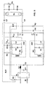
- FIG. 1 shows an operating circuit in an electronic ballast for a low-pressure gas discharge lamp, which is shown as load EL.
- a rectifier GL with mains voltage is used via a fuse SI supplied, which feeds an electrolytic capacitor C1 or keeps it live.
- Two supply branches are tapped at the electrolytic capacitor C1 via a filter from a coil L1 in one of the branches and one both Capacitor C2 connecting branches.
- the lower supply branch in the figure has negative potential and defines the reference potential on the rectified side of the operating circuit.
- the upper is the supply branch that is positive.
- a half bridge made up of two MOSFET transistors is located in both supply branches T1 and T2, with N-channel transistors each on the negative Side source connector are used.
- a load circuit consisting of a load series lamp choke L2, the low pressure gas discharge lamp EL and the load serial coupling capacitor C7.
- control circuit AS1 or AS2 Between the source terminal of the MOSFET transistors T1 and T2 as internal transistor reference potential and the respective gate terminal one control circuit AS1 or AS2. With the lower half-bridge transistor T1 is the control circuit AS1, however, via the following Start-up circuit ALS described in more detail with the source connection of the Transistor T1 connected.
- the control circuits AS1 and AS2 are identical constructed and consist of a parallel connection of a coil L3 or L4, a capacitor C3 or C4 and a series connection of a secondary winding HW1 or HW2 of a control transformer, its primary winding the lamp choke already mentioned is L2, and a resistor R3 or R4.
- the winding sense of the secondary windings is - how indicated by the points on HW1, HW2 and L2 - opposite to each other.
- the starting circuit In the lower area in FIG. 1 is the starting circuit with a dashed line ALS summarized, but basically also a resistance R2 between the center tap of the half-bridge and the positive Supply branch belongs.
- a starting capacitor C5 In the start-up circuit is initially a starting capacitor C5 between the drive circuit AS1 of the lower one Bridge transistor T1 and the negative supply branch.
- a discharge resistor R5. Are in series with the starting capacitor C5 a discharge diode in connection with the center tap of the half-bridge D1 with its anode on the part of the starting capacitor C5, and a charging resistor R1 in connection with an AC voltage connection on the input side of the rectifier GL.
- the resistor R2 keeps the center tap of the half-bridge at the potential of the positive supply branch. This means that virtually the entire DC voltage of the electrolytic capacitor C1 is present at the lower bridge transistor T1. It is essential that the voltage U C5 on the starting capacitor C5 with the voltage of the drive circuit 1, that is the voltage on the capacitor C3, added between the source connection and the gate connection of the bridge transistor T1, is present in the figure as U GS .
- the control circuits AS1 and AS2 In the absence of positive feedback by the control transformer L2-HW1 / HW2 and in the absence of potential oscillation at the center of the half-bridge, the control circuits AS1 and AS2 initially do not give an output signal, so that the start-up circuit ALS must take care of a first switching operation.
- the bridge transistor T1 is switched on for the first time by charging the starting capacitor C5 via the charging resistor R1 on the part of a power supply line.
- the current in the lamp inductor L2 starts the positive feedback mechanism by generating an induction current in the secondary windings HW1 and HW2 in accordance with the turn ratio on this lamp inductor L2.
- the now conductive transistor T1 discharges together with the discharge diode D1 - the bridge center potential drops - the starting capacitor C5, however, the induction current in the secondary winding HW1 charges the capacitor C3 via the resistor R3 and thus keeps the transistor T1 switched on. If the first turn-on of the bridge transistor T1 by the voltage U C5 at the starting capacitor C5 has generated sufficient conductivity in the transistor T1, the free-oscillation now starts via the positive feedback mechanism and reaches a steady state over a few periods.
- the potential oscillation at the center of the bridge cyclically discharges the starting capacitor C5 via the discharge diode D1 and thus keeps the voltage U C5 negligibly small.
- the charging resistor R1 is connected to a power line on the input side of the rectifier GL. This has the following background: It is to be avoided with certainty that a steady state over several mains half-waves, which can occur, for example, when the load current breaks off for a short time for reasons lying in the lamp EL and thus the positive feedback is interrupted and the voltage U C5 is equal to the switch-on threshold voltage of the bridge transistor T1.
- the total discharge current via the discharge diode D1 and the bridge transistor T1 compensates for the current charging the starting capacitor C5 and flowing through the charging resistor R after the steady state has been reached.
- the bridge midpoint potential would have been almost pulled down to the potential of the negative supply branch due to the low conductivity of the transistor T1, so that the voltage across the electrolytic capacitor C1 would essentially correspond to the total voltage across the capacitors C7, C8 and C9 of the load circuit.
- the drain-source voltage at transistor T1 would then be practically equal to the gate-source voltage U GS .
- the starting process described above with reference to the circuit diagram in FIG. 1 is shown in another way in FIG. 2 by means of the gate-source voltage U GS of the transistor T1, the voltage U C5 at the starting capacitor C5, the current I T1 through the bridge transistor T1 ( over the switched path) and the current I L2 through the lamp choke L2.
- the time axis runs from left to right, and the deviating zero points for the voltages and currents are shown on the left edge of the figure.
- the charging process that is to say the rise in voltage U C5 over time
- the figure begins after a simultaneous increase in the voltages U C5 and U GS when the switch-on threshold voltage of the transistor T1 is exceeded, which is manifested in the sudden increase in the current I T1 .
- the short current peak results from the rapid charging of the trapezoidal capacitor C6, but the rise in I T1 continues afterwards.
- the rise in the transistor current I T1 is reflected to a certain extent in a dip in the voltage U C5.
- the diagram in FIG. 2 shows how the lamp inductor current I L2 is started when the conductivity of the transistor T1 begins, that is to say by I T1 .
- the positive feedback mechanism described already leads to the start of the activity of the control circuits when the transistor current L T1 rises, ie the transistor T1 is switched off again by the control circuit AS1 and the transistor T2 is subsequently switched on by the control circuit AS2. Accordingly, the voltage U GS on the transistor T1 oscillates through to negative values, which in turn manifests itself in the beginning oscillation of the lamp inductor current I L2 . In the further course of time, oscillations oscillating both of the voltage U GS and of the load or lamp inductor current I L2 can be seen .
- the second dip in voltage U C5 at starting capacitor C5 is significantly stronger than the first, albeit of a similar quality.
- the quantitative increase in the effect is due to the much clearer conductivity of the bridge transistor T1 in the second or first switch-on process purely caused by the positive feedback mechanism.
- the potential of the center of the bridge falls below the reference potential of the negative supply branch, namely because of the forward voltage of the body diode of the MOSFET T1, which must now conduct the considerable current flow from the lamp inductor L2.
- the second embodiment whose Circuit diagram shown in Figure 3.
- the differences from the circuit Figure 1 are as follows:
- the bridge transistor T2 is now a P-channel MOSFET instead of the previous N-channel MOSFET.
- the resistance is accordingly R2 now between the bridge center and the negative Supply branch.
- the control circuit AS2 is not at the bridge center but connected to the positive, upper supply branch.
- the start-up circuit can - and this embodiment serves this purpose ALS now between the control circuit AS2 and the positive Supply branch must be switched.
- the charging resistance R1 is present here the other mains lead.
- the polarity of the discharge diode D1 is adjusted, vice versa.
- capacitor C6 is also between the bridge center and the lower, i.e. negative supply branch; however, it could just as well be in the old place.
- the Functioning otherwise corresponds to that described above and will not explained again here.
- control circuits AS1 and AS2 also from a parallel connection of only one capacitor C3, C4 and a series connection of a resistor R3, R4 and a secondary winding HW1, HW2 of a control transformer, its primary winding the lamp choke listed above is L2. Otherwise the circuit structure is identical to the circuit shown in FIG. 1.
Landscapes
- Circuit Arrangements For Discharge Lamps (AREA)
- Inverter Devices (AREA)
Description
- C5:
- 100 nF
- R1:
- 330 kΩ
- R5:
- 47kΩ
- D1:
- 1N4005.
Claims (5)
- Betriebsschaltung für eine Niederdruck-Gasentladungslampe (EL) mit einem Gleichrichter, mit einer freischwingenden Halbbrücke mit spannungsgesteuerten Feldeffekt- oder IGBT-Transistoren (T1, T2) zur Erzeugung einer Hochfrequenzausgangsleistung für die Niederdruck-Gasentladungslampe (EL) aus einer Versorgungsleistung und mit einer Anlaufschaltung (ALS) zum Ingangsetzen der freischwingenden Oszillation mit einem zwischen eine Ansteuerschaltung (AS1, AS2) an einem Steueranschluss eines Feldeffekt- oder IGBT-Transistors (T1, T2) und ein Bezugspotential des Feldeffekt- oder IGBT-Transistors(T1, T2) geschalteten Anlaufkondensator (C5), gekennzeichnet durch einen zwischen den Anlaufkondensator (C5) und eine Netzeingangsseite des Gleichrichters (GL) geschalteten Aufladewiderstand (R1) und einem parallel zu dem Anlaufkondensator (C5) geschalteten Entladewiderstand (R5).
- Betriebsschaltung nach Anspruch 1, dadurch gekennzeichnet, dass eine Entladediode (D1) zwischen den ansteuerschaltungsseitigen Anschluss des Anlaufkondensators (C5) und den versorgungszweigfernen Anschluss des Feldeffekt- oder IGBT-Transistors (T1, T2) zum zyklischen Entladen des Anlaufkondensators (C5) im Oszillationsbetrieb geschaltet ist.
- Betriebsschaltung nach Anspruch 1, dadurch gekennzeichnet, dass die Ansteuerschaltung (AS1/ AS2) aus einer an den Steueranschluss des Feldeffekt- oder IGBT-Transistors (T1, T2) angeschlossenen Parallelschaltung aus einem Kondensator (C3, C4) und einer Serienschaltung aus einem Widerstand (R3, R4) und einer Sekundärwicklung (HW1, HW2) eines Steuertransformators der Halbbrücke besteht.
- Betriebsschaltung nach Anspruch 3, dadurch gekennzeichnet, dass dem Kondensator (C3, C4) eine Spule (L3, L4) parallel liegt, die mit dem Kondensator (C3, C4) einen Schwingkreis bildet.
- Betriebsschaltung nach Anspruch 1, dadurch gekennzeichnet, dass ein Widerstand (R2) zwischen einem Mittelpunktsabgriff der Halbbrücke und einem Versorgungszweig zur Definition der Potentialzustände der Halbbrücke beim Anlaufen geschaltet ist.
Applications Claiming Priority (2)
| Application Number | Priority Date | Filing Date | Title |
|---|---|---|---|
| DE19751063A DE19751063A1 (de) | 1997-11-18 | 1997-11-18 | Freischwingende Oszillatorschaltung mit einfacher Anlaufschaltung |
| DE19751063 | 1997-11-18 |
Publications (3)
| Publication Number | Publication Date |
|---|---|
| EP0917412A2 EP0917412A2 (de) | 1999-05-19 |
| EP0917412A3 EP0917412A3 (de) | 1999-07-28 |
| EP0917412B1 true EP0917412B1 (de) | 2003-02-26 |
Family
ID=7849082
Family Applications (1)
| Application Number | Title | Priority Date | Filing Date |
|---|---|---|---|
| EP98119611A Expired - Lifetime EP0917412B1 (de) | 1997-11-18 | 1998-10-16 | Freischwingende Oszillatorschaltung mit einfacher Anlaufschaltung |
Country Status (7)
| Country | Link |
|---|---|
| US (1) | US6246173B1 (de) |
| EP (1) | EP0917412B1 (de) |
| JP (1) | JP4216934B2 (de) |
| KR (1) | KR100596950B1 (de) |
| CN (1) | CN1196380C (de) |
| CA (1) | CA2254392A1 (de) |
| DE (2) | DE19751063A1 (de) |
Cited By (2)
| Publication number | Priority date | Publication date | Assignee | Title |
|---|---|---|---|---|
| US7560874B2 (en) | 2006-09-30 | 2009-07-14 | Osram Sylvania Inc. | Electronic ballast with improved inverter startup circuit |
| EP4525247A1 (de) * | 2023-09-15 | 2025-03-19 | Siemens Energy Global GmbH & Co. KG | Schnelle enterregbare stromversorgung für ein elektrolysesystem |
Families Citing this family (14)
| Publication number | Priority date | Publication date | Assignee | Title |
|---|---|---|---|---|
| ES2156742B1 (es) * | 1999-06-21 | 2002-02-16 | Univ Oviedo | Balasto electronico de bajo coste y correccion activa del factor de potencia. |
| CA2436545C (en) * | 2000-10-31 | 2013-05-28 | Osram Sylvania Inc. | Ballast self oscillating inverter with phase controlled voltage feedback |
| DE10160790A1 (de) * | 2001-01-12 | 2002-08-08 | Patent Treuhand Ges Fuer Elektrische Gluehlampen Mbh | Schaltungsanordnung zum Einschalten einer Teilschaltungsanordnung |
| JP2002299097A (ja) * | 2001-03-30 | 2002-10-11 | Mitsubishi Electric Corp | 放電灯点灯装置 |
| JP2002299096A (ja) * | 2001-03-30 | 2002-10-11 | Mitsubishi Electric Corp | 放電灯点灯装置 |
| DE10235217A1 (de) * | 2002-08-01 | 2004-02-19 | Patent-Treuhand-Gesellschaft für elektrische Glühlampen mbH | Schaltungsvorrichtung und Verfahren zum Betreiben einer Lampe |
| JP2006172749A (ja) * | 2004-12-13 | 2006-06-29 | Ushio Inc | ランプ点灯回路 |
| DE102005025154A1 (de) * | 2005-06-01 | 2006-12-07 | Patent-Treuhand-Gesellschaft für elektrische Glühlampen mbH | Schaltungsanordnung zum Betrieb einer Entladungslampe mit Temperaturausgleich |
| DE102005032960A1 (de) | 2005-07-14 | 2007-01-18 | Patent-Treuhand-Gesellschaft für elektrische Glühlampen mbH | Schaltungsanordnung und Verfahren zum Betrieb mindestens einer elektrischen Lampe |
| WO2009010091A1 (de) * | 2007-07-16 | 2009-01-22 | Osram Gesellschaft mit beschränkter Haftung | Schaltungsanordnung und verfahren zum betreiben einer entladungslampe |
| ATE544320T1 (de) * | 2009-06-22 | 2012-02-15 | Osram Ag | Wandler zur steuerung von lichtquellen |
| US8699244B1 (en) | 2010-10-29 | 2014-04-15 | Universal Lighting Technologies, Inc. | Electronic ballast with load-independent and self-oscillating inverter topology |
| JP6221833B2 (ja) * | 2014-02-28 | 2017-11-01 | 株式会社島津製作所 | 高周波発振回路 |
| CN106499973B (zh) * | 2016-10-28 | 2023-06-20 | 邓树兴 | 双端供电安全隔离的电子兼容型led灯管及供电模块 |
Family Cites Families (11)
| Publication number | Priority date | Publication date | Assignee | Title |
|---|---|---|---|---|
| NL8503008A (nl) * | 1985-11-04 | 1987-06-01 | Philips Nv | Gelijkstroom-wisselstroomomzetter voor het ontsteken en voeden van een ontladingslamp. |
| US4745537A (en) * | 1987-01-23 | 1988-05-17 | Cheung P S | Low dissipation power converter |
| US5262699A (en) * | 1991-08-26 | 1993-11-16 | Gte Products Corporation | Starting and operating circuit for arc discharge lamp |
| DE4129430A1 (de) | 1991-09-04 | 1993-03-11 | Patent Treuhand Ges Fuer Elektrische Gluehlampen Mbh | Schaltungsanordnung zum betrieb einer lampe |
| US5140225A (en) * | 1991-10-15 | 1992-08-18 | Barton Daniel W | High frequency lamp transformer for linear lighting fixture |
| JP2833998B2 (ja) * | 1994-06-06 | 1998-12-09 | 日本電気精器株式会社 | 高周波電力の非接触給電装置 |
| US5574335A (en) * | 1994-08-02 | 1996-11-12 | Osram Sylvania Inc. | Ballast containing protection circuit for detecting rectification of arc discharge lamp |
| DE19548506A1 (de) * | 1995-12-22 | 1997-06-26 | Patent Treuhand Ges Fuer Elektrische Gluehlampen Mbh | Schaltungsanordnung zum Betrieb einer Lampe |
| DE19612170A1 (de) * | 1996-03-27 | 1997-10-02 | Patent Treuhand Ges Fuer Elektrische Gluehlampen Mbh | Schaltungsanordnung zum Betrieb von elektrischen Lampen und Betriebsverfahren für elektrische Lampen |
| US5892327A (en) * | 1996-04-06 | 1999-04-06 | U.S. Philips Corporation | Circuit arrangement for operating a discharge lamp |
| JP3821454B2 (ja) * | 1996-07-12 | 2006-09-13 | 松下電器産業株式会社 | 蛍光ランプ点灯装置 |
-
1997
- 1997-11-18 DE DE19751063A patent/DE19751063A1/de not_active Withdrawn
-
1998
- 1998-10-16 EP EP98119611A patent/EP0917412B1/de not_active Expired - Lifetime
- 1998-10-16 DE DE59807298T patent/DE59807298D1/de not_active Expired - Lifetime
- 1998-11-17 CA CA002254392A patent/CA2254392A1/en not_active Abandoned
- 1998-11-17 JP JP32626498A patent/JP4216934B2/ja not_active Expired - Fee Related
- 1998-11-17 US US09/193,223 patent/US6246173B1/en not_active Expired - Lifetime
- 1998-11-18 KR KR1019980049373A patent/KR100596950B1/ko not_active Expired - Fee Related
- 1998-11-18 CN CNB98122413XA patent/CN1196380C/zh not_active Expired - Fee Related
Cited By (3)
| Publication number | Priority date | Publication date | Assignee | Title |
|---|---|---|---|---|
| US7560874B2 (en) | 2006-09-30 | 2009-07-14 | Osram Sylvania Inc. | Electronic ballast with improved inverter startup circuit |
| EP4525247A1 (de) * | 2023-09-15 | 2025-03-19 | Siemens Energy Global GmbH & Co. KG | Schnelle enterregbare stromversorgung für ein elektrolysesystem |
| WO2025056369A1 (en) * | 2023-09-15 | 2025-03-20 | Siemens Energy Global GmbH & Co. KG | Fast de-energizable power supply for an electrolysis system |
Also Published As
| Publication number | Publication date |
|---|---|
| US6246173B1 (en) | 2001-06-12 |
| DE19751063A1 (de) | 1999-05-20 |
| EP0917412A2 (de) | 1999-05-19 |
| JP4216934B2 (ja) | 2009-01-28 |
| KR100596950B1 (ko) | 2006-08-30 |
| EP0917412A3 (de) | 1999-07-28 |
| CN1220572A (zh) | 1999-06-23 |
| KR19990045363A (ko) | 1999-06-25 |
| CN1196380C (zh) | 2005-04-06 |
| DE59807298D1 (de) | 2003-04-03 |
| JPH11252933A (ja) | 1999-09-17 |
| CA2254392A1 (en) | 1999-05-18 |
Similar Documents
| Publication | Publication Date | Title |
|---|---|---|
| EP0917412B1 (de) | Freischwingende Oszillatorschaltung mit einfacher Anlaufschaltung | |
| DE69019648T2 (de) | Gerät zur Versorgung einer Leuchtstofflampe. | |
| DE69224433T2 (de) | Steuerungsschaltung für eine entladungslampe | |
| EP0264765B1 (de) | Schaltungsanordnung zum Betrieb von Niedervolt-Halogenglühlampen | |
| DE3527622C2 (de) | ||
| EP0239793B1 (de) | Schaltungsanordnung zum Betrieb von Niederdruckentladungslampen | |
| EP0800335B1 (de) | Schaltungsanordnung zum Betrieb elektrischer Lampen | |
| EP0798952A1 (de) | Schaltungsanordnung zum Betrieb von elektrischen Lampen und Betriebsverfahren für elektrische Lampen | |
| EP0781077A2 (de) | Schaltungsanordnung zum Betrieb einer Lampe | |
| WO1993012631A1 (de) | Schaltungsanordnung zum betrieb einer oder mehrerer niederdruckentladungslampen | |
| EP0330118A2 (de) | Schaltungsanordnung zum Betrieb einer Niederdruckentladungslampe | |
| DE4332059A1 (de) | Lichtsteuervorrichtung für eine Entladungslampe | |
| EP0693864B1 (de) | Schaltungsanordnung zum Betrieb einer oder mehrerer Niederdruckentladungslampen | |
| DE102005007346A1 (de) | Schaltungsanordnung und Verfahren zum Betreiben von Gasentladungslampen | |
| EP0439240B1 (de) | Elektronisches Vorschaltgerät | |
| DE19729768B4 (de) | Schaltungsanordnung zum Zünden und Betreiben einer Leuchtstofflampe | |
| DE3711814C2 (de) | Elektronisches Vorschaltgerät zum Betrieb von Leuchtstofflampen | |
| DE4005776C2 (de) | Schaltungsanordnung zum Starten und zum Betrieb einer Gasentladungslampe | |
| EP1289350B1 (de) | Betriebsschaltung für Entladungslampe mit vorheizbaren Elektroden | |
| EP1326484B1 (de) | Betriebsgerät für Gasentladungslampen | |
| DE69523827T2 (de) | Schaltung zum Betreiben eines elektronischen Verschaltgerätes ohne Verzögerung | |
| EP0155729B1 (de) | Schaltungsanordnung zum Wechselstrombetrieb von Hochdruckgasentladungslampen | |
| WO2009010091A1 (de) | Schaltungsanordnung und verfahren zum betreiben einer entladungslampe | |
| DE3736800C2 (de) | ||
| EP1813135A1 (de) | Schaltungsanordnung zum betrieb einer hochdruckentladungslampe |
Legal Events
| Date | Code | Title | Description |
|---|---|---|---|
| PUAI | Public reference made under article 153(3) epc to a published international application that has entered the european phase |
Free format text: ORIGINAL CODE: 0009012 |
|
| AK | Designated contracting states |
Kind code of ref document: A2 Designated state(s): BE DE FR GB IT NL SE |
|
| AX | Request for extension of the european patent |
Free format text: AL;LT;LV;MK;RO;SI |
|
| PUAL | Search report despatched |
Free format text: ORIGINAL CODE: 0009013 |
|
| AK | Designated contracting states |
Kind code of ref document: A3 Designated state(s): AT BE CH CY DE DK ES FI FR GB GR IE IT LI LU MC NL PT SE |
|
| AX | Request for extension of the european patent |
Free format text: AL;LT;LV;MK;RO;SI |
|
| RIC1 | Information provided on ipc code assigned before grant |
Free format text: 6H 05B 41/29 A, 6H 02M 7/5383 B |
|
| 17P | Request for examination filed |
Effective date: 19990820 |
|
| AKX | Designation fees paid |
Free format text: BE DE FR GB IT NL SE |
|
| 17Q | First examination report despatched |
Effective date: 20000225 |
|
| RIC1 | Information provided on ipc code assigned before grant |
Free format text: 7H 05B 41/282 A, 7H 02M 7/5383 B |
|
| GRAH | Despatch of communication of intention to grant a patent |
Free format text: ORIGINAL CODE: EPIDOS IGRA |
|
| GRAH | Despatch of communication of intention to grant a patent |
Free format text: ORIGINAL CODE: EPIDOS IGRA |
|
| GRAA | (expected) grant |
Free format text: ORIGINAL CODE: 0009210 |
|
| AK | Designated contracting states |
Designated state(s): BE DE FR GB IT NL SE |
|
| REG | Reference to a national code |
Ref country code: GB Ref legal event code: FG4D Free format text: NOT ENGLISH |
|
| REF | Corresponds to: |
Ref document number: 59807298 Country of ref document: DE Date of ref document: 20030403 Kind code of ref document: P |
|
| REG | Reference to a national code |
Ref country code: SE Ref legal event code: TRGR |
|
| GBT | Gb: translation of ep patent filed (gb section 77(6)(a)/1977) | ||
| ET | Fr: translation filed | ||
| PLBE | No opposition filed within time limit |
Free format text: ORIGINAL CODE: 0009261 |
|
| STAA | Information on the status of an ep patent application or granted ep patent |
Free format text: STATUS: NO OPPOSITION FILED WITHIN TIME LIMIT |
|
| 26N | No opposition filed |
Effective date: 20031127 |
|
| PGFP | Annual fee paid to national office [announced via postgrant information from national office to epo] |
Ref country code: NL Payment date: 20061006 Year of fee payment: 9 |
|
| PGFP | Annual fee paid to national office [announced via postgrant information from national office to epo] |
Ref country code: SE Payment date: 20061012 Year of fee payment: 9 |
|
| PGFP | Annual fee paid to national office [announced via postgrant information from national office to epo] |
Ref country code: BE Payment date: 20061019 Year of fee payment: 9 |
|
| BERE | Be: lapsed |
Owner name: *PATENT-TREUHAND-G.- FUR ELEKTRISCHE GLUHLAMPEN M. Effective date: 20071031 |
|
| EUG | Se: european patent has lapsed | ||
| NLV4 | Nl: lapsed or anulled due to non-payment of the annual fee |
Effective date: 20080501 |
|
| PG25 | Lapsed in a contracting state [announced via postgrant information from national office to epo] |
Ref country code: BE Free format text: LAPSE BECAUSE OF NON-PAYMENT OF DUE FEES Effective date: 20071031 |
|
| PG25 | Lapsed in a contracting state [announced via postgrant information from national office to epo] |
Ref country code: SE Free format text: LAPSE BECAUSE OF NON-PAYMENT OF DUE FEES Effective date: 20071017 Ref country code: NL Free format text: LAPSE BECAUSE OF NON-PAYMENT OF DUE FEES Effective date: 20080501 |
|
| REG | Reference to a national code |
Ref country code: DE Ref legal event code: R081 Ref document number: 59807298 Country of ref document: DE Owner name: OSRAM GMBH, DE Free format text: FORMER OWNER: OSRAM GESELLSCHAFT MIT BESCHRAENKTER HAFTUNG, 81543 MUENCHEN, DE Effective date: 20111130 |
|
| PGFP | Annual fee paid to national office [announced via postgrant information from national office to epo] |
Ref country code: FR Payment date: 20121031 Year of fee payment: 15 |
|
| PGFP | Annual fee paid to national office [announced via postgrant information from national office to epo] |
Ref country code: IT Payment date: 20121022 Year of fee payment: 15 Ref country code: GB Payment date: 20121019 Year of fee payment: 15 |
|
| REG | Reference to a national code |
Ref country code: DE Ref legal event code: R081 Ref document number: 59807298 Country of ref document: DE Owner name: OSRAM GMBH, DE Free format text: FORMER OWNER: OSRAM AG, 81543 MUENCHEN, DE Effective date: 20130205 |
|
| REG | Reference to a national code |
Ref country code: DE Ref legal event code: R081 Ref document number: 59807298 Country of ref document: DE Owner name: OSRAM GMBH, DE Free format text: FORMER OWNER: OSRAM GMBH, 81543 MUENCHEN, DE Effective date: 20130822 |
|
| GBPC | Gb: european patent ceased through non-payment of renewal fee |
Effective date: 20131016 |
|
| PG25 | Lapsed in a contracting state [announced via postgrant information from national office to epo] |
Ref country code: GB Free format text: LAPSE BECAUSE OF NON-PAYMENT OF DUE FEES Effective date: 20131016 |
|
| REG | Reference to a national code |
Ref country code: FR Ref legal event code: ST Effective date: 20140630 |
|
| PG25 | Lapsed in a contracting state [announced via postgrant information from national office to epo] |
Ref country code: FR Free format text: LAPSE BECAUSE OF NON-PAYMENT OF DUE FEES Effective date: 20131031 Ref country code: IT Free format text: LAPSE BECAUSE OF NON-PAYMENT OF DUE FEES Effective date: 20131016 |
|
| PGFP | Annual fee paid to national office [announced via postgrant information from national office to epo] |
Ref country code: DE Payment date: 20141022 Year of fee payment: 17 |
|
| REG | Reference to a national code |
Ref country code: DE Ref legal event code: R119 Ref document number: 59807298 Country of ref document: DE |
|
| PG25 | Lapsed in a contracting state [announced via postgrant information from national office to epo] |
Ref country code: DE Free format text: LAPSE BECAUSE OF NON-PAYMENT OF DUE FEES Effective date: 20160503 |