EP0918280A1 - System zur Kontextumschaltung über vorbestimmte Unterbrechungspunkte - Google Patents
System zur Kontextumschaltung über vorbestimmte Unterbrechungspunkte Download PDFInfo
- Publication number
- EP0918280A1 EP0918280A1 EP98121827A EP98121827A EP0918280A1 EP 0918280 A1 EP0918280 A1 EP 0918280A1 EP 98121827 A EP98121827 A EP 98121827A EP 98121827 A EP98121827 A EP 98121827A EP 0918280 A1 EP0918280 A1 EP 0918280A1
- Authority
- EP
- European Patent Office
- Prior art keywords
- processor
- customized
- data
- flexible
- processing
- Prior art date
- Legal status (The legal status is an assumption and is not a legal conclusion. Google has not performed a legal analysis and makes no representation as to the accuracy of the status listed.)
- Granted
Links
Images









Classifications
-
- G—PHYSICS
- G06—COMPUTING OR CALCULATING; COUNTING
- G06F—ELECTRIC DIGITAL DATA PROCESSING
- G06F9/00—Arrangements for program control, e.g. control units
- G06F9/06—Arrangements for program control, e.g. control units using stored programs, i.e. using an internal store of processing equipment to receive or retain programs
- G06F9/30—Arrangements for executing machine instructions, e.g. instruction decode
- G06F9/38—Concurrent instruction execution, e.g. pipeline or look ahead
- G06F9/3877—Concurrent instruction execution, e.g. pipeline or look ahead using a secondary processor, e.g. coprocessor
- G06F9/3879—Concurrent instruction execution, e.g. pipeline or look ahead using a secondary processor, e.g. coprocessor for non-native instruction execution, e.g. executing a command; for Java instruction set
-
- G—PHYSICS
- G06—COMPUTING OR CALCULATING; COUNTING
- G06F—ELECTRIC DIGITAL DATA PROCESSING
- G06F12/00—Accessing, addressing or allocating within memory systems or architectures
- G06F12/02—Addressing or allocation; Relocation
- G06F12/08—Addressing or allocation; Relocation in hierarchically structured memory systems, e.g. virtual memory systems
- G06F12/0802—Addressing of a memory level in which the access to the desired data or data block requires associative addressing means, e.g. caches
- G06F12/0844—Multiple simultaneous or quasi-simultaneous cache accessing
- G06F12/0846—Cache with multiple tag or data arrays being simultaneously accessible
-
- G—PHYSICS
- G06—COMPUTING OR CALCULATING; COUNTING
- G06F—ELECTRIC DIGITAL DATA PROCESSING
- G06F12/00—Accessing, addressing or allocating within memory systems or architectures
- G06F12/02—Addressing or allocation; Relocation
- G06F12/08—Addressing or allocation; Relocation in hierarchically structured memory systems, e.g. virtual memory systems
- G06F12/0802—Addressing of a memory level in which the access to the desired data or data block requires associative addressing means, e.g. caches
- G06F12/0893—Caches characterised by their organisation or structure
- G06F12/0897—Caches characterised by their organisation or structure with two or more cache hierarchy levels
-
- G—PHYSICS
- G06—COMPUTING OR CALCULATING; COUNTING
- G06F—ELECTRIC DIGITAL DATA PROCESSING
- G06F9/00—Arrangements for program control, e.g. control units
- G06F9/06—Arrangements for program control, e.g. control units using stored programs, i.e. using an internal store of processing equipment to receive or retain programs
- G06F9/30—Arrangements for executing machine instructions, e.g. instruction decode
- G06F9/38—Concurrent instruction execution, e.g. pipeline or look ahead
- G06F9/3877—Concurrent instruction execution, e.g. pipeline or look ahead using a secondary processor, e.g. coprocessor
-
- Y—GENERAL TAGGING OF NEW TECHNOLOGICAL DEVELOPMENTS; GENERAL TAGGING OF CROSS-SECTIONAL TECHNOLOGIES SPANNING OVER SEVERAL SECTIONS OF THE IPC; TECHNICAL SUBJECTS COVERED BY FORMER USPC CROSS-REFERENCE ART COLLECTIONS [XRACs] AND DIGESTS
- Y02—TECHNOLOGIES OR APPLICATIONS FOR MITIGATION OR ADAPTATION AGAINST CLIMATE CHANGE
- Y02D—CLIMATE CHANGE MITIGATION TECHNOLOGIES IN INFORMATION AND COMMUNICATION TECHNOLOGIES [ICT], I.E. INFORMATION AND COMMUNICATION TECHNOLOGIES AIMING AT THE REDUCTION OF THEIR OWN ENERGY USE
- Y02D10/00—Energy efficient computing, e.g. low power processors, power management or thermal management
Definitions
- the present invention relates to processors and processor organization for the execution of data-dominated programs and in particular to provide a combination of the flexibility of software processors and the speed and cost efficiency of dedicated hardware processors.
- the present invention relates to flexibly reusable customized processors and methods of using the same.
- MPEG2 A representative application for data-dominated processing is (MPEG based) video compression.
- Many custom hardware architectures for motion estimation and other MPEG subsystems have been proposed. Power management ad reduction is becoming a major issue for such applications.
- Two examples of MPEG2 custom processors using comparable CMOS technologies are known and exhibit the following characteristics:
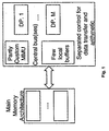
- FIG. 1 A relatively general model (template) abstracting mainly the data transfer and storage architecture for such HW solutions is illustrated in Fig. 1.
- the main memory architecture is separate from the processing capacity (data processors DP) which includes a custom memory management unit (MMU), and some local buffers to control the flow of data between the main processing capacity and the memory.
- the pros and cons of this approach are:
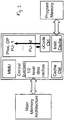
- FIG. 2 A relatively general abstraction of such processors is illustrated in Fig. 2.
- the main memory is accessed via data caches with a separate memory and instruction cache for the program instructions.
- the pros and cons of this approach are:
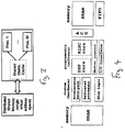
- FIG. 4 The top-level view of a typical heterogeneous system architecture including both custom hardware (accelerator data path, dedicated processor and glue logic) and programmable processors (DSP and RISC cores, master control) in a target application domain is illustrated in Fig. 4.
- Architecture experiments have shown that 50-80% of the area cost in (application-specific) architectures for real-time multi-dimensional signal processing is due to memory units, i.e. single or multi-port RAMs, pointer-addressed memories, and register files.
- the power cost both for custom HW and for SW processors is even more heavily dominated by storage and transfers for complex data types.
- the organization of the global data transfer and storage, together with the related algorithmic transformations form the dominating factors in the system-level architecture design decisions.
- the data transfer and storage architecture for SW processors i.e. the available memory units and the (bus) communication hardware between them together with their use for a given application is power inefficient.
- the present invention includes a programmable processing engine, the processing engine including a customized processor, a flexible processor and a data store commonly sharable between the two processors, the customized processor normally executing a sequence of a plurality of pre-customized routines, comprising: a controller for monitoring the customized processor during execution of a first code portion to flexibly select one of a set of pre-customized processing interruption points in a first routine and for switching context from the customized processor to the flexible processor at the selected interruption point.
- the present invention also includes a method of operating a programmable processing engine, the processing engine including a customized processor, a flexible processor and a data store commonly sharable between the two processors, the customized processor normally executing a sequence of a plurality of pre-customized routines, comprising the steps of: monitoring the customized processor during execution of a first code portion to flexibly select one of a set of precustomised processing interruption points in a first routine; and switching context from the customized processor to the flexible processor at the selected interruption point.
- the method also includes as a next step executing a second code portion on said flexible processor using at least a part of first data left in the data store by the execution of the first code portion on the customized processor.
- the present invention also includes a processor architecture comprising a hierarchy of cache memories, wherein the cache memories are flexibly configurable at run time.
- This processor architecture can be advantageously used in the processing method and apparatus mentioned above.
- the flexibly configurable cache memories may include flexible bypasses over a selectable combination of cache levels of the hierarchy.
- the flexibly configurable cache memories may also include means for allowing signals to reside in a selectable one of the cache levels of the hierarchy for more than one cycle.
- the flexibly configurable cache memories may also include means for allowing different cache levels of the cache memory hierarchy to be merged in a single memory such that the size of each cache level is selectable therefrom.
- the flexibly configurable cache memories may also include means for dividing the cache into banks and means for selectably combining the banks into selectably accessible cache partitions.
- the flexibly configurable cache memories may also include means for allowing selection of the degree of associativity for any cache level.
- the present invention includes architectural and design methodology useful for the inclusion of both custom HW and flexible SW units together on a single-chip system and how to organize the control to allow a considerable flexibility and reprogrammability without increasing power characteristics of the design. This comes as a (much) more cost effective alternative to conventional solutions, where, for instance, fully programmable SW components are applied for the purpose of flexibility.
- the target domain of the present invention includes all real-time data-dominated applications, which deal with large amounts of complex data types. This happens both in real-time multi-dimensional signal processing (RMSP) applications such as video and image processing (which handle indexed array signals, usually in the context of loops), and in sophisticated communication network protocols (which handle large sets of records organized in tables and pointers). Both classes of applications contain many important applications, e.g. video coding, medical image archival, multi-media terminals, artificial vision, xDSL modems, ATM networks, and LAN/WAN technology. Experiments have clearly demonstrated the data-dominated nature of crucial modules in these applications.
- RMSP real-time multi-dimensional signal processing
- SLMM System-level memory management
- Code transformations, memory allocation and cache memory optimization may be advantageously combined with the present invention in order to provide an optimal HW/SW partitioning and HW and/or SW processor memory design, see for example US patents having the serial numbers 08/827,883, “Control flow and memory management and optimisation", and 08/649,903, “Background memory allocation for multi-dimensional signal processing", US 5,742,814, the co-pending European patent application EP 867 808, "Method and apparatus for size optimisation of storage units” and the articles "Code transformations for low power caching on embedded processors", Kulkarni et al., Int. Parallel Proc.
- a processor architecture solution is proposed to obtain more power-efficient flexible processors, e.g. on a programmable processor or a reconfigurable logic circuit.
- the processor architecture impact is very low and involves only the availability of some instructions in the processor instruction set to allow a fine-grain synchronization and data exchange with the custom hardware side.
- reuse of existing processor cores which are modified as little as possible internally, while still obtaining the desired power and speed advantages is an advantage of this embodiment.
- one or more customized processors 21 can be combined with one or more on-chip processor core(s) 22 (instruction set processor, IP), leading to the solution shown schematically in Fig. 6. It assumes that both IP 22 and CP 21 have a selective power-up/down capability.
- This solution can be made reprogrammable at run-time by installing a special interaction protocol between the SW (IP, 22) and HW parts (CP, 21) and by appropriately distributing the tasks over the instruction-set processor(s) (IP, 22) and the custom processor(s) (CP, 21), depending on the given application requirements.
- the processing on HW 2 can switch to SW2 when the relevant data for the new routines on SW2 are available to SW2 via accesses 9 to main memory 23.
- main memory 23 Clearly a trade-off is involved here. If very few points in the algorithm are present where all necessary data is available in main memory 23, the granularity is very coarse and the speed and power overhead of moving the code from HW 21 to SW 22 will be significant because of the large difference in energy-delay product between these 2 solutions. More freedom and a somewhat finer granularity can be provided by adding extra code in the initial part assigned to the CP 21, which makes copies of the relevant data to the main memory 23. But then data transfer and storage overhead is added to the HW side.
- the hardware controller of CP 21 is made more "intelligent" so that it can add these copies only when really needed (i.e. when the access point is needed for a context switch).
- the overhead can be largely avoided.
- the overall efficiency starts dropping but this embodiment will still remain very beneficial as long as a small amount, e.g. not more than about 10%, of the algorithm has to be transferred from CP 21 to IP 22.
- the IP 22 does not necessarily need to be devoted only to the task of backing up the CP 21 when routines have to be moved. It can be multiplexed in time with other normal tasks which are assigned to the SW. Obviously, however, the less time it remains idle from normal tasks, the less freedom there will be to move routines from the CP side. So here also a design trade-off has to be made. If the IP 22 is fully devoted to the CP 21, its overhead in area should be reasonable compared to the CP 21. In that case, the preferred choice is an ASIP (application-specific instruction-set processor) which is dedicated to support the types of routines present in the CP(s) 21 assigned to it.
- ASIP application-specific instruction-set processor
- both CP 21 and IP 22 preferably exhibit effective power-down modes so that they do not consume power unless when performing useful operations. This may include the use of clock gating measures. Also the clock distribution network is preferably separated for the CP 21 and the IP 22. The 2 clocks can be derived from the same master clock for global synchronization, if desired, but this is not crucial.
- the "synchronous islands in an asynchronous sea” concept can be applied where 2 master clocks are present and where the local synchronization between the different synchronous islands is taken care of by handshaking and potentially a small buffer.
- the average rate at which data are communicated is preferably identical at both sides of the asynchronous interfaces to avoid unacceptable buffer overhead.
- This first embodiment is easily extensible to a situation where several CPs 21 are present, each with their own adapted master controller. In that case the IP (which can also be duplicated) has to follow them up concurrently. Obviously, this situation is required if the initial algorithm contains concurrent processes. Especially if they cannot be scheduled statically during the HW mapping, this is unavoidable.
- the dynamically scheduled processes are then preferably moved to different CPs 21, interacting with each other in the conventional way to execute the algorithm, but individually monitored by the IP(s) 22 with the special protocol in accordance with the present invention.
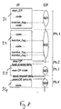
- An example of a protocol to support the above interaction may have 4 phases and may be as follows (see Fig. 8). Assume that one routine 34 or part of a routine has to be moved from the CP 21 to the IP 22 (M3 in Fig. 9). The general case is easily extended from this. Note that the designer has full knowledge and control of what the CP 21 contains and what program is running on the IP 22. This is important in order to allow effective synchronization. The following provides a description of further aspects of this embodiment.
- One important variant of the second embodiment includes the use of a master-master (M-M) interaction between two fully-fledged "stand-alone” controllers where the IP side executes the “overall” control and “pokes” the CP side which then "intelligently” acts based on these events.
- M-M master-master
- the slave instruction based or processor based approaches are usually very acceptable in a context where mainly scalar or control processing has to be performed, as long as the time overhead of the frequent interaction between the CP and IP side is reasonable. That situation is from where the master-slave (M-S) concept originates, but unfortunately the approach breaks down when applied to complex data-dominated routines.
- the designer can switch to the M-S protocol.
- This is shown clearly in the examples of the custom ACU interaction with an ASIP processor for both the M-M (master-master) and M-S (master-slave) embodiments of the present invention detailed below.
- One of the reasons that the M-M protocol may not be preferable is when the cost to do the synchronization in a fine-grain way becomes too large compared to the expected savings.
- a custom ACU with a distributed controller co-operates with an ASIP master controller by adding a special stand-alone controller to the custom ACU.
- the scheduling of the assembly code on the ASIP can be done independently of the (predefined) HW schedule, i.e. the HW can be partly adapted to the ASIP timing.
- This interaction between a custom ACU and an ASIP has been generalized for the flexible co-operation between any IP (with controller + ACUs + ALUs) and a custom ACU in the examples below.
- the experimental results show that the approach works with negligible area/power overhead in the extra controller hardware and that the context switch between CP and IP can be done without real cycle overhead. This allows a very fine grain interaction.
- Data-transfer and storage intensive applications are characterized by a large amount of data-flow (load/store) and control-flow (loops and conditional branches) operations involving background memory (i.e., video-RAM, data-cache). Behind these operations, there is quite a lot of arithmetic (address expressions and conditional tests) related to the computation and the selection of the different pointers needed for the storage. This arithmetic, namely addressing, becomes dominant in the overall arithmetic cost. Typically, the addressing involves many linear and non-linear (e.g., polynomial) arithmetic expressions, as found in leading-edge multimedia and mobile communication applications.
- addressing In addressing, most of the arithmetic is known (manifest) at compile time. Therefore, it can be performed locally, close to the memory address ports. Thus, by using a distributed (custom) addressing architecture in accordance with a further embodiment of the present invention a considerable amount of the routing overhead, typically present in memory dominated architectures, can be avoided.
- this embodiment requires the addressing unit to be physically decoupled from the system processor, for example in a custom Address Calculation Unit (cACU). This partitioning strategy usually leads to better results overall, despite a small overlap in functionality in the control logic. For instance, in accordance with one aspect of this embodiment the occasional duplication of branches which are evaluated by both the system processor and the distributed custom Address Calculation Unit (cACU). Also, the complexity of the system controller is positively affected since most of the control-flow of the addressing, at least the manifest one, is directly managed by the cACU, thus relieving the system processor controller of this task.
- ASIPs Application Specific Instruction-set Processors
- IP Instruction-set Processors
- RISC/DSP cores and multi-media processors Instruction-set Processors
- the following embodiments may provide an efficient fine-grain co-operation between a cACU 31 and a generic IP 32 (Fig. 10).
- the methodology is partly derived from the interaction protocol proposed in the description of the second embodiment of the invention above.
- the use of distributed custom Address Calculation Units (cACUs) 31 in accordance with this embodiment of the present invention allows to meet very tight cycle budgets for both memory-addressing related arithmetic and control-flow with very low area-power overhead. This is especially true for memory intensive applications with quite a lot of complex indexing involved. Still, in most cases, some degree of flexibility is needed to absorb late or after-production specification changes.
- the required flexibility can be achieved by providing a methodology for fine-grain context-switch between the cACU 35 and the programmable instruction-set based processor (IP) 32.
- IP programmable instruction-set based processor
- These embodiments are based on two fine-grain co-operative models for addressing, firstly a concurrent master-master model and secondly a non-concurrent master-slave model.
- This fine-grain context-switch allows to incorporate new functionality with minimal power/cycle overheads, so the saving in moving some addresses from the IP 32 to the cACU 31 is largely kept.
- Decoupling (part of) the addressing functionality from the rest of the system offers the advantage of a fully concurrent (master-master) co-operation model in accordance with this aspect of the first embodiment of the present invention.
- the IP 32 can be devoted to other tasks while the cACU 31 takes care of managing the (distributed) memory 33 itself. Otherwise, if the cACU 31 would just be a "slave", the IP 32 would spend a significant amount of cycles just to control the cACU 31, becoming idle as long as the cACU 31 is busy with the actual computation. Note that it is also possible for the IP 32 to manage some of the memory accesses itself, especially those involving "cheap" addressing, thus leaving the cost-dominant ones to the cACU 31 and enabling a mixed co-operation model.
- a non-concurrent (master-slave) cooperation is possible for cases where only few cACU operations have to be initiated, by explicitly pipelining the cACU operation with other IP-operations some cycles before the address value is needed.
- detailed timing (scheduling) information of the IP-operations will be necessary which is not always available at compile time and which can be avoided by a fully concurrent model.
- the concurrent (master-master) model only the timing information about the actual memory-transfer is mainly needed. It is not necessary then to force the IP scheduler to pipeline operations for explicit synchronization with the cACU 31.
- the order in which the memory-transfers managed by the cACU 31 occur has to be decided beforehand, thus allowing at compile time to know the sequence of events happening in the address bus. Otherwise, the only possible co-operation model is using a master-slave model, where the master IP 32 has to specify the slave cACU 31, (via an encoded instruction) which address expression needs to be provided in the address port, thus putting an extra load on the IP resources. This strategy applies to both master-master and master-slave models.
- a communication channel 34 may be provided for run-time communication of the data-dependencies.
- This channel 34 can be dedicated to this specific purpose.
- DSP and RISC cores one of the available data-busses or dedicated I/O ports can be used. The advantage of using a dedicated channel 34 for the communication is avoiding to overload the existing databus(ses). Thus more freedom is left to the scheduler for the memory-transfers.
- This communication channel 34 is devoted to two purposes:
- All communication between the system processor 32 and the cACU 31 is therefore mainly devoted to resolve only run-time data-dependencies and to explicitly synchronize the evolution of both threads of control (the IP 32 and cACU 31).
- this explicit synchronization is limited to the specific points where the original functionality has to be modified (namely at a context switch), as described above with respect to the second embodiment of the present invention, i.e. a context switch takes place whenever a new functionality is added or modified with respect to the initial version of the application, which means that some parts of the original functionality assigned to the cACU31 are taken over (in a modified form) by the IP 32.
- the IP 32 needs to follow the traversal of the cACU 31, specifically when data-dependent conditional branches are being decided locally in the cACU 31 and the context switch needs to happen inside one or several of them. Normally, the traversed paths result in unbalanced conditional threads. Thus, it becomes very difficult to predict when the context switch should happen. To concurrently match the unbalanced evolution several design options are possible all of which are aspects of this embodiment of the present invention:
- This architecture allows to define a synchronous co-operative model, mainly constrained by the order of the memory accesses that are subject to custom addressing. Otherwise, both performance and cost (area/power) efficiencies can be very limited. Also, the use of related clocks derived from the same system clock 35 is mainly needed for efficiency in the high-level synchronization between both threads of control (the IP 32 and the cACU 31). In the master-master architectures, it affects the synchronization of both schedules (IP 32 and cACU 31). In the master-slave case, it affects the pipelining of the operations of both blocks. In case of related clocks suffering clock-skew problems, it is possible to use a low-level asynchronous protocol for the communication of the data-dependencies, independently of the model chosen.
- a first model allows a master-master concurrent evolution of the two threads of control (one for cACU 31 and one for the IP 32).
- This model is a specific case of the custom block described in a more generic way above in the first embodiment of the present invention and refined for a cACU 31 as an individual embodiment of the present invention.
- the synchronization in this case is implicit by estimating/controlling, but at compile time, the elapsed time between the memory-transfers subject to custom addressing.
- the memory accesses to the slower memories dominate the overall system timing.
- one possibility is to concentrate on the memory-transfer and assume that the compiler will schedule the transfers such that they are kept in the same order as in the original algorithm.
- the second model also allows concurrent co-operation between the two-blocks but now the synchronization is explicit by using a master-slave model where the IP 32 is master of the control-flow.
- the advantage of this model is the simpler design.
- the disadvantage is that the IP 32 is more occupied with controlling the cACU 31 so it cannot perform other tasks while the cACU 31 is busy with the actual address computation or while the interaction to transfer data is going on.
- the operation modes of the first model i.e. a master-master model, will now be described (see Figs. 12A and B) as an embodiment of the present invention.
- the first mode described is the normal operation mode . It is intended for the first functional version of the application, where the cACU 31 is implicitly synchronized with the IP 32 at the points where the memory accesses occur subject to custom addressing.
- the second operation mode ( modified operation mode ) is intended for "modified" versions of the initial functionality.
- explicit synchronization for the points where the context switch takes place are provided.
- the IP 32 has to communicate to the cACU 31 all necessary data-dependencies needed for the address indirection or the conditional branches. These dependencies are stored in a dedicated register file 38 inside the cACU 31 (Fig. 10). The IP 32 "notifies" the cACU 31 that a data-dependency has been transferred by activating a special control line (the data-ready line of Fig. 12 and Fig. 11).
- the cACU 31 starts to compute the next address within the next cycle(s), as soon as the data-dependencies needed for the next address computation are received.
- the cACU 31 "knows" how many data-dependencies need to be communicated at run-time time because the state status of its master controller 37 is known and the number of data-dependencies needed for this particular state is also known at compile time. Thus it is necessary to know at compile time in which exact cycle each of the data-dependencies is going to be communicated.
- the only restriction for this protocol is that the IP 32 must start to communicate all data-dependencies for the actual memory-transfer once the previous memory-transfer has taken place.
- the address expression can be split into subexpressions. Then, each subexpression is computed within one clock cycle and the partial result is stored in a internal register. Therefore, since the cACU 31 also "knows" at compile time how many partial data-dependencies are needed for the actual partial computation, it is always possible to wait until all partial data-dependencies have been transferred and, only then, perform the partial computations progressively.
- the relative order of the communicated data-dependencies should be known at compile time to avoid an overhead in the register file which is devoted to store these dependencies inside the cACU 31.
- this requirement is not essential if the size of the register file 38 can be made large enough.
- the cACU master controller will allocate the received data in the corresponding register 38 whenever the IP 32 "tells" the cACU 31 that a new data value is ready in the communication channel. This is possible since both the IP 32 and the cACU 31 "know” which is the next event (or set of possible events in case of conditional branches) happening on the address bus. Therefore, the assignment of the data of the registers 38 can be decided at compile time.
- the cACU 31 proceeds to provide the address value in the cycle where the IP 32 needs to perform the actual memory-transfer. This can happen without the IP 32 having to know which is the actual bus access protocol of the accessed memory.
- the cACU 31 relieves the IP 32 of the details of the transfer, especially the protocol between the data and the address busses of the memory 42 accessed. This can be extended towards a more genetic customized Memory Management Unit (cMMU) (itself an embodiment of the present invention) that takes care not only of the addressing itself but also of controlling the transfers involved when moving data from one memory hierarchy level to another one (similar to a customized software-controllable cache).
- cMMU Genetic customized Memory Management Unit
- the main pre-requisite to allow full synchronization between the IP 32 and the cACU 31 is to have full control of the evolution of the IP 32 at compile time for timing estimation. Therefore, no run-time interruption nor run-time caching decisions should be allowed at the critical periods of interaction. This can be very easily achieved when using an ASIP as the IP 32, but also other cores like DSPs or even instruction-set based micro-controllers (ARM, etc.) can be used by (temporally) disabling their run-time features.
- the normal operation mode is illustrated in Fig. 11A. Every piece of code between two consecutive memory-transfers (only those decided to be performed in hardware) defines a super-state mode.
- the evolution of the super-states is known by both IP 32 and cACU 31 as explained above.
- the actual memory-transfer triggers the transition between super-states. All necessary data-dependencies are communicated inside each super-state.
- the synchronization with the IP 32 happens implicitly, since the time needed by the IP 32 to compute the code for each super-state is known and controllable at compile-time (T 1, T2, T3, ).
- the IP 32 implicitly avoids scheduling any operation related to the complex address expression in its own ACU 45 since an existing corresponding load/store instruction is used to perform the actual transfer.
- the internal IP ACU (IP-ACU) 45 can be used however to initiate another address computation which is simple enough to remain assigned to the IP 32. Only the cACU 31 needs to disable the access of the IP-ACU 45 to the shared address bus to avoid data collision (see Fig. 12).
- the IP-ACU 45 is again available for the IP controller 44. Note that also between super-states, the IP scheduler 44 is completely free to allocate any operation in its internal ACU 45 for memory accesses which are not initially managed by the cACU 31 (e.g., those which can be very efficiently performed inside the IP-ACU 45).
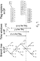
- the procedure to perform the context switch starts whenever the IP 32 "tells" the cACU 31 that a number of memory-transfers should be skipped ( skip-acu (2) in Fig. 11B). Then, the cACU 31 skips the specified number of super-states and goes to a power-down mode.
- the IP 32 synchronizes again with the cACU 31 ( start-acu ) to power-up and continues with the normal operation mode.
- the IP 32 can monitor the evolution of the conditional branches of the cACU 31 by polling the dedicated flag register. To make possible such monitoring without too much overhead, the cACU 31 is preferably able to access the IP register space in the controller 44. Otherwise, the communication of the conditional branch status will have to be done via memory 42 or by introducing a new communication protocol via the existing shared data-bus 46, thus allowing the cACU 31 to dump data on the bus 46 (see also description of first embodiment above).
- a concurrent monitoring of the conditional traversal of the cACU 31 is possible by letting the IP 32 monitor the status (flags) of the conditional branches mapped in the cACU 31, as described with respect to the first embodiment of the present invention above.
- the monitoring of the conditional traversal can be done by letting the IP 32 (at the beginning of the super-state where the context switch should happen) poll a special register 47 where each bit reflects the status of the branch which has been selected (see Fig. 13). To avoid an explosion of the register size, a number of these registers 47 could be used which could be then shared by different portions of the IP code.
- Fig. 13 shows a situation where one of these registers 47 has been allocated.
- the IP 32 can control the time-to-interrupt by using an existing dedicated timer. If the context of the flag register 47 indicates that the branch to be modified is about to be taken, then the cACU 31 is requested to skip the corresponding number of super-states.
- Fig. 13 shows an example of the procedure.
- the interrupt based mechanism can be combined with flag-polling (which doesn't contribute to power degradation) to gradually let the IP 32 monitor the evolution of the cACU 31. Only at the critical points which are close to the context switch, the IP 32 can start the countdown for the moment where the interrupt should happen.
- a master-master protocol it may be beneficial to let the cACU 31 take over all the tasks (including the evaluation of the conditional branches). In this case, then a similar policy for monitoring the status of the cACU 31 as proposed in the first embodiment of the invention could be applied to let the IP monitor the branch selected by the cACU31.
- IP compiler re-schedules the memory transfer operations once it is re-compiled thus changing the order of memory transfers originally present in the code which is situated "after," the context switch (see Fig. 11), at least two alternatives are possible, again depending on the type of IP used (ASIP or DSP/RISC cores).
- the normal operation mode in a full master-slave scheme is intended for a further embodiment of the present invention where the cACU 31 is explicitly synchronized with the IP 32.
- the master-slave scheme is very useful when the synchronization overhead for the master-slave protocol is very low or when the IP 32 cannot do anything useful during these cycles anyway. It is also useful when very little or no control of the IP-scheduler at compile-time is possible (which is the case of some RISC cores).
- both normal and modified operation modes are very similar to the ones proposed for the master-master architecture but now one of the control lines needed from the IP-controller is different ( next-addr in Fig. 15). This line is in charge of performing the explicit synchronization mechanism. This control line is set-up one cycle before the IP controller 44 schedules the actual load/store operation.
- the load/store operation used for the transfer subject to custom addressing should preferably be different than the one used to typically load the address value from the IP-ACU 45. This is required to allow the IP 31 to use its internal ACU 45 for other "cheap" accesses. Many cores have enough instructions available such that an existing load/store operation can be reused.
- the main disadvantage of the master-slave scheme is the impossibility to perform tasks in both IP 32 and cACU 31 concurrently, as is preferred in the first embodiment of the present invention. This results in an extra step necessary to complete the co-operation protocol (see Fig. 15, step 2).
- the cACU 31 must "recognize” when an address needs to be provided ( next-addr ) and this introduces an extra step in the protocol.
- the cACU 31 becomes active and the IP idle until the completion of the address computation (which can usually be done within one clock cycle). This is in contrast to the master-master embodiment where no explicit synchronization is needed. When not too complex or too frequent addresses are provided by the cACU 31 this idle time is acceptable.
- the new instructions can be incorporated easily and the corresponding compiler can be modified without big overhead.
- the instruction-set available is usually large enough to reuse some existing instructions to mimic the desired semantics.
- the next-addr instruction needed for the master-slave model can be mimicked by a simple load/store operation with some control logic that triggers the next-addr as soon as the load/store is being decoded.
- Another example is the ARM architecture which provides two instructions to communicate a data-dependency to a co-processor. These can be reused to execute the operation in the co-processor that could be reused i.e., for the data-ready and the start-acu operations respectively.
- the order in which the data dependency is communicated should be fixed and known at compile time by both cACU and IP schedulers 37, 44.
- the connection between the individual registers 38 of the cACU 31 and the input of the corresponding application-specific arithmetic units, is fixed at compile time (one register for each input).
- the assignment of the data dependency to the individual register 38 is decided at compile time (ordered communication of dependencies) and performed at run-time. Data-dependencies that need to be available during more than one consecutive context switch do not need to be communicated and their value is kept alive in the corresponding register.
- an interface between an ASIP and a cACU 50 is described using the master-slave embodiment (Fig. 16).
- the different addresses expressions have to be extracted from the optimized high level language (e.g. C) specification together with the necessary data-transfers from ASIP to ACU 50. Since the final ordering is not known in this case, the relative ordering of these actions is also extracted from the optimized file, according to the normal procedural execution flow of the code.
- the memory access and data transfer actions correspond respectively to the function calls/control signals from-ato ( ) and to-ato ( ) .
- Fig. 16 gives a global overview of an ACU 50 and its ports.
- the inputs are: CLOCK , addresstick , datatick and databus , the only output is address , which represent: CLOCK : the clock of the ASIP.
- Addresstick this signals the ACU 50 that an address should be calculated. The cycle before the data of a read or write operation has stabilized, this signal should be raised at the positive clock edge. The start of the calculations is triggered by the raising edge of the CLOCK and a high value of addresstick . The address should be calculated in time td (Fig. 17), after which the address bus is decoupled.
- This control signal from the ASIP is associated with the special load/store instruction for the from-ato ( ) function calls.
- Datatick this signals the ACU that valid data is available on the databus 54. This signal should be raised at the positive clock edge, at that moment data is read (Fig. 18). This control signal is associated with the to-ato ( ) function calls.
- Databus the databus 54 is the ASIP datapath. Since the width of the real bus 54 is not known yet, only the relevant width is implemented.
- Address the address bus 55 to which the ACU 50 is connected. Since the final width of the bus 55 is also not known, only the most necessary slice is implemented. The connection is assured by tri-state logic, which is steering the bus while the signal DRIVE is high. This signal becomes high at a positive clock edge when addresstick is high, and goes low at a positive clock edge when addresstick is low (Figs. 17 and 19).
- the first embodiment still has a relatively limited flexibility in the customized points to insert the context switches. This problem can be solved by allowing more impact on the IP architecture.
- the address space of the IP can be extended to also include a subset of the dedicated memories in the CP.
- the programmable processor is allowed to have access (through a shared address space plus a dedicated switch network) to a subset of the dedicated memories inside the custom hardware organization to obtain more power-efficient flexible processor.
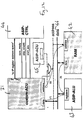
- One detailed organization of an IP 62 and a customized hardware part 61 is shown in Fig. 20 as an example only. Which memories 66 to select is clearly an important design choice.
- the power consumption in the dedicated memory organization 66 of the CP 61 is typically at least an order of magnitude lower than what can be achieved in the very flexible memory pipeline of the IP 62. This requires however more changes in the IP instruction set because also special switches 69 have to be controlled, managing the access between the central IP data busses 65 and the selected CP memories 66.
- a general N x N cross-bar switch is not used here because of the large power overhead involved in that case.
- a power-efficient proposal for this is illustrated in Fig. 22 which is part of the CP 61 so it can be fully tuned.
- One effective solution is to use a multiplexer tree 71, 72 with as many leaves L as there are memory units 66 1 - 66 3 to be accessed in the custom memory hierarchy 66 of the CP 61 and as many roots R as data busses 73, 74 for the IP 62.
- maximally R data have to be provided at the same time so this can be used to simplify the tree further.
- this tree 71, 72 is decoupled from the IP data busses 73, 74 and the CP memory units 66 by switches 69 1 , 69 2 . These should be located as close as possible to the IP data bus and CP memories to enable cost effective decoupling of the switch network capacitance during normal operation.
- switches 69 are selectively powered up only when needed during the interaction protocol.
- address bus rerouting can be organized in a similar way as the examples of the first embodiment (Figs. 12 and 15) given above to be flexible and efficient.
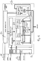
- the architecture allows flexible interaction between the custom ACU 31 and the ACU 45 of the IP as is shown in Figs. 23 and 16.
- the performance of the architecture model of the second embodiment can be summarized as:
- the second embodiment leads to a very power effective solution which is still fully flexible. It also has definite speed advantages compared to the conventional solution where all "flexible" tasks are mapped on the IP. Hence, the energy-delay improvement compared to a full SW solution will be very significant (1 to 2 orders of magnitude if well optimized). The only real physical cost is the extra area which can be kept reasonable. The main bottle-neck therefore is the extra design time which has to be spent and which should be reduced by library and tool support to enable a wide-spread use of this approach.
- the processor core data-path(s) can be used to realize any non data-dominated parts which needs to be flexible, compatible with conventional HW-SW co-design methodologies.
- Central busses and a microcoded controller are used for the arithmetic part just as in the current core-based approaches. Also the fully data-dependent parts (which can only be managed at run-time in terms of data transfer and storage) and the as yet unknown parts at the time of the chip processing have to be still assigned to the SW side.
- run-time hardware control is then responsible for the cache access to the main memories, with a (large) price paid in especially power, even on the state-of-the-art multi-media processors.
- a third embodiment of the present invention will now be described.
- a third embodiment of the present invention more power-efficient fully programmable (parallel) processors are described in which the complete data transfer and storage organization of the programmable processor is modified to be better matched towards the need of a particular multi-media target domain.
- the latter involves much bigger investments in new SW processor design capabilities and advanced compiler technology.
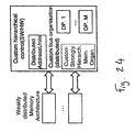
- the proposal is to integrate much more domain-specific customization in the data transfer and storage architecture of multi-media processors, as illustrated in Fig. 24.
- This embodiment of the present invention may be advantageously used with a customized processor.
- the IP architecture shown schematically in Fig. 24 may be advantageously combined with custom processor 21 as shown in Fig. 6 to replace the IP 22.
- Individual aspects of this customization include:
- the implementation of the third embodiment comes partly at the price of reduced flexibility compared to general-purpose RISCs but especially needs a heavy investment in new processor architecture design and compiler technology. The potential savings will be even larger than in the previously described embodiments, however. Recently, some companies have been proposing very domain-specific processors for a limited class of applications. An example is the programmable MIPS MPEG2 engine. These processors still have a limited scope and the data transfer and storage bottle-neck have not been really solved, especially in terms of power.
- the performance of the architecture model of the third embodiment can be summarized as:
- an Inverse Discrete Cosine Transform is preferably expressed as two 1-D IDCT blocks 84, 86 which each process a set of scalar data to combine into one output scalar (Fig. 25).
- IDCT Inverse Discrete Cosine Transform
- the input buffer 82 converts from vertical (V) to horizontal (H) block format and that the output buffer 87 converts from V to H.
- the cost of these buffers is typically quite large and experiments have indicated, for example, that the power consumed by one 1D IDCT data-path and control module is about the same as the transpose buffer 85.
- the saturation arithmetic for the accumulation of the partial row or column results for a particular set of rows or columns can be modified even after the reusable block has been designed and implemented.
- the input and output buffers 82, 87 can be removed by merging them with the transpose buffer 85 by making the appropriate changes in the local code accessing the transpose buffer 85. This may require several context switches between IP 89 and CP 83 but the end result is worth it.
- the addressing of the streams would be integrated in the VHDL code for the 1D IDCT modules 84, 86 and a complete redesign would be required to avoid the buffering.
Landscapes
- Engineering & Computer Science (AREA)
- Theoretical Computer Science (AREA)
- Software Systems (AREA)
- Physics & Mathematics (AREA)
- General Engineering & Computer Science (AREA)
- General Physics & Mathematics (AREA)
- Power Sources (AREA)
- Memory System Of A Hierarchy Structure (AREA)
- Multi Processors (AREA)
Applications Claiming Priority (2)
| Application Number | Priority Date | Filing Date | Title |
|---|---|---|---|
| US6616397P | 1997-11-19 | 1997-11-19 | |
| US66163P | 1997-11-19 |
Publications (2)
| Publication Number | Publication Date |
|---|---|
| EP0918280A1 true EP0918280A1 (de) | 1999-05-26 |
| EP0918280B1 EP0918280B1 (de) | 2004-03-24 |
Family
ID=22067656
Family Applications (1)
| Application Number | Title | Priority Date | Filing Date |
|---|---|---|---|
| EP98121827A Expired - Lifetime EP0918280B1 (de) | 1997-11-19 | 1998-11-17 | System und Verfahren zur Kontextumschaltung über vorbestimmte Unterbrechungspunkte |
Country Status (3)
| Country | Link |
|---|---|
| US (1) | US6223274B1 (de) |
| EP (1) | EP0918280B1 (de) |
| DE (1) | DE69822591T2 (de) |
Families Citing this family (70)
| Publication number | Priority date | Publication date | Assignee | Title |
|---|---|---|---|---|
| JP3573614B2 (ja) * | 1998-03-05 | 2004-10-06 | 株式会社日立製作所 | 画像処理装置及び画像処理システム |
| US8636648B2 (en) | 1999-03-01 | 2014-01-28 | West View Research, Llc | Endoscopic smart probe |
| US10973397B2 (en) | 1999-03-01 | 2021-04-13 | West View Research, Llc | Computerized information collection and processing apparatus |
| US7914442B1 (en) | 1999-03-01 | 2011-03-29 | Gazdzinski Robert F | Endoscopic smart probe and method |
| US8068897B1 (en) | 1999-03-01 | 2011-11-29 | Gazdzinski Robert F | Endoscopic smart probe and method |
| US6446243B1 (en) * | 1999-04-23 | 2002-09-03 | Novas Software, Inc. | Method for functional verification of VLSI circuit designs utilizing reusable functional blocks or intellectual property cores |
| EP1059781B1 (de) * | 1999-05-06 | 2007-09-05 | Siemens Aktiengesellschaft | Kommunikationseinrichtung mit Mitteln zur Echtzeitverarbeitung von zu übertragenden Nutzdaten |
| US7136947B1 (en) * | 1999-06-10 | 2006-11-14 | Cadence Design Systems, Inc. | System and method for automatically synthesizing interfaces between incompatible protocols |
| US6564179B1 (en) * | 1999-07-26 | 2003-05-13 | Agere Systems Inc. | DSP emulating a microcontroller |
| US6408428B1 (en) * | 1999-08-20 | 2002-06-18 | Hewlett-Packard Company | Automated design of processor systems using feedback from internal measurements of candidate systems |
| US6427196B1 (en) * | 1999-08-31 | 2002-07-30 | Intel Corporation | SRAM controller for parallel processor architecture including address and command queue and arbiter |
| US6606704B1 (en) * | 1999-08-31 | 2003-08-12 | Intel Corporation | Parallel multithreaded processor with plural microengines executing multiple threads each microengine having loadable microcode |
| US6668317B1 (en) * | 1999-08-31 | 2003-12-23 | Intel Corporation | Microengine for parallel processor architecture |
| US6983350B1 (en) | 1999-08-31 | 2006-01-03 | Intel Corporation | SDRAM controller for parallel processor architecture |
| US6567975B1 (en) * | 1999-11-08 | 2003-05-20 | Sun Microsystems, Inc. | Method and apparatus for inserting data prefetch operations using data flow analysis |
| US6532509B1 (en) | 1999-12-22 | 2003-03-11 | Intel Corporation | Arbitrating command requests in a parallel multi-threaded processing system |
| US6694380B1 (en) | 1999-12-27 | 2004-02-17 | Intel Corporation | Mapping requests from a processing unit that uses memory-mapped input-output space |
| US6307789B1 (en) * | 1999-12-28 | 2001-10-23 | Intel Corporation | Scratchpad memory |
| US7620702B1 (en) | 1999-12-28 | 2009-11-17 | Intel Corporation | Providing real-time control data for a network processor |
| US6625654B1 (en) * | 1999-12-28 | 2003-09-23 | Intel Corporation | Thread signaling in multi-threaded network processor |
| US6661794B1 (en) | 1999-12-29 | 2003-12-09 | Intel Corporation | Method and apparatus for gigabit packet assignment for multithreaded packet processing |
| US7480706B1 (en) | 1999-12-30 | 2009-01-20 | Intel Corporation | Multi-threaded round-robin receive for fast network port |
| US6584522B1 (en) * | 1999-12-30 | 2003-06-24 | Intel Corporation | Communication between processors |
| US6952824B1 (en) | 1999-12-30 | 2005-10-04 | Intel Corporation | Multi-threaded sequenced receive for fast network port stream of packets |
| US6976095B1 (en) | 1999-12-30 | 2005-12-13 | Intel Corporation | Port blocking technique for maintaining receive packet ordering for a multiple ethernet port switch |
| US6631462B1 (en) * | 2000-01-05 | 2003-10-07 | Intel Corporation | Memory shared between processing threads |
| US6865526B1 (en) * | 2000-01-24 | 2005-03-08 | University Of California-Riverside | Method for core-based system-level power modeling using object-oriented techniques |
| US6732203B2 (en) | 2000-01-31 | 2004-05-04 | Intel Corporation | Selectively multiplexing memory coupling global bus data bits to narrower functional unit coupling local bus |
| US7165257B2 (en) * | 2000-02-08 | 2007-01-16 | Mips Technologies, Inc. | Context selection and activation mechanism for activating one of a group of inactive contexts in a processor core for servicing interrupts |
| US7058065B2 (en) * | 2000-02-08 | 2006-06-06 | Mips Tech Inc | Method and apparatus for preventing undesirable packet download with pending read/write operations in data packet processing |
| US7502876B1 (en) * | 2000-06-23 | 2009-03-10 | Mips Technologies, Inc. | Background memory manager that determines if data structures fits in memory with memory state transactions map |
| US20010052053A1 (en) * | 2000-02-08 | 2001-12-13 | Mario Nemirovsky | Stream processing unit for a multi-streaming processor |
| US7058064B2 (en) * | 2000-02-08 | 2006-06-06 | Mips Technologies, Inc. | Queueing system for processors in packet routing operations |
| US7042887B2 (en) | 2000-02-08 | 2006-05-09 | Mips Technologies, Inc. | Method and apparatus for non-speculative pre-fetch operation in data packet processing |
| US7082552B2 (en) * | 2000-02-08 | 2006-07-25 | Mips Tech Inc | Functional validation of a packet management unit |
| US7155516B2 (en) * | 2000-02-08 | 2006-12-26 | Mips Technologies, Inc. | Method and apparatus for overflowing data packets to a software-controlled memory when they do not fit into a hardware-controlled memory |
| US7649901B2 (en) * | 2000-02-08 | 2010-01-19 | Mips Technologies, Inc. | Method and apparatus for optimizing selection of available contexts for packet processing in multi-stream packet processing |
| US7065096B2 (en) * | 2000-06-23 | 2006-06-20 | Mips Technologies, Inc. | Method for allocating memory space for limited packet head and/or tail growth |
| US7032226B1 (en) | 2000-06-30 | 2006-04-18 | Mips Technologies, Inc. | Methods and apparatus for managing a buffer of events in the background |
| US7076630B2 (en) * | 2000-02-08 | 2006-07-11 | Mips Tech Inc | Method and apparatus for allocating and de-allocating consecutive blocks of memory in background memo management |
| US7139901B2 (en) * | 2000-02-08 | 2006-11-21 | Mips Technologies, Inc. | Extended instruction set for packet processing applications |
| US6622287B1 (en) * | 2000-03-08 | 2003-09-16 | Nec Corporation | Low power hardware/software partitioning approach for core-based embedded systems |
| US7051189B2 (en) * | 2000-03-15 | 2006-05-23 | Arc International | Method and apparatus for processor code optimization using code compression |
| GB0012773D0 (en) * | 2000-05-25 | 2000-07-19 | Radioscape Ltd | Programmable single-chip device and related development environment |
| AU2001278995A1 (en) * | 2000-07-24 | 2002-02-05 | Morphics Technology, Inc. | Distributed micro instruction set processor architecture for high-efficiency signal processing |
| US7236500B1 (en) * | 2000-12-19 | 2007-06-26 | Intel Corporation | Demodulation of multi-user, multi-protocol data in a reconfigurable datapath |
| US6930689B1 (en) * | 2000-12-26 | 2005-08-16 | Texas Instruments Incorporated | Hardware extensions for image and video processing |
| US7165094B2 (en) * | 2001-03-09 | 2007-01-16 | Sonics, Inc. | Communications system and method with non-blocking shared interface |
| JP2002297556A (ja) * | 2001-03-29 | 2002-10-11 | Fujitsu Ltd | マルチプロセッサシステム,マルチプロセッサ制御方法,マルチプロセッサ制御プログラムおよび同プログラムを記録したコンピュータ読取可能な記録媒体 |
| US20040078608A1 (en) * | 2001-04-02 | 2004-04-22 | Ruban Kanapathippillai | Method and apparatus for power reduction in a digital signal processor integrated circuit |
| US7126952B2 (en) * | 2001-09-28 | 2006-10-24 | Intel Corporation | Multiprotocol decapsulation/encapsulation control structure and packet protocol conversion method |
| US7493470B1 (en) * | 2001-12-07 | 2009-02-17 | Arc International, Plc | Processor apparatus and methods optimized for control applications |
| JP2003196333A (ja) * | 2001-12-28 | 2003-07-11 | Nec Electronics Corp | システムlsiの設計方法及びこれを記憶した記録媒体 |
| JP2003263331A (ja) * | 2002-03-07 | 2003-09-19 | Toshiba Corp | マルチプロセッサシステム |
| US8284844B2 (en) | 2002-04-01 | 2012-10-09 | Broadcom Corporation | Video decoding system supporting multiple standards |
| US7471688B2 (en) | 2002-06-18 | 2008-12-30 | Intel Corporation | Scheduling system for transmission of cells to ATM virtual circuits and DSL ports |
| US7017025B1 (en) * | 2002-06-27 | 2006-03-21 | Mips Technologies, Inc. | Mechanism for proxy management of multiprocessor virtual memory |
| US7003630B1 (en) * | 2002-06-27 | 2006-02-21 | Mips Technologies, Inc. | Mechanism for proxy management of multiprocessor storage hierarchies |
| US7352769B2 (en) | 2002-09-12 | 2008-04-01 | Intel Corporation | Multiple calendar schedule reservation structure and method |
| US7433307B2 (en) | 2002-11-05 | 2008-10-07 | Intel Corporation | Flow control in a network environment |
| US7443836B2 (en) | 2003-06-16 | 2008-10-28 | Intel Corporation | Processing a data packet |
| US7370311B1 (en) * | 2004-04-01 | 2008-05-06 | Altera Corporation | Generating components on a programmable device using a high-level language |
| US7409670B1 (en) * | 2004-04-01 | 2008-08-05 | Altera Corporation | Scheduling logic on a programmable device implemented using a high-level language |
| US7395410B2 (en) * | 2004-07-06 | 2008-07-01 | Matsushita Electric Industrial Co., Ltd. | Processor system with an improved instruction decode control unit that controls data transfer between processor and coprocessor |
| US7346863B1 (en) | 2005-09-28 | 2008-03-18 | Altera Corporation | Hardware acceleration of high-level language code sequences on programmable devices |
| US8755515B1 (en) | 2008-09-29 | 2014-06-17 | Wai Wu | Parallel signal processing system and method |
| US8397088B1 (en) | 2009-07-21 | 2013-03-12 | The Research Foundation Of State University Of New York | Apparatus and method for efficient estimation of the energy dissipation of processor based systems |
| JP5485055B2 (ja) * | 2010-07-16 | 2014-05-07 | パナソニック株式会社 | 共有メモリシステム及びその制御方法 |
| US8813018B1 (en) * | 2012-10-05 | 2014-08-19 | Altera Corporation | Method and apparatus for automatically configuring memory size |
| US10621486B2 (en) * | 2016-08-12 | 2020-04-14 | Beijing Deephi Intelligent Technology Co., Ltd. | Method for optimizing an artificial neural network (ANN) |
Citations (4)
| Publication number | Priority date | Publication date | Assignee | Title |
|---|---|---|---|---|
| EP0174231A1 (de) * | 1984-08-02 | 1986-03-12 | Telemecanique | Programmierbare Steuereinrichtung mit Zusatzprozessor |
| EP0442041A2 (de) * | 1990-01-18 | 1991-08-21 | National Semiconductor Corporation | Integrierte, digital arbeitende Signalverarbeitungsanlage/Universalprozessor mit anteilig genutztem internem Speicher |
| EP0794492A2 (de) * | 1996-03-04 | 1997-09-10 | Compaq Computer Corporation | Verteilte Ausführung von modusungeeigneten Befehlen in Multiprozessorsysteme |
| WO1997037300A1 (en) * | 1996-04-02 | 1997-10-09 | Advanced Micro Devices, Inc. | A microprocessor configured to detect an escape instruction indicating a switch between instruction sets |
Family Cites Families (7)
| Publication number | Priority date | Publication date | Assignee | Title |
|---|---|---|---|---|
| US5784611A (en) * | 1994-12-19 | 1998-07-21 | Seagate Technology, Inc. | Device and process for in-system programming electrically erasable and programmable non-volatile memory |
| US6009507A (en) * | 1995-06-14 | 1999-12-28 | Avid Technology, Inc. | System and method for distributing processing among one or more processors |
| JPH10506492A (ja) * | 1995-07-21 | 1998-06-23 | フィリップス エレクトロニクス ネムローゼ フェンノートシャップ | 高性能密度を有するマルチメディアプロセッサアーキテクチャ |
| CN1153129C (zh) * | 1995-09-01 | 2004-06-09 | 菲利浦电子北美公司 | 用于处理器定制操作的设备 |
| US5732275A (en) * | 1996-01-11 | 1998-03-24 | Apple Computer, Inc. | Method and apparatus for managing and automatically updating software programs |
| US6061711A (en) * | 1996-08-19 | 2000-05-09 | Samsung Electronics, Inc. | Efficient context saving and restoring in a multi-tasking computing system environment |
| US5974454A (en) * | 1997-11-14 | 1999-10-26 | Microsoft Corporation | Method and system for installing and updating program module components |
-
1998
- 1998-11-17 DE DE69822591T patent/DE69822591T2/de not_active Expired - Lifetime
- 1998-11-17 EP EP98121827A patent/EP0918280B1/de not_active Expired - Lifetime
- 1998-11-19 US US09/196,645 patent/US6223274B1/en not_active Expired - Fee Related
Patent Citations (4)
| Publication number | Priority date | Publication date | Assignee | Title |
|---|---|---|---|---|
| EP0174231A1 (de) * | 1984-08-02 | 1986-03-12 | Telemecanique | Programmierbare Steuereinrichtung mit Zusatzprozessor |
| EP0442041A2 (de) * | 1990-01-18 | 1991-08-21 | National Semiconductor Corporation | Integrierte, digital arbeitende Signalverarbeitungsanlage/Universalprozessor mit anteilig genutztem internem Speicher |
| EP0794492A2 (de) * | 1996-03-04 | 1997-09-10 | Compaq Computer Corporation | Verteilte Ausführung von modusungeeigneten Befehlen in Multiprozessorsysteme |
| WO1997037300A1 (en) * | 1996-04-02 | 1997-10-09 | Advanced Micro Devices, Inc. | A microprocessor configured to detect an escape instruction indicating a switch between instruction sets |
Also Published As
| Publication number | Publication date |
|---|---|
| DE69822591D1 (de) | 2004-04-29 |
| US6223274B1 (en) | 2001-04-24 |
| EP0918280B1 (de) | 2004-03-24 |
| DE69822591T2 (de) | 2005-03-24 |
Similar Documents
| Publication | Publication Date | Title |
|---|---|---|
| EP0918280B1 (de) | System und Verfahren zur Kontextumschaltung über vorbestimmte Unterbrechungspunkte | |
| US8156284B2 (en) | Data processing method and device | |
| US8914590B2 (en) | Data processing method and device | |
| Faraboschi et al. | The latest word in digital and media processing | |
| Mishra et al. | Tartan: evaluating spatial computation for whole program execution | |
| Benini et al. | System-level power optimization: techniques and tools | |
| US6978389B2 (en) | Variable clocking in an embedded symmetric multiprocessor system | |
| Iyer et al. | Power efficiency of voltage scaling in multiple clock, multiple voltage cores | |
| US7920584B2 (en) | Data processing system | |
| US7836317B2 (en) | Methods and apparatus for power control in a scalable array of processor elements | |
| US7263624B2 (en) | Methods and apparatus for power control in a scalable array of processor elements | |
| Glossner et al. | The sandbridge sb3011 platform | |
| US7302557B1 (en) | Method and apparatus for modulo scheduled loop execution in a processor architecture | |
| Wolf et al. | Memory system optimization of embedded software | |
| Noguera et al. | Dynamic run-time hw/sw scheduling techniques for reconfigurable architectures | |
| WO2004092949A2 (en) | Processing system with instruction-and thread-level parallelism | |
| US20030135778A1 (en) | Data processing system | |
| Gray et al. | Viper: A vliw integer microprocessor | |
| Becker et al. | Scalable processor instruction set extension | |
| JP2003527711A (ja) | データ処理装置、データ処理装置を動作させる方法及びプログラムをコンパイルする方法 | |
| Chen et al. | Flexible heterogeneous multicore architectures for versatile media processing via customized long instruction words | |
| US9003168B1 (en) | Control system for resource selection between or among conjoined-cores | |
| Colnarič et al. | Architectural support for predictability in hard real-time systems | |
| Ernst | Embedded system architectures | |
| Seidel | A Task Level Programmable Processor |
Legal Events
| Date | Code | Title | Description |
|---|---|---|---|
| PUAI | Public reference made under article 153(3) epc to a published international application that has entered the european phase |
Free format text: ORIGINAL CODE: 0009012 |
|
| AK | Designated contracting states |
Kind code of ref document: A1 Designated state(s): BE DE FI FR GB NL SE |
|
| AX | Request for extension of the european patent |
Free format text: AL;LT;LV;MK;RO;SI |
|
| 17P | Request for examination filed |
Effective date: 19990518 |
|
| AKX | Designation fees paid |
Free format text: BE DE FI FR GB NL SE |
|
| GRAH | Despatch of communication of intention to grant a patent |
Free format text: ORIGINAL CODE: EPIDOS IGRA |
|
| RTI1 | Title (correction) |
Free format text: SYSTEM AND METHOD FOR CONTEXT SWITCHING ON PREDETERMINED INTERRUPTION POINTS |
|
| GRAS | Grant fee paid |
Free format text: ORIGINAL CODE: EPIDOSNIGR3 |
|
| GRAA | (expected) grant |
Free format text: ORIGINAL CODE: 0009210 |
|
| AK | Designated contracting states |
Kind code of ref document: B1 Designated state(s): BE DE FI FR GB NL SE |
|
| PG25 | Lapsed in a contracting state [announced via postgrant information from national office to epo] |
Ref country code: NL Free format text: LAPSE BECAUSE OF FAILURE TO SUBMIT A TRANSLATION OF THE DESCRIPTION OR TO PAY THE FEE WITHIN THE PRESCRIBED TIME-LIMIT Effective date: 20040324 Ref country code: FI Free format text: LAPSE BECAUSE OF FAILURE TO SUBMIT A TRANSLATION OF THE DESCRIPTION OR TO PAY THE FEE WITHIN THE PRESCRIBED TIME-LIMIT Effective date: 20040324 |
|
| REG | Reference to a national code |
Ref country code: GB Ref legal event code: FG4D |
|
| REF | Corresponds to: |
Ref document number: 69822591 Country of ref document: DE Date of ref document: 20040429 Kind code of ref document: P |
|
| PG25 | Lapsed in a contracting state [announced via postgrant information from national office to epo] |
Ref country code: SE Free format text: LAPSE BECAUSE OF FAILURE TO SUBMIT A TRANSLATION OF THE DESCRIPTION OR TO PAY THE FEE WITHIN THE PRESCRIBED TIME-LIMIT Effective date: 20040624 |
|
| NLV1 | Nl: lapsed or annulled due to failure to fulfill the requirements of art. 29p and 29m of the patents act | ||
| ET | Fr: translation filed | ||
| PLBE | No opposition filed within time limit |
Free format text: ORIGINAL CODE: 0009261 |
|
| STAA | Information on the status of an ep patent application or granted ep patent |
Free format text: STATUS: NO OPPOSITION FILED WITHIN TIME LIMIT |
|
| 26N | No opposition filed |
Effective date: 20041228 |
|
| PGFP | Annual fee paid to national office [announced via postgrant information from national office to epo] |
Ref country code: BE Payment date: 20051020 Year of fee payment: 8 |
|
| PG25 | Lapsed in a contracting state [announced via postgrant information from national office to epo] |
Ref country code: BE Free format text: LAPSE BECAUSE OF NON-PAYMENT OF DUE FEES Effective date: 20061130 |
|
| BERE | Be: lapsed |
Owner name: *IMEC V.Z.W. Effective date: 20061130 |
|
| PGFP | Annual fee paid to national office [announced via postgrant information from national office to epo] |
Ref country code: DE Payment date: 20091126 Year of fee payment: 12 |
|
| PGFP | Annual fee paid to national office [announced via postgrant information from national office to epo] |
Ref country code: GB Payment date: 20091102 Year of fee payment: 12 Ref country code: FR Payment date: 20091214 Year of fee payment: 12 |
|
| REG | Reference to a national code |
Ref country code: DE Ref legal event code: R081 Ref document number: 69822591 Country of ref document: DE Owner name: IMEC, BE Free format text: FORMER OWNER: IMEC VZW, LEUVEN HEVERLEE, BE Effective date: 20110429 |
|
| GBPC | Gb: european patent ceased through non-payment of renewal fee |
Effective date: 20101117 |
|
| REG | Reference to a national code |
Ref country code: FR Ref legal event code: ST Effective date: 20110801 |
|
| REG | Reference to a national code |
Ref country code: DE Ref legal event code: R119 Ref document number: 69822591 Country of ref document: DE Effective date: 20110601 Ref country code: DE Ref legal event code: R119 Ref document number: 69822591 Country of ref document: DE Effective date: 20110531 |
|
| PG25 | Lapsed in a contracting state [announced via postgrant information from national office to epo] |
Ref country code: FR Free format text: LAPSE BECAUSE OF NON-PAYMENT OF DUE FEES Effective date: 20101130 |
|
| PG25 | Lapsed in a contracting state [announced via postgrant information from national office to epo] |
Ref country code: GB Free format text: LAPSE BECAUSE OF NON-PAYMENT OF DUE FEES Effective date: 20101117 |
|
| PG25 | Lapsed in a contracting state [announced via postgrant information from national office to epo] |
Ref country code: DE Free format text: LAPSE BECAUSE OF NON-PAYMENT OF DUE FEES Effective date: 20110531 |