EP0918449A1 - Schaltung zur Steuerung einer Leuchtstofflampe - Google Patents
Schaltung zur Steuerung einer Leuchtstofflampe Download PDFInfo
- Publication number
- EP0918449A1 EP0918449A1 EP98410130A EP98410130A EP0918449A1 EP 0918449 A1 EP0918449 A1 EP 0918449A1 EP 98410130 A EP98410130 A EP 98410130A EP 98410130 A EP98410130 A EP 98410130A EP 0918449 A1 EP0918449 A1 EP 0918449A1
- Authority
- EP
- European Patent Office
- Prior art keywords
- terminal
- control circuit
- bridge
- lamp
- circuit according
- Prior art date
- Legal status (The legal status is an assumption and is not a legal conclusion. Google has not performed a legal analysis and makes no representation as to the accuracy of the status listed.)
- Granted
Links
- 238000004804 winding Methods 0.000 claims description 65
- 239000003990 capacitor Substances 0.000 claims description 39
- 230000001939 inductive effect Effects 0.000 claims description 23
- 238000005259 measurement Methods 0.000 claims description 7
- 238000010438 heat treatment Methods 0.000 claims description 3
- 238000011084 recovery Methods 0.000 abstract description 2
- 230000037452 priming Effects 0.000 description 7
- 230000007423 decrease Effects 0.000 description 3
- 238000010586 diagram Methods 0.000 description 3
- XEEYBQQBJWHFJM-UHFFFAOYSA-N Iron Chemical compound [Fe] XEEYBQQBJWHFJM-UHFFFAOYSA-N 0.000 description 2
- 238000009825 accumulation Methods 0.000 description 2
- 230000005294 ferromagnetic effect Effects 0.000 description 2
- 230000010363 phase shift Effects 0.000 description 2
- 239000007858 starting material Substances 0.000 description 2
- 239000006096 absorbing agent Substances 0.000 description 1
- 230000015556 catabolic process Effects 0.000 description 1
- 238000006243 chemical reaction Methods 0.000 description 1
- 239000000470 constituent Substances 0.000 description 1
- 238000001816 cooling Methods 0.000 description 1
- 238000006731 degradation reaction Methods 0.000 description 1
- 238000001514 detection method Methods 0.000 description 1
- 230000010354 integration Effects 0.000 description 1
- 229910052742 iron Inorganic materials 0.000 description 1
- 238000002955 isolation Methods 0.000 description 1
- 238000000034 method Methods 0.000 description 1
- 238000012986 modification Methods 0.000 description 1
- 230000004048 modification Effects 0.000 description 1
- 230000021715 photosynthesis, light harvesting Effects 0.000 description 1
- 230000035939 shock Effects 0.000 description 1
- 230000001960 triggered effect Effects 0.000 description 1
Images


Classifications
-
- H—ELECTRICITY
- H02—GENERATION; CONVERSION OR DISTRIBUTION OF ELECTRIC POWER
- H02M—APPARATUS FOR CONVERSION BETWEEN AC AND AC, BETWEEN AC AND DC, OR BETWEEN DC AND DC, AND FOR USE WITH MAINS OR SIMILAR POWER SUPPLY SYSTEMS; CONVERSION OF DC OR AC INPUT POWER INTO SURGE OUTPUT POWER; CONTROL OR REGULATION THEREOF
- H02M5/00—Conversion of AC power input into AC power output, e.g. for change of voltage, for change of frequency, for change of number of phases
- H02M5/02—Conversion of AC power input into AC power output, e.g. for change of voltage, for change of frequency, for change of number of phases without intermediate conversion into DC
- H02M5/04—Conversion of AC power input into AC power output, e.g. for change of voltage, for change of frequency, for change of number of phases without intermediate conversion into DC by static converters
- H02M5/22—Conversion of AC power input into AC power output, e.g. for change of voltage, for change of frequency, for change of number of phases without intermediate conversion into DC by static converters using discharge tubes with control electrode or semiconductor devices with control electrode
- H02M5/275—Conversion of AC power input into AC power output, e.g. for change of voltage, for change of frequency, for change of number of phases without intermediate conversion into DC by static converters using discharge tubes with control electrode or semiconductor devices with control electrode using devices of a triode or transistor type requiring continuous application of a control signal
- H02M5/293—Conversion of AC power input into AC power output, e.g. for change of voltage, for change of frequency, for change of number of phases without intermediate conversion into DC by static converters using discharge tubes with control electrode or semiconductor devices with control electrode using devices of a triode or transistor type requiring continuous application of a control signal using semiconductor devices only
-
- H—ELECTRICITY
- H05—ELECTRIC TECHNIQUES NOT OTHERWISE PROVIDED FOR
- H05B—ELECTRIC HEATING; ELECTRIC LIGHT SOURCES NOT OTHERWISE PROVIDED FOR; CIRCUIT ARRANGEMENTS FOR ELECTRIC LIGHT SOURCES, IN GENERAL
- H05B41/00—Circuit arrangements or apparatus for igniting or operating discharge lamps
- H05B41/14—Circuit arrangements
- H05B41/16—Circuit arrangements in which the lamp is fed by DC or by low-frequency AC, e.g. by 50 cycles/sec AC, or with network frequencies
- H05B41/18—Circuit arrangements in which the lamp is fed by DC or by low-frequency AC, e.g. by 50 cycles/sec AC, or with network frequencies having a starting switch
-
- H—ELECTRICITY
- H05—ELECTRIC TECHNIQUES NOT OTHERWISE PROVIDED FOR
- H05B—ELECTRIC HEATING; ELECTRIC LIGHT SOURCES NOT OTHERWISE PROVIDED FOR; CIRCUIT ARRANGEMENTS FOR ELECTRIC LIGHT SOURCES, IN GENERAL
- H05B41/00—Circuit arrangements or apparatus for igniting or operating discharge lamps
- H05B41/14—Circuit arrangements
- H05B41/36—Controlling
- H05B41/38—Controlling the intensity of light
- H05B41/39—Controlling the intensity of light continuously
- H05B41/392—Controlling the intensity of light continuously using semiconductor devices, e.g. thyristor
- H05B41/3921—Controlling the intensity of light continuously using semiconductor devices, e.g. thyristor with possibility of light intensity variations
- H05B41/3924—Controlling the intensity of light continuously using semiconductor devices, e.g. thyristor with possibility of light intensity variations by phase control, e.g. using a triac
-
- Y—GENERAL TAGGING OF NEW TECHNOLOGICAL DEVELOPMENTS; GENERAL TAGGING OF CROSS-SECTIONAL TECHNOLOGIES SPANNING OVER SEVERAL SECTIONS OF THE IPC; TECHNICAL SUBJECTS COVERED BY FORMER USPC CROSS-REFERENCE ART COLLECTIONS [XRACs] AND DIGESTS
- Y10—TECHNICAL SUBJECTS COVERED BY FORMER USPC
- Y10S—TECHNICAL SUBJECTS COVERED BY FORMER USPC CROSS-REFERENCE ART COLLECTIONS [XRACs] AND DIGESTS
- Y10S315/00—Electric lamp and discharge devices: systems
- Y10S315/05—Starting and operating circuit for fluorescent lamp
Definitions
- the present invention relates to the field of lamps fluorescent lamps supplied from the high-voltage AC network (for example, 220 volts / 50 Hz).
- the invention relates more particularly the lamp control, essentially, by current limitation in nominal operation and in ignition.
- starter an element priming or starting, generally called “starter”, intended to heat the filaments contained in the fluorescent lamp first, then start it with a surge.
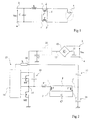
- Figure 1 shows an example of a classic diagram power supply of a fluorescent lamp.
- a lamp 1 is generally consisting of a tubular element T filled with gas and at the two ends of which are provided two filaments f, f ' of excitement.
- Each filament is intended to be electrically connected by its two ends and is therefore associated with two terminals 1, 2, respectively 1 ', 2', supply.
- Both filaments f, f ' are intended to be supplied by a voltage alternative Vac, for example, the applied line voltage between two terminals 3, 4 for supplying the lamp circuit.
- the element of current limitation consists of an inductance L in iron, of high value, inserted between a first supply terminal 3 alternative and a first terminal 1 of one of the filaments f of the lamp T.
- the second terminal of the filament f is connected, by via a starting element 5, at a terminal 2 'of the second filament f ', the other terminal 1' of which is connected to the second power supply terminal 4 in the sector.
- a capacitor C connects terminals 3 and 4.
- the starting or starting element 5 is, most often consisting of a thermal switch intended to heat the filaments f and f 'of the lamp T by short-circuiting the terminals 2 and 2 'as long as the filaments are cold.
- the switch thermal opens as soon as it reaches a given temperature, this which causes an overvoltage triggering the ignition of the lamp thanks to the energy reserve constituted by the inductor L.
- the role of the inductor L is, in nominal operation, to limit the current in the lamp T so that its voltage does not exceed the value for which it is designed.
- the role of capacitor C is to compensate for the phase shift linked to mounting inductive in order to improve the power factor and the make it acceptable for connection to the network.
- a disadvantage of a conventional feeding system as shown in Figure 1 is that the use of strong inductance (usually around 1 Henry) leads to a system bulky and heavy.
- the inductive nature of the assembly which requires compensation for the phase shift by the capacitor C requires a large capacitor (usually more than 10 ⁇ F), therefore electrolytic.
- Another disadvantage of such a system is that it there is no suitable light intensity dimmer.
- Figure 2 shows an example of a classic diagram limiting circuit called "electronic", that is to say putting using active components to limit the current of the fluorescent lamp in nominal operation.
- Such a circuit consists of a bridge 10 of diodes of which two terminals for applying an alternating voltage are connected to two terminals 3, 4 for applying the Vac voltage of the sector.
- a first rectified output terminal 11 of bridge 10 constitutes a ground terminal of the circuit.
- a second terminal 12 of rectified output of bridge 10 delivers, using a capacitor electrolytic C 'of high value, a continuous supply at a switching converter 13 used to power the fluorescent lamp T.
- the switching converter 13 is generally consisting of a control circuit 14 associated with two transistors Power MOS M1, M2 (or two bipolar transistors) connected in series between terminal 12 of bridge 10 and earth, the capacitor Being connected in parallel to this association in series.
- a terminal 15 of the switching converter is connected to a first terminal of a high frequency inductor L 'rise, as in the case of FIG. 1, in series with one of the filaments f of lamp T.
- a capacitor C "of low value connects the filaments f and f ', and participates in the ignition of the lamp.
- the second terminal 1 'of the filament f' is connected to ground by through a capacitor 16.
- Another capacitor 17 connects terminal 1 'to an input terminal 18 of the converter cutting 13.
- the capacitors 16 and 17 are used to filter the DC component in the T lamp.
- Terminal 18 receives the voltage continuous delivered by the capacitor C '.
- the transistor M1 is connected between terminal 18 and terminal 15 and transistor M2 is connected between terminal 15 and earth.
- Transistors M1 and M2 are controlled by circuit 14 which also includes a reaction input connected to terminal 15 and which is supplied to from terminal 18 via a resistor R.
- a capacitor 19 connects terminals 15 and 18 and participates in generation an auxiliary power supply necessary for controlling the transistor M1.
- Circuit 14 may include other configuration terminals and parameters not shown.
- the functioning an electronic limitation circuit as shown in Figure 2 is perfectly known.
- Bridge 10 and capacitor C ' provide, for an alternating voltage of 220 volts, a power supply of the order of 300 DC volts to the converter at cutting which is of the "symmetrical half-bridge" type.
- This converter supplies alternating current at a frequency generally approximately 30 kHz to the fluorescent lamp T via high frequency inductance (in series) L 'which can be low value (of the order of mH).
- a system as shown in Figure 2 saves the use of a high inductance (L, Figure 1).
- a drawback of a circuit as shown in Figure 2 is that it still requires a capacitor high value electrolytic C '(generally greater than 10 ⁇ F) to filter the voltage rectified by bridge 10. Recourse to electrolytic capacitors harms the life of the circuit.
- Another drawback of the system shown in the figure 2 is that it requires two high power MOS transistors voltage that operate at high frequency.
- the present invention aims to overcome the drawbacks known systems for supplying fluorescent lamps.
- the invention aims, in particular, to propose a new control circuit of a fluorescent lamp which provides a limitation nominal current while being compact and at least partially integrable.
- the present invention also aims to provide a solution which allows to add an intensity gradation function luminous to the control system.
- the present invention also aims to improve the reliability of the control system by avoiding the use of electrolytic capacitors.
- a feature of the present invention is provide a fluorescent lamp power supply sine wave at low frequency corresponding to the mains frequency (for example, 50 hertz) while avoiding the use of an inductor of high value by means of an active circuit operating at a higher frequency (for example, of the order of 100 kHz).
- a device is used active to power the fluorescent lamp by controlling its current.
- This device provides low alternating current frequency with fluorescent lamp of a shape similar to that a ferromagnetic type limiting circuit, i.e. using a simple high value inductor.
- the present invention provides a control circuit for a fluorescent lamp comprising means for supplying low frequency alternating current to the fluorescent lamp, these means being controlled by a source of switching current, controllable and operating at frequency high.
- the circuit includes a voltage rectifier bridge low frequency AC power supply and between two terminals rectified output of the bridge, at least one constituent switch of the switching current source.
- An inductive element being controlled by the switch.
- control circuit includes means for recovering energy said inductive element (s) when the switch is open.
- the switch is connected in series with a measuring resistor between two rectified output terminals of the rectifier bridge, the switch being controlled by a circuit from a measurement of the current in the resistor.
- the switching current source is supplied between the two bridge rectified output terminals.
- the lamp is connected between a first terminal of the power supply low frequency AC and a first AC input terminal from the bridge to which the other alternative input terminal is connected to a second terminal of the AC power supply.
- a low value capacitor is connected in parallel with a serial association of a low value inductor and the lamp.
- only one inductive element is connected in series with the switch between the bridge rectified output terminals.
- the bridge has, between its first alternative input terminal and each of the rectified output terminals, an inductive element.
- said means comprise an inverter controlled at the frequency of the AC supply voltage and suitable for operating freewheeling an inductive element during opening periods of the switch.
- the bridge has a first inductive element in series with a first diode of the bridge between said second terminal of the power supply AC and a first rectified output terminal, and a second inductive element in series with a second diode between said first alternative input terminal and said first rectified output terminal.
- said first inductive elements constitute windings respective primary of two isolation transformers of the lamp in relation to the AC supply voltage.
- each transformer has a first secondary winding heating a filament of the lamp.
- each transformer further comprises a second winding secondary intended to start the lamp while forming, with a condenser connected between first terminals of the filaments, a circuit charge pump.
- each transformer has a third secondary winding intended to power the lamp once started.
- control circuit includes means for varying the light intensity of the fluorescent lamp.
- FIG. 3 represents a first embodiment a supply circuit for a fluorescent lamp T according to the present invention.
- Such a circuit consists of a bridge 10 of diodes D1, D2, D3, D4, providing on two output terminals 12, 11, one rectified alternating voltage.
- a first power supply terminal bridge alternative is connected to a first application terminal 3 an alternating supply voltage, for example the mains voltage Vac.
- a second terminal 30 of alternative power supply bridge 10 is connected to a second terminal 4 of the power supply of the sector, at least via the T lamp.
- a feature of the present invention according to this embodiment which basically distinguishes it a conventional control circuit as shown in the figure 2, is that the lamp T is connected to alternating voltage terminals from the bridge and not to rectified voltage terminals.
- limiting the current in the lamp is effected by a switching current source associated with a current measurement resistance Rs.
- This source of current consists essentially of a switch 31 (for example a MOS transistor, a bipolar transistor, etc.) connected in series with the resistor Rs between terminals 12 and 11 of rectified output of bridge 10.
- Switch 31 is controlled by an electronic circuit 32 from the voltage Vr measured at resistor Rs terminals. Circuit 32 is supplied between the terminals 12 and 11.
- an inductive element 33 here the primary winding of a transformer 39, is inserted in series between terminal 12 and switch 31.
- an inductor L ' is inserted in series between the terminal 30 and the first filament f of the lamp T.
- this inductance L ' is of low value (for example, of from 1 to 10 mH) because its role is not, unlike a circuit as shown in Figure 1, to limit the current in the lamp T, but to constitute a brake at the current peak linked to the presence of a capacitor C1 between terminals 30 and 4.
- the winding 33 of the transformer is used to store energy and to slow down the slope of the current in the resistance Rs at each closing the switch 31.
- one of the secondary windings 34, 35 is used to recover reactive energy to limit energy dissipation.
- the switch 31 is opened, the stored energy in winding 33 is returned to capacitor C1 by a secondary windings 34, 35 of the transformer according to the alternation considered.
- a first secondary winding 34 is connected at series with a diode D6 between terminal 30 and a first terminal 36 of an inverter 37 whose second terminal 38 is connected in series with a second secondary winding 35 and a diode D7 at the same terminal 30.
- the common point of the inverter 37 is connected to terminal 4 and diodes D6 and D7 are mounted in opposite directions one in relation to the other.
- the inverter 37 is controlled by the frequency of the AC power supply Vac and alternately switches from a position where it connects terminal 30 to terminal 4 by through diode D7 and winding 35 and a position where it connects terminal 4 to terminal 30 via winding 34 and diode D6.
- circuit 32 is designed so that the frequency of the switch closing cycles 31 is very much higher than the frequency of feeding alternative.
- circuit 32 is designed so that switch 31 is closed at a frequency of 100 kHz, sound opening being triggered at each cutting period, by a measurement of the current flowing in the resistor Rs.
- the capacitor C1 may be of low value (for example, of the order of a hundred nanofarads).
- the lamp fluorescent T is associated with a conventional starting element 5.
- the system described above makes it possible to generate a low frequency alternating current which is suitable for power supply of a fluorescent lamp.
- the two secondary windings 34 and 35 of transformer 39 must be the same size with respect to to each other and be adapted to the nominal lamp voltage fluorescent. However, it is not necessary that the size secondary windings 34 and 35 correspond to half the size of the primary winding 33. For example, assuming a primary winding of 220 turns and a lamp designed to have nominal operation at 90 volts, the windings secondary 34 and 35 comprise of the order of 90 turns each.
- Figure 4 shows a second embodiment a control circuit for a fluorescent lamp T according to the present invention.
- This embodiment differs from that shown in the Figure 3 by the fact that the energy recovery function reactive when the cutting switch is opened (here, symbolized by a MOS transistor M) is met, no longer by a transformer, but by inductors 40, 41.
- two inductors 40 and 41 are respectively connected in series with a diode D4, D3 of the rectification bridge 10 '.
- Dots respective medium of the series associations of the diodes, respectively D3, D4, and inductors, respectively 41, 40, are connected to the respective terminals 36, 38 of the inverter 37 via diodes, respectively D6, D7.
- a circuit 32 of switch M control measures the voltage Vr aux terminals of a resistor Rs connected in series with the switch M between terminals 12 and 11 of bridge 10 '. The rest of the circuit is not modified compared to the assembly exposed in relation to the figure 3.
- the current flows, when the switch M is closed, in the diode D1, in the transistor M, in resistor Rs, in diode D3 and in inductor 41 to charge capacitor C1.
- the current then flows in free wheel through inductance 41 and the diode D6, the inverter 37 being closed on the contact 36 for positive alternations.
- the same reasoning applies during negative half-waves, through inductance 40, the diode D4, transistor M, resistance Rs, diode D2 during the switch-off and wheel-release periods at through inductor 40 and diode D7 when the switch is open, the reverser 37 being closed on the contact 38 during the negative alternations.
- the choice of the first or second embodiment depends, for example, on the number of inductive elements desired in the circuit and / or the availability of a high transformer frequency (Figure 3).
- FIGS. 5A to 5D respectively represent the shapes of the voltage V T and of the current I T of the fluorescent lamp. It is assumed that the lamp is in nominal operation, that is to say that the ignition element 5 is open.
- FIGS. 5C and 5D respectively illustrate the closing periods of the switch 31 and the current Is in the measurement resistor Rs. In FIG. 5C, the closing periods of the switch 31 have been symbolized by states 1 and the opening periods by states 0.
- the switch 31 is controlled at a high frequency, for example of the order of 100 kHz and the current Is has the form of a train of teeth saw whose amplitude is fixed by the predetermined, known threshold of circuit 32.
- the role of shock absorber of current in resistance Rs played by the inductive element (33, figure 3 - 40 or 41, figure 4) in series with the switch, which slows the slope of the current when the switch 31 closes or M.
- the voltage V T (FIG. 5A) is limited to a value VO which depends on the power of the fluorescent lamp. For example, for a fluorescent lamp with a power of 20 watts, which leads to a nominal operating voltage of the order of 50 effective volts, the control circuit 32 is then dimensioned to deliver an average current of the order of 400 milliampere rms over a period of the supply voltage Vac.
- the current I T in the lamp T is at the frequency of the alternating supply Vac by being smoothed by the inductance L '.
- the delay ⁇ t present at each start of alternation corresponds to the time taken by the voltage Vac to reach the ignition voltage of the lamp (for example, its limitation voltage VO).
- circuit 32 is designed to modulate the current drawn from the sector, for example, according to a sinusoid in phase with the line voltage. Such modulation makes it possible in particular to improve the power factor and / or get a gradation of the light intensity as we will see later.
- FIG. 6 represents an embodiment of a inverter 37 controlled at the frequency of the AC supply of the sector.
- inverter 37 controlled at the frequency of the AC supply of the sector.
- other structures suitable reversers may be used.
- the inverter here consists of two thyristors Th1, Th2, cathode trigger and anode trigger respectively, associated in series with the secondary windings 34 and 35.
- the cathode of thyristor Th1 is connected to terminal 30 of the bridge (10, figure 3) and its anode is connected to a first end of the secondary winding 34 including a second end is connected to terminal 4 via diode D6.
- the anode of thyristor Th2 is connected to terminal 30 and its cathode is connected to terminal 4 through the association in series of winding 35 and diode D7.
- the respective triggers of cathode and anode of thyristors Th1 and Th2 are connected, each via a resistor R, to the AC terminal 3.
- the resistances R are of high value (for example, on the order of several hundred K ⁇ ) to limit the current in the triggers of the thyristors Th1 and Th2.
- thyristor Th1 turns on as soon as its trigger current is sufficient to start it, while the thyristor Th2 which is trigger anode cannot be passed due to the direction of its current trigger. Conversely, during negative alternations, thyristor Th1 remains blocked while thyristor Th2 is turned on.
- inverter 37 at the frequency of the voltage alternative feeding can be done by others means as those illustrated by way of example in FIG. 6.
- An advantage of the present invention is that it allows replace a ferromagnetic type limitation circuit (Figure 1) heavy and bulky by an active electronic circuit small footprint in which all components can be integrated. Indeed, the respective values of the elements inductive and capacitive are perfectly suited to such a integration. In particular, the inductive elements have values of the order of mH.
- the capacitor C1 is, according to the present invention, a capacitor with a value of the order of one hundred nanofarads. Lack of use of an electrolytic capacitor considerably improves the service life of the control system.
- Another advantage of the present invention is that it requires only one power transistor operating at high frequency.
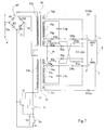
- FIG. 7 shows a third embodiment a control circuit for a fluorescent lamp according to the present invention.
- the embodiment illustrated in FIG. 7 is particularly suitable for a control circuit in which a power dimming is carried out and is intended to replace, not only the classic current limiter (ballast), but also the starter element.
- ballast classic current limiter
- This circuit also provides a current source at cutting 31, 32 controllable and operating at high frequency.
- This current source is, as in the embodiments previous, for example consisting of a switch 31 mounted in series with a resistance Rs for measuring the current between terminals 12 and 11 of rectified output of a 10 "diode bridge.
- the switch 31 is, as before, controlled by a circuit electronic 32 from the voltage Vr measured at the terminals resistance Rs.
- the 10 "righting bridge includes, in two of its branches, a primary winding of a transformer associated with the half-waves concerned by the branch. So the anode of diode D1 of the 10 "bridge is connected to the voltage application terminal 3 Vac alternative, while the cathode of diode D1 is connected to a first terminal of a 33p winding of a first transformer 50, the second terminal of which constitutes the output terminal 12 positive of the rectified power supply.
- the anode of the diode D4 is connected to the second AC supply terminal 30 from the 10 "bridge (connected to the second terminal 4 of the power supply sector), the cathode of diode D4 being connected to a first terminal of a primary winding 33n of a second transformer 51 associated with negative alternations and whose second terminal is connected to terminal 12.
- the rest of the bridge (diodes D2, D3) is similar to a conventional diode bridge such as as shown in Figure 3.
- each secondary of transformers 50 and 51 includes three windings, respectively 52p, 53p, 54p, and 52n, 53n, 54n.
- the windings 53p and 54p (respectively 53n and 54n) have a point common 55p (55n).
- Winding 52p (52n) has nothing in common with the other secondary windings.
- the windings 54p and 54n have one thing in common 56.
- the structure of the circuits, secondary side of the transformers, is similar for each transformer respectively associated with positive or negative alternations.
- the components intervening during positive alternations are identified by the letter p.
- Identical components involved in alternation negative have the same reference associated with the letter not.
- the circuit shown in Figure 7 allows priming of the T lamp thanks to a charge pump type operation using windings 53 and 54.
- This circuit corresponds, for each transformer 50 and 51, to a converter called "with accumulation isolated "(flyback).
- the midpoint 55p (55n) of the windings 53p and 54p (53n and 54n) is connected, via two diodes D8p, D9p (D8n, D9n) in series, to a first terminal 1 (1 ') of a filament f (f ') of lamp T.
- Terminal 1 (1') is connected by via winding 52p (52n) mounted in series with a diode D10p (D10n), at the second terminal 2 (2 ') of the filament concerned f (f ').
- An accumulation capacitor C2 is connected between terminals 1 and 1 '. Note that this capacitor is, according to the invention, with a value of the order of a few tens nanofarads and therefore does not need to be electrolytic.
- the winding terminal 53p (53n), opposite point 55p (55n), is connected to the midpoint of the serial association of the diodes D8p and D9p (D8n and D9n) via a C3p capacitor (C3n) of low value (of the order of a hundred picofarads).
- the circuit associated with the secondary of one of the transformers is closed via a thyristor, respectively Thp or Thn, connected between the terminal of capacitor C2 which is opposite to the terminal of filament 1 (1 ') concerned with the alternation, and the midpoint 56 between the windings 54p and 54n.
- the anode of thyristor Thn is connected to terminal 1.
- the anode of thyristor Thp is connected to terminal 1 '.
- the respective cathodes of thyristors Thn and Thp are connected to point 56.
- each thyristor is also connected to the point 56 by means of a resistor R2p, R2n constituting, with the resistance R1p, R1n concerned, a divider bridge resistive between point 56 and terminal 1, respectively 1 ', of the T lamp.
- the thyristor Thp is conductive, while the thyristor Thn is blocked. Note that the pump pump capacitor C2 charge accumulates energy and sees the voltage across its terminals increase as well during the positive alternations as during negative alternations.
- the voltages of the secondary windings of transformers are a function of respective turns of these windings.
- winding 53p is of higher tension than winding 54p, and that winding 52p is the tension winding the weaker.
- the winding 54p is made with a wire of sufficient section, insofar as this winding must be designed to pass the nominal current lamp T once started.
- the preheating winding 52p of the filament f is of a tension 8 to 10 volts until the lamp is started. This tension drops to 4 volts once the lamp has started.
- the winding 54p has a voltage of a few hundred volts.
- the winding 53p has the highest tension of the secondary windings, for example, around 500 to 1000 volts, as long as the lamp is not not primed.
- An advantage of the embodiment illustrated in relation with figure 7 is that it lends itself particularly to a function dimming. Indeed, thanks to the presence of the filament preheating 52p, 52n windings f and f ', we avoid any flickering of the lamp T by its cooling in the event of a drop in light intensity, therefore drop in power transmitted to transformer secondary. With a classic priming circuit that works according to a thermal principle, the priming circuit causes cuts untimely and random lamp.
- transformers 50 and 51 which have been shown in Figure 7 with a common point 12 of the windings primaries 33p and 33n are particularly suitable for realization of the circuit of the invention by means of a transformer integrable.
- Point 12 becomes again then the anodes of diodes D1 and D4, as in the previous figures.
- the operation of the circuit is not however modified compared to that exposed in relation to Figure 7.
- the embodiment illustrated by the Figure 7 has the same advantages as the embodiments precedents with regard to the lack of recourse to a strong inductance and the absence of recourse to an electrolytic capacitor.
- the circuit of Figure 7 corresponds to a complete electronic "ballast" (priming, preheating, possibility degradation).
- this circuit is particularly applicable well in case we want the lamp T to be isolated from sector.
- the present invention is capable of various variants and modifications which will appear to the man of art.
- the respective dimensions of the different components used will be adapted according to the power fluorescent lamp.
- the arrangements described above as an example can be modified provided that they respect the functional characteristic of creating a current source at high frequency chopping while providing current low frequency alternative to fluorescent lamp.
Landscapes
- Engineering & Computer Science (AREA)
- Power Engineering (AREA)
- Circuit Arrangements For Discharge Lamps (AREA)
Applications Claiming Priority (4)
| Application Number | Priority Date | Filing Date | Title |
|---|---|---|---|
| FR9714869 | 1997-11-21 | ||
| FR9714869A FR2771589A1 (fr) | 1997-11-21 | 1997-11-21 | Limiteur de courant pour lampe fluorescente |
| FR9801246 | 1998-01-29 | ||
| FR9801246A FR2771590B1 (fr) | 1997-11-21 | 1998-01-29 | Circuit de commande de lampe fluorescente |
Publications (2)
| Publication Number | Publication Date |
|---|---|
| EP0918449A1 true EP0918449A1 (de) | 1999-05-26 |
| EP0918449B1 EP0918449B1 (de) | 2006-07-26 |
Family
ID=26233953
Family Applications (1)
| Application Number | Title | Priority Date | Filing Date |
|---|---|---|---|
| EP98410130A Expired - Lifetime EP0918449B1 (de) | 1997-11-21 | 1998-11-20 | Schaltung zur Steuerung einer Leuchtstofflampe |
Country Status (4)
| Country | Link |
|---|---|
| US (1) | US6222325B1 (de) |
| EP (1) | EP0918449B1 (de) |
| DE (1) | DE69835328T2 (de) |
| FR (1) | FR2771590B1 (de) |
Families Citing this family (13)
| Publication number | Priority date | Publication date | Assignee | Title |
|---|---|---|---|---|
| US6538395B2 (en) * | 1999-10-15 | 2003-03-25 | 1263357 Ontario Inc. | Apparatus for dimming a fluorescent lamp with a magnetic ballast |
| JP2002289385A (ja) * | 2001-03-23 | 2002-10-04 | Harison Toshiba Lighting Corp | 放電灯駆動装置 |
| US6400098B1 (en) | 2001-08-21 | 2002-06-04 | Sonlex Limited | Compact fluorescent lamp dimmers |
| KR100915850B1 (ko) * | 2001-11-30 | 2009-09-07 | 코닌클리케 필립스 일렉트로닉스 엔.브이. | Hid 램프를 구동시키는 방법 및 장치 |
| WO2003079739A1 (de) * | 2002-03-20 | 2003-09-25 | Gernot Hass | Scheinwerfersystem mit regeleinrichtung |
| US6727665B2 (en) * | 2002-05-30 | 2004-04-27 | Star Bright Technology Limited | Dimmer for energy saving lamp |
| US7277106B2 (en) * | 2002-07-10 | 2007-10-02 | Samsung Electronics Co., Ltd. | Scanning apparatus having a fluorescent lamp and control method thereof |
| US7560866B2 (en) * | 2005-04-18 | 2009-07-14 | Marvell World Trade Ltd. | Control system for fluorescent light fixture |
| US7414369B2 (en) * | 2005-04-18 | 2008-08-19 | Marvell World Trade Ltd. | Control system for fluorescent light fixture |
| US7619447B2 (en) * | 2005-09-27 | 2009-11-17 | Marvell World Trade Ltd. | High voltage high side transistor driver |
| EP2138017B1 (de) * | 2007-04-23 | 2011-06-15 | Osram Gesellschaft mit beschränkter Haftung | Schaltanordnung zum betreiben einer niederdruck-gasentladungslampe |
| US8138676B2 (en) * | 2008-12-01 | 2012-03-20 | Mills Robert L | Methods and systems for dimmable fluorescent lighting using multiple frequencies |
| CN107979890A (zh) * | 2017-11-29 | 2018-05-01 | 扬州亿芯微电子有限公司 | 一种用于led路灯的带功率因数校正的驱动电路 |
Citations (9)
| Publication number | Priority date | Publication date | Assignee | Title |
|---|---|---|---|---|
| FR2168436A1 (de) * | 1972-01-19 | 1973-08-31 | Philips Nv | |
| EP0021508A1 (de) * | 1979-06-15 | 1981-01-07 | Philips Patentverwaltung GmbH | Schaltungsanordnung zum Zünden und Betrieb einer Gas- und/oder Dampfentladungslampe |
| GB2067318A (en) * | 1979-12-04 | 1981-07-22 | Zumtobel Ag | Circuit arrangement for regulating the power drawn by at least one load from a supply network |
| US4302717A (en) * | 1980-02-04 | 1981-11-24 | Fairchild Camera And Instrument Corp. | Power supply with increased dynamic range |
| US4970437A (en) * | 1989-07-10 | 1990-11-13 | Motorola Lighting, Inc. | Chopper for conventional ballast system |
| WO1992003898A1 (en) * | 1990-08-17 | 1992-03-05 | Gaslamp Power And Light | System for providing a constant level current to a fluorescent tube |
| DE4200900A1 (de) * | 1991-03-15 | 1992-09-17 | Philips Patentverwaltung | Schalteinrichtung |
| EP0633711A1 (de) * | 1992-03-25 | 1995-01-11 | Toto Ltd. | Leistungsregler für eine entladungslampe und beleuchtungsapparat mit variabler farbe, versehen mit solch einem leistungsregler |
| WO1995012157A1 (en) * | 1993-10-27 | 1995-05-04 | Lighting Control, Inc. | Switchmode ac power controller |
Family Cites Families (11)
| Publication number | Priority date | Publication date | Assignee | Title |
|---|---|---|---|---|
| US4238710A (en) * | 1978-12-27 | 1980-12-09 | Datapower, Inc. | Symmetry regulated high frequency ballast |
| US4472661A (en) * | 1982-09-30 | 1984-09-18 | Culver Clifford T | High voltage, low power transformer for efficiently firing a gas discharge luminous display |
| US4894587A (en) * | 1984-08-17 | 1990-01-16 | Lutron Electronics Co., Inc. | High frequency gas discharge lamp dimming ballast |
| DE3887441T2 (de) * | 1987-10-27 | 1994-05-11 | Matsushita Electric Works Ltd | Entladungslampenbetriebsschaltung. |
| US4958109A (en) * | 1988-09-22 | 1990-09-18 | Daniel Naum | Solid state ignitor |
| US5359274A (en) * | 1992-08-20 | 1994-10-25 | North American Philips Corporation | Active offset for power factor controller |
| US5459373A (en) * | 1994-10-12 | 1995-10-17 | Ham; Byung I. | Mini-fluorescent lamp with automatic on/off |
| US5798616A (en) * | 1995-04-06 | 1998-08-25 | Minebea Co., Ltd. | Fluorescent lamp circuit employing both a step-up chopper and an inverter |
| US5932976A (en) * | 1997-01-14 | 1999-08-03 | Matsushita Electric Works R&D Laboratory, Inc. | Discharge lamp driving |
| US5969484A (en) * | 1998-05-14 | 1999-10-19 | Optimum Power Conversion, Inc. | Electronic ballast |
| US6051936A (en) * | 1998-12-30 | 2000-04-18 | Philips Electronics North America Corporation | Electronic lamp ballast with power feedback through line inductor |
-
1998
- 1998-01-29 FR FR9801246A patent/FR2771590B1/fr not_active Expired - Fee Related
- 1998-11-17 US US09/193,386 patent/US6222325B1/en not_active Expired - Lifetime
- 1998-11-20 DE DE69835328T patent/DE69835328T2/de not_active Expired - Fee Related
- 1998-11-20 EP EP98410130A patent/EP0918449B1/de not_active Expired - Lifetime
Patent Citations (9)
| Publication number | Priority date | Publication date | Assignee | Title |
|---|---|---|---|---|
| FR2168436A1 (de) * | 1972-01-19 | 1973-08-31 | Philips Nv | |
| EP0021508A1 (de) * | 1979-06-15 | 1981-01-07 | Philips Patentverwaltung GmbH | Schaltungsanordnung zum Zünden und Betrieb einer Gas- und/oder Dampfentladungslampe |
| GB2067318A (en) * | 1979-12-04 | 1981-07-22 | Zumtobel Ag | Circuit arrangement for regulating the power drawn by at least one load from a supply network |
| US4302717A (en) * | 1980-02-04 | 1981-11-24 | Fairchild Camera And Instrument Corp. | Power supply with increased dynamic range |
| US4970437A (en) * | 1989-07-10 | 1990-11-13 | Motorola Lighting, Inc. | Chopper for conventional ballast system |
| WO1992003898A1 (en) * | 1990-08-17 | 1992-03-05 | Gaslamp Power And Light | System for providing a constant level current to a fluorescent tube |
| DE4200900A1 (de) * | 1991-03-15 | 1992-09-17 | Philips Patentverwaltung | Schalteinrichtung |
| EP0633711A1 (de) * | 1992-03-25 | 1995-01-11 | Toto Ltd. | Leistungsregler für eine entladungslampe und beleuchtungsapparat mit variabler farbe, versehen mit solch einem leistungsregler |
| WO1995012157A1 (en) * | 1993-10-27 | 1995-05-04 | Lighting Control, Inc. | Switchmode ac power controller |
Also Published As
| Publication number | Publication date |
|---|---|
| FR2771590A1 (fr) | 1999-05-28 |
| FR2771590B1 (fr) | 2003-01-03 |
| DE69835328T2 (de) | 2007-08-23 |
| US6222325B1 (en) | 2001-04-24 |
| DE69835328D1 (de) | 2006-09-07 |
| EP0918449B1 (de) | 2006-07-26 |
Similar Documents
| Publication | Publication Date | Title |
|---|---|---|
| EP0633710B1 (de) | Elektrisches Verschaltgerät für eine Bogenlampe | |
| EP0496654B1 (de) | Dimmer mit minimalen Filterungsverlusten für eine Leistungslast | |
| EP0918449B1 (de) | Schaltung zur Steuerung einer Leuchtstofflampe | |
| EP0288924B1 (de) | Leistungsversorgung für eine Entladungslampe | |
| FR2505601A1 (de) | ||
| EP3754849B1 (de) | Steuerung eines thyristors | |
| FR2462839A1 (fr) | Inverseur de courant continu en courant alternatif a lampe electroluminescente a compensation du facteur de puissance | |
| FR2493092A1 (fr) | Circuit d'amorcage et de commande pour lampes a decharge | |
| FR2494538A1 (fr) | Alimentation de puissance pour lampes a decharge a forte intensite | |
| FR2493091A1 (fr) | Circuit d'amorcage et de commande pour lampes a decharge | |
| EP0967842B1 (de) | Sollwertsendung über ein Wechselstromversorgungsnetz | |
| EP1120019B1 (de) | Steuerschaltung für eine wechselspannungsgespeiste last | |
| FR2771589A1 (fr) | Limiteur de courant pour lampe fluorescente | |
| FR2526623A1 (fr) | Dispositif d'amorcage de lampes a decharge | |
| EP0978941B1 (de) | Elektrische Bogenerzeugungsschaltung | |
| EP0028986B1 (de) | Speisungsvorrichtung für eine Entladungslampe mit Vorheizungskreis | |
| EP0946081A1 (de) | Anordnung zum Betreiben einer Entladungslampe in einem Kraftfahrzeugscheinwerfer | |
| FR2497052A1 (fr) | Dispositif d'eclairage fluorescent a double niveau d'eclairage | |
| EP1324478A2 (de) | Hochspannungswandler mit schneller Antwortzeit | |
| FR2522458A1 (fr) | Dispositif d'allumage d'une lampe a tube d'eclairage fluorescent et lampe ainsi equipee | |
| CH570096A5 (en) | Two-terminal fluorescent lamp starter - has threshold trigger cct. delivering control pulses to bidirectional-conduction electronic switch | |
| FR2469856A2 (fr) | Dispositif d'alimentation de lampe a decharge et notamment de tube fluorescent | |
| EP0063507A1 (de) | Elektronischer Starter für Fluoreszenzlampen, mit einem, mit einem Überspannungsschaltkreis und einem Vorwärmstromkreis zusammenwirkenden Zeitverzögerungsstromkreis | |
| FR2631173A1 (fr) | Variateur de puissance de securite | |
| EP0113725A1 (de) | Zündungsvorrichtung für entladungslampen |
Legal Events
| Date | Code | Title | Description |
|---|---|---|---|
| PUAI | Public reference made under article 153(3) epc to a published international application that has entered the european phase |
Free format text: ORIGINAL CODE: 0009012 |
|
| AK | Designated contracting states |
Kind code of ref document: A1 Designated state(s): DE FR GB IT |
|
| AX | Request for extension of the european patent |
Free format text: AL;LT;LV;MK;RO;SI |
|
| 17P | Request for examination filed |
Effective date: 19991102 |
|
| AKX | Designation fees paid |
Free format text: DE FR GB IT |
|
| RAP1 | Party data changed (applicant data changed or rights of an application transferred) |
Owner name: STMICROELECTRONICS S.A. |
|
| 17Q | First examination report despatched |
Effective date: 20030124 |
|
| GRAP | Despatch of communication of intention to grant a patent |
Free format text: ORIGINAL CODE: EPIDOSNIGR1 |
|
| GRAS | Grant fee paid |
Free format text: ORIGINAL CODE: EPIDOSNIGR3 |
|
| GRAA | (expected) grant |
Free format text: ORIGINAL CODE: 0009210 |
|
| AK | Designated contracting states |
Kind code of ref document: B1 Designated state(s): DE FR GB IT |
|
| PG25 | Lapsed in a contracting state [announced via postgrant information from national office to epo] |
Ref country code: IT Free format text: LAPSE BECAUSE OF FAILURE TO SUBMIT A TRANSLATION OF THE DESCRIPTION OR TO PAY THE FEE WITHIN THE PRESCRIBED TIME-LIMIT;WARNING: LAPSES OF ITALIAN PATENTS WITH EFFECTIVE DATE BEFORE 2007 MAY HAVE OCCURRED AT ANY TIME BEFORE 2007. THE CORRECT EFFECTIVE DATE MAY BE DIFFERENT FROM THE ONE RECORDED. Effective date: 20060726 |
|
| REG | Reference to a national code |
Ref country code: GB Ref legal event code: FG4D Free format text: NOT ENGLISH |
|
| REF | Corresponds to: |
Ref document number: 69835328 Country of ref document: DE Date of ref document: 20060907 Kind code of ref document: P |
|
| GBT | Gb: translation of ep patent filed (gb section 77(6)(a)/1977) |
Effective date: 20060912 |
|
| PGFP | Annual fee paid to national office [announced via postgrant information from national office to epo] |
Ref country code: DE Payment date: 20061124 Year of fee payment: 9 |
|
| PGFP | Annual fee paid to national office [announced via postgrant information from national office to epo] |
Ref country code: GB Payment date: 20061127 Year of fee payment: 9 |
|
| PGFP | Annual fee paid to national office [announced via postgrant information from national office to epo] |
Ref country code: FR Payment date: 20061128 Year of fee payment: 9 |
|
| PGFP | Annual fee paid to national office [announced via postgrant information from national office to epo] |
Ref country code: IT Payment date: 20061130 Year of fee payment: 9 |
|
| PLBE | No opposition filed within time limit |
Free format text: ORIGINAL CODE: 0009261 |
|
| STAA | Information on the status of an ep patent application or granted ep patent |
Free format text: STATUS: NO OPPOSITION FILED WITHIN TIME LIMIT |
|
| 26N | No opposition filed |
Effective date: 20070427 |
|
| GBPC | Gb: european patent ceased through non-payment of renewal fee |
Effective date: 20071120 |
|
| PG25 | Lapsed in a contracting state [announced via postgrant information from national office to epo] |
Ref country code: DE Free format text: LAPSE BECAUSE OF NON-PAYMENT OF DUE FEES Effective date: 20080603 |
|
| REG | Reference to a national code |
Ref country code: FR Ref legal event code: ST Effective date: 20080930 |
|
| PG25 | Lapsed in a contracting state [announced via postgrant information from national office to epo] |
Ref country code: GB Free format text: LAPSE BECAUSE OF NON-PAYMENT OF DUE FEES Effective date: 20071120 |
|
| PG25 | Lapsed in a contracting state [announced via postgrant information from national office to epo] |
Ref country code: FR Free format text: LAPSE BECAUSE OF NON-PAYMENT OF DUE FEES Effective date: 20071130 |
|
| PG25 | Lapsed in a contracting state [announced via postgrant information from national office to epo] |
Ref country code: IT Free format text: LAPSE BECAUSE OF NON-PAYMENT OF DUE FEES Effective date: 20071120 |