EP0919050B1 - Element antivol electronique - Google Patents
Element antivol electronique Download PDFInfo
- Publication number
- EP0919050B1 EP0919050B1 EP97940042A EP97940042A EP0919050B1 EP 0919050 B1 EP0919050 B1 EP 0919050B1 EP 97940042 A EP97940042 A EP 97940042A EP 97940042 A EP97940042 A EP 97940042A EP 0919050 B1 EP0919050 B1 EP 0919050B1
- Authority
- EP
- European Patent Office
- Prior art keywords
- security element
- dielectric layer
- conductive tracks
- selected area
- area
- Prior art date
- Legal status (The legal status is an assumption and is not a legal conclusion. Google has not performed a legal analysis and makes no representation as to the accuracy of the status listed.)
- Expired - Lifetime
Links
Images


Classifications
-
- G—PHYSICS
- G08—SIGNALLING
- G08B—SIGNALLING SYSTEMS, e.g. PERSONAL CALLING SYSTEMS; ORDER TELEGRAPHS; ALARM SYSTEMS
- G08B13/00—Burglar, theft or intruder alarms
- G08B13/22—Electrical actuation
- G08B13/24—Electrical actuation by interference with electromagnetic field distribution
- G08B13/2402—Electronic Article Surveillance [EAS], i.e. systems using tags for detecting removal of a tagged item from a secure area, e.g. tags for detecting shoplifting
- G08B13/2405—Electronic Article Surveillance [EAS], i.e. systems using tags for detecting removal of a tagged item from a secure area, e.g. tags for detecting shoplifting characterised by the tag technology used
- G08B13/2414—Electronic Article Surveillance [EAS], i.e. systems using tags for detecting removal of a tagged item from a secure area, e.g. tags for detecting shoplifting characterised by the tag technology used using inductive tags
- G08B13/242—Tag deactivation
-
- G—PHYSICS
- G08—SIGNALLING
- G08B—SIGNALLING SYSTEMS, e.g. PERSONAL CALLING SYSTEMS; ORDER TELEGRAPHS; ALARM SYSTEMS
- G08B13/00—Burglar, theft or intruder alarms
- G08B13/22—Electrical actuation
- G08B13/24—Electrical actuation by interference with electromagnetic field distribution
- G08B13/2402—Electronic Article Surveillance [EAS], i.e. systems using tags for detecting removal of a tagged item from a secure area, e.g. tags for detecting shoplifting
- G08B13/2428—Tag details
- G08B13/2437—Tag layered structure, processes for making layered tags
Definitions
- the invention relates to a fuse element for the electronic Article security, consisting of at least one spiral conductor track and a capacitor with a intermediate dielectric layer or existing from two spiral conductor tracks, which are at least partially overlapping on both sides of a dielectric layer are arranged ( ⁇ resonant circuit).
- Resonance resonant circuits which at a predetermined resonance frequency, which is usually 8.2 MHz, to resonance vibrations are encouraged to secure goods common against theft in department stores. They are often an integral part of adhesive labels or Cardboard hang tags attached to the items to be secured are attached.
- the department store is with one electronic surveillance system in the exit area equipped that recognizes the resonant circuits and one Alarm triggers when a secured item is in an unauthorized manner Way a secured surveillance zone happens. Once a Customer has paid for the goods, the resonant circuit deactivated. The measure prevents a Alarm is triggered as soon as an item is lawfully purchased has been passed and subsequently the surveillance zone.
- the deactivation systems often in the checkout areas placed produce a resonance signal with a larger one Amplitude as it is generated in the surveillance systems.
- a resonance label is usually in a field strength, which is greater than 1.5 A / m, deactivated.
- the resonant properties of the resonant circuit i.e. the resonance frequency and / or the "Q" factor is modified so much, that the resonance label is no longer through the surveillance system is detected.
- the deactivated resonant circuit can be mechanically Manipulation, for example by kinking, packing and Transporting the goods or by bending the label and thus the resonant circuit, unintentionally again be reactivated.
- An unintentional reactivation of one Resonant circuit which is based on a lawfully acquired Item attached, can then trigger an alarm perform what is quite a nuisance to both the buyer and also represents for the department store.
- US Pat. No. 5,187,466 also describes a method for Generation of a deactivatable resonant circuit by means of a short circuit which, under normal circumstances cannot be destroyed.
- a Patent family that goes in this direction includes the EP 0 181 327 Bl, U.S. Patent 4,567,473 and U.S. Patent 4,498,076.
- the invention described in these patents The resonance label is composed as follows: Carrier material that serves as a dielectric, capacitor plates on both sides of the planar, dielectric Substrate, a deactivation zone and a resonant circuit, which is arranged on the dielectric.
- Carrier material that serves as a dielectric
- capacitor plates on both sides of the planar, dielectric Substrate a deactivation zone
- a resonant circuit which is arranged on the dielectric.
- the invention has for its object a resonant circuit with a reduced probability of reactivation to propose.
- the dielectric layer essentially a uniform thickness and no additional manufacturing defects (e.g. air pockets) having.
- the selected one Area lies at the outer ends of the conductor tracks.
- the highest induction voltage occurs.
- An advantageous embodiment of the invention Fuse element suggests the dielectric layer in to make the selected area thinner than in the remaining areas.
- the selected area is thereby excellent that the dielectric layer here is another has chemical or physical properties as in the remaining areas.
- Fuse element consists of the dielectric layer from at least two components.
- the melting point of one component the dielectric layer above the manufacturing temperature for securing elements is particularly favorable.
- the components of the dielectric Layer are such that they can either by Coating or by lamination.
- Security element is the selected area, in the deactivation takes place through the application reinforced with additional pressure.
- the formation of the weakened zones can do this take place that the width of the conductor track is narrowed.
- a another possibility is that the adhesive layer in these weakened zones is treated in such a way that the Binding between the spiral conductor tracks considerably is reduced. It is also possible to trace the tracks in to perforate the weakened zones.
- Resonant circuit designed so that the capacity between the upper and lower conductor tracks at the inner ends the coils are concentrated.
- An advantageous development of the invention Device suggests that the overlap areas between the two conductor tracks and thus the capacity between the traces at the inner ends of the Concentrate conductor tracks.
- the outer ends of the two traces in a small one Area overlap and that is at the outer ends of the Conductors a relatively long area without overlap connects.
- An advantage of this topology is that deactivation in the overlap area between the outer ones Ends of the upper and lower trace takes place as this the point with the highest voltage potential between the Conductor tracks is.
- the deactivation point is therefore very safe in the selected area.
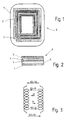
- Fig. 1 shows an embodiment of the invention
- Resonant circuit 6 in plan view. 2 is the in Fig. 1 shown resonant circuit 6 in cross section see.
- Deactivation of the resonant circuit 6 done by shorting between the two spiral Conductor tracks 2, 3, which are preferably made of aluminum are manufactured, through the dielectric layer 4 is produced.
- An applied alternating magnetic field, like it e.g. is emitted by the monitoring system AC voltages in the two spiral conductor tracks 2, 3 of the resonant circuit 6.
- the spiral Conductor tracks 2, 3 at least partially overlap and are in opposite directions wrapped.
- the exterior End of the lower coil 2 has a positive potential relative to inner end of the lower coil 2 when the inner end the upper coil 3 has a positive potential with respect to the has the outer end of the upper coil 3. So it stays to note that the points / areas in which the induced alternating voltages between the two coils 2, 3 are maximum, located in the end regions of the coils 2, 3.
- the upper coil 3 Since in the example shown in FIG. 1 the upper coil 3 has fewer turns than the lower coil 2, the highest voltages between the ends of the upper coil 3 and the positions directly below the lower coil 2 generated.
- Fig. 3 illustrates the voltage relationships in different areas of the two themselves at least partially overlapping coils 2, 3 of a resonant circuit 6, according to an advantageous development of the resonant circuit 6 according to the invention used can be.
- the dielectric layer 4 breaks open these local vulnerabilities together, although the potential for tension here is lower than at the ends of the top Coil 2 and lower coil 3. Since the voltage potential at the local vulnerabilities is less than at the ends of the Conductor tracks 2, 3 are those for generating the deactivation short circuit available electrical energy less than the electrical energy needed to generate one Deactivation short circuit at the ends of the upper coil 3 would be necessary.
- Fig. 5 shows a cross section through a dielectric Layer with manufacturing defects, here air bubbles 7 and Irregularities in the surface.
- the dielectric layer is to avoid manufacturing defects 4 trained according to a further training that they in essentially has a uniform thickness and large Part is free from local vulnerabilities 7.
- Such uniform dielectric layer 4 provides a Deactivation in the end areas of the spiral Conductor tracks 2, 3 safe, since here the induced voltage and Energy are maximum. A short circuit caused by a such deactivation arises, is very robust and little susceptible to inadvertent reactivation.
- the resonant circuit 6 consists of the dielectric layer 4 from at least two components 4a, 4b, an upper one Component 4a and a lower component 4b.
- the lower one Component 4b is stamped onto the lower coil 3 applied.
- the upper component 4a is on the upper coil 2 applied.
- the upper component has 4a a relatively low melting point, which allows her to serve as a hot melt adhesive and the two coils 2, 3 during the hot stamping of the upper coil 2 onto the lower one Glue coil 3.
- the upper component 4a of the dielectric Layer 4 melts during hot stamping of the top coil 2.
- the lower component 4b of the dielectric layer 4 has a higher melting point and does not melt during the Hot stamping on the top spool 2.
- the uniformity of the lower component 4b of the dielectric layer 4 which is not melts, improves the uniformity in the thickness of the dielectric layer 4 overall.
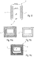
- Fig. 6 shows a cross section through a resonant circuit 6 with a dielectric layer 4 consisting of two Components 4a, 4b.
- the lower component 4b can either by coating the lower coil 3 or by Laminating the lower component 4b of the dielectric Layer 4 are produced on the coil 3.
- the coil material (A1) in the form of wide Roll material before, so that the uniformity of the surface the dielectric layer 4 can be maintained and other defects, for example, by Air pockets 7 are caused to be minimized.
- the resonant circuit 6 is local in the Area of the ends of the upper coil 2 or in the area of prepared area reinforced.
- the reinforced zone 10 is less prone to shear and glide or a Delaminate.
- everyone can Strain on the resonant circuit 6 by buckling or Bends are reduced because the two are spiral Conductor tracks 2, 3 only nearby, but not within the locally reinforced zone 10 shear, slide, kink or delaminate.
- Resonant circuit 6 are the areas around the ends one of the two conductor tracks 2, 3, here the upper one Conductor 2, reinforced by the fact that a local zone 10 with an additional pressure is applied, the metal, preferably aluminum, is shaped so that it is a non-plane Takes shape.
- the local pressurization causes better adhesion between the two conductor tracks 2, 3 and between the lower conductor track 3 and the dielectric layer 4. Is this pressure by means of a shaping tool 11 with a survey with a preset profile (stamp 12), the Traces 2,3 are shaped so that the resistance of the Resonant circuit 6 significantly against reactivation is improved.
- the tool 11 can also be flat be formed and have predetermined dimensions.
- Fig. 7 shows a plan view of an embodiment of a reinforced zone 10 at one end of the upper conductor track 2.
- Fig. 8a is a cross section and in Fig. 8b is a plan view a tool 11 shown for the manufacture of the reinforced zone 10 can be used.
- Training the weakened zone 13 can be done either by the Width of the conductor track 2, 3 is narrowed, as in FIG. 9 and Fig. 10, or by corresponding Treatment of the adhesive layer in this weakened zone 13, in such a way that the bond between the Conductor tracks 2, 3 is considerably weaker here.
- Another One way to get weakened zones 13 is to to perforate the conductor tracks 2, 3.
- FIG. 12 The equivalent circuit diagram of this arrangement is shown in FIG. 12 shown.
- the generated between the two coils 2, 3 Voltage difference is at the outer coil ends is much larger than anywhere else between the coils 2, 3.
- Figures 11c and 12 also show that the outer turn of the lower conductor track 3 from the upper To a large extent, conductor track 2 is not covered at all becomes.
- this overlap-free section 9 there is also no deactivation. If you follow them outer turn of the lower conductor track 3 from the end point back where there is a small overlap area with the upper trace 2 there, it is found that the next Point at which there is an overlap of the conductor tracks 2, 3 and thus there is a possibility of deactivation, one piece back on the outer turn of the lower conductor track 3 lies. This point has a much lower one Voltage potential between upper and lower conductor track 2, 3rd
- Another advantage is that due to the uneven distribution of the potential difference along the Conductor tracks 2, 3 for a deactivation short circuit available energy between the conductor tracks 2, 3 is higher must as with an even distribution of tension and Capacity. However, higher energy means one more reliable short circuit and thus also automatically less risk of unwanted reactivation.
Landscapes
- Physics & Mathematics (AREA)
- Engineering & Computer Science (AREA)
- Automation & Control Theory (AREA)
- Computer Security & Cryptography (AREA)
- Electromagnetism (AREA)
- General Physics & Mathematics (AREA)
- Burglar Alarm Systems (AREA)
- Coils Or Transformers For Communication (AREA)
- Emergency Protection Circuit Devices (AREA)
Claims (17)
- Elément de sécurité pour la protection électronique d'articles, se composant au moins d'une piste conductrice en spirale et d'un condensateur avec une couche diélectrique intercalée ou se composant de deux pistes conductrices en spirale qui sont disposées au moins partiellement en recouvrement des deux côtés d'une couche diélectrique,dont la couche diélectrique (4) comporte au moins une zone sélectionnée (8), dans laquelle un court-circuit est généré entre les plaques de condensateur opposées ou les pistes conductrices en spirale (2, 3), à raison d'un apport d'énergie suffisamment élevé par un champ magnétique alternatif,et dont la zone sélectionnée (8) est renforcée localement de manière à empêcher une destruction du court-circuit par sollicitation mécanique, et donc une réactivation de l'élément de sécurité (6).
- Elément de sécurité selon la revendication 1,
dont la couche diélectrique (4) présente essentiellement une épaisseur uniforme et n'a pas de défauts supplémentaires à la production. - Elément de sécurité selon la revendication 1 ou 2,
selon lequel, en cas de deux pistes conductrices en spirale (2, 3), tout au moins partiellement en recouvrement, celles-ci sont bobinées dans des directions opposées, la zone sélectionnée (8) se trouvant placée dans une zone aux extrémités externes des pistes conductrices (2, 3), étant donné que c'est là que se produit la tension d'induction la plus élevée. - Elément de sécurité selon la revendication 1,
dont la zone sélectionnée (8) se distingue par le fait que la couche diélectrique (4) est ici plus mince que dans les autres zones, ou qu'elle a un trou. - Elément de sécurité selon la revendication 1,
dont la zone sélectionnée (8) se distingue par le fait que la couche diélectrique (4) présente ici une autre propriété chimique ou physique que dans les autres zones. - Elément de sécurité selon la revendication 1 ou 2,
dont la couche diélectrique (4) se compose au moins de deux composants (4a, 4b). - Elément de sécurité selon la revendication 6,
dont l'un des composants (4a; 4b) de la couche diélectrique (4) présente un point de fusion supérieur à la température de production pour des éléments de sécurité (6). - Elément de sécurité selon la revendication 3,
dont les composants de la couche diélectrique (4) sont de nature à pouvoir être fabriqués soit par enduction soit par laminage. - Elément de sécurité selon la revendication 1, 3, 4 ou 5,
selon lequel le renforcement dans la zone renforcée (10) est obtenu par l'application d'une pression supplémentaire afin d'améliorer l'adhérence entre les plaques de condensateur ou entre les pistes conductrices au moins partiellement en recouvrement (2, 3). - Elément de sécurité selon la revendication 9,
dont la zone renforcée (10) est obtenue par moulage sous pression des plaques de condensateur ou des pistes conductrices au moins partiellement en recouvrement (2, 3) en forme tridimensionnelle. - Elément de sécurité selon la revendication 9 ou 10,
selon lequel l'adhérence améliorée et le moulage des plaques de condensateur ou des pistes conductrices (2, 3) sont obtenus en une seule opération. - Elément de sécurité selon la revendication 1, 3, 4 ou 5,
selon lequel des zones faiblement formées (13) sont prévues de deux côtés ou de l'autre côté de la zone sélectionnée (8). - Elément de sécurité selon la revendication 12,
dont les zones faiblement formées (13) sont formées par rétrécissement de la largeur de la piste conductrice (2; 3). - Elément de sécurité selon la revendication 12 ou 13,
dont la couche diélectrique (4) est dans les zones faiblement formées (13) moins fortement reliée avec les plaques de condensateur ou les pistes conductrices (2, 3) que dans les autres zones. - Elément de sécurité selon la revendication 12 ou 13,
dont les zones faiblement formées (13) se distinguent par le fait que les plaques de condensateur ou les pistes conductrices (2, 3) sont ici perforées. - Elément de sécurité selon la revendication 2,
dont les zones se recouvrant entre les deux pistes conductrices (2, 3) et donc la capacité entre les pistes conductrices (2, 3) se concentrent aux extrémités internes des pistes conductrices (2, 3). - Elément de sécurité selon la revendication 16,
dont les extrémités externes des deux pistes conductrices (2, 3) se recouvrent dans une petite zone, et une zone relativement longue, exempte de recouvrement (9), est adjacente aux extrémités externes des pistes conductrices (2, 3).
Applications Claiming Priority (5)
| Application Number | Priority Date | Filing Date | Title |
|---|---|---|---|
| DE19631775 | 1996-08-06 | ||
| DE19631775 | 1996-08-06 | ||
| DE19705723A DE19705723A1 (de) | 1996-08-06 | 1997-02-14 | Sicherungselement für die elektronische Artikelsicherung |
| DE19705723 | 1997-02-14 | ||
| PCT/EP1997/004116 WO1998006075A1 (fr) | 1996-08-06 | 1997-07-29 | Element antivol electronique |
Publications (2)
| Publication Number | Publication Date |
|---|---|
| EP0919050A1 EP0919050A1 (fr) | 1999-06-02 |
| EP0919050B1 true EP0919050B1 (fr) | 2000-03-22 |
Family
ID=26028183
Family Applications (1)
| Application Number | Title | Priority Date | Filing Date |
|---|---|---|---|
| EP97940042A Expired - Lifetime EP0919050B1 (fr) | 1996-08-06 | 1997-07-29 | Element antivol electronique |
Country Status (10)
| Country | Link |
|---|---|
| US (1) | US6262663B1 (fr) |
| EP (1) | EP0919050B1 (fr) |
| JP (1) | JP3634382B2 (fr) |
| AT (1) | ATE191095T1 (fr) |
| AU (1) | AU4203397A (fr) |
| CA (1) | CA2262573C (fr) |
| ES (1) | ES2147456T3 (fr) |
| NO (1) | NO313066B1 (fr) |
| PT (1) | PT919050E (fr) |
| WO (1) | WO1998006075A1 (fr) |
Cited By (1)
| Publication number | Priority date | Publication date | Assignee | Title |
|---|---|---|---|---|
| CN108806155A (zh) * | 2018-06-29 | 2018-11-13 | 仁怀市云侠网络科技有限公司 | 基于物联网的安防监控方法 |
Families Citing this family (8)
| Publication number | Priority date | Publication date | Assignee | Title |
|---|---|---|---|---|
| JP3390389B2 (ja) * | 1999-12-08 | 2003-03-24 | チェックポイント・マニュファクチュアリング・ジャパン株式会社 | 共振タグ |
| US6775839B1 (en) | 2002-03-15 | 2004-08-10 | O'brien Patrick J. | Optical storage device with print layer surface feature |
| JP2003317052A (ja) * | 2002-04-24 | 2003-11-07 | Smart Card:Kk | Icタグシステム |
| US7221275B2 (en) * | 2002-09-03 | 2007-05-22 | Massachusetts Institute Of Technology | Tuneable wireless tags using spatially inhomogeneous structures |
| US7355516B2 (en) * | 2004-12-23 | 2008-04-08 | Checkpoint Systems, Inc. | Method and apparatus for protecting culinary products |
| WO2007130147A2 (fr) * | 2005-11-04 | 2007-11-15 | Gerald Giasson | Système de capteur de sécurité |
| US8125341B2 (en) * | 2007-12-10 | 2012-02-28 | Checkpoint Systems, Inc. | Resonant tag with reinforced deactivation dimple |
| WO2010066955A1 (fr) | 2008-12-11 | 2010-06-17 | Yves Eray | Circuit d'antenne rfid |
Family Cites Families (8)
| Publication number | Priority date | Publication date | Assignee | Title |
|---|---|---|---|---|
| US3967161A (en) | 1972-06-14 | 1976-06-29 | Lichtblau G J | A multi-frequency resonant tag circuit for use with an electronic security system having improved noise discrimination |
| US4498076A (en) | 1982-05-10 | 1985-02-05 | Lichtblau G J | Resonant tag and deactivator for use in an electronic security system |
| US4876555B1 (en) * | 1987-03-17 | 1995-07-25 | Actron Entwicklungs Ag | Resonance label and method for its fabrication |
| DK0458923T3 (da) | 1989-12-20 | 1995-05-08 | Actron Entwicklungs Ag | Deaktiverbar resonansetikette |
| CH682957A5 (de) | 1991-04-16 | 1993-12-15 | Kobe Properties Ltd | Verfahren zur Deaktivierung einer Resonanz-Etikette. |
| NL9202067A (nl) | 1992-11-27 | 1994-06-16 | Dutch A & A Trading Bv | Detectielabel. |
| US5510770A (en) | 1994-03-30 | 1996-04-23 | Checkpoint Systems, Inc. | Surface deactivateable tag |
| EP0755036A1 (fr) | 1995-07-20 | 1997-01-22 | Esselte Meto International GmbH | Etiquette à résonance déactivable et procédé de sa fabrication |
-
1997
- 1997-07-29 JP JP50756898A patent/JP3634382B2/ja not_active Expired - Fee Related
- 1997-07-29 WO PCT/EP1997/004116 patent/WO1998006075A1/fr not_active Ceased
- 1997-07-29 PT PT97940042T patent/PT919050E/pt unknown
- 1997-07-29 AU AU42033/97A patent/AU4203397A/en not_active Abandoned
- 1997-07-29 ES ES97940042T patent/ES2147456T3/es not_active Expired - Lifetime
- 1997-07-29 CA CA002262573A patent/CA2262573C/fr not_active Expired - Fee Related
- 1997-07-29 EP EP97940042A patent/EP0919050B1/fr not_active Expired - Lifetime
- 1997-07-29 AT AT97940042T patent/ATE191095T1/de not_active IP Right Cessation
- 1997-07-29 US US09/147,646 patent/US6262663B1/en not_active Expired - Lifetime
-
1999
- 1999-02-04 NO NO19990517A patent/NO313066B1/no not_active IP Right Cessation
Cited By (2)
| Publication number | Priority date | Publication date | Assignee | Title |
|---|---|---|---|---|
| CN108806155A (zh) * | 2018-06-29 | 2018-11-13 | 仁怀市云侠网络科技有限公司 | 基于物联网的安防监控方法 |
| CN108806155B (zh) * | 2018-06-29 | 2020-02-11 | 仁怀市云侠网络科技有限公司 | 基于物联网的安防监控方法 |
Also Published As
| Publication number | Publication date |
|---|---|
| ATE191095T1 (de) | 2000-04-15 |
| NO990517D0 (no) | 1999-02-04 |
| CA2262573A1 (fr) | 1998-02-12 |
| EP0919050A1 (fr) | 1999-06-02 |
| WO1998006075A1 (fr) | 1998-02-12 |
| PT919050E (pt) | 2000-08-31 |
| AU4203397A (en) | 1998-02-25 |
| US6262663B1 (en) | 2001-07-17 |
| CA2262573C (fr) | 2002-04-16 |
| JP3634382B2 (ja) | 2005-03-30 |
| JP2001504604A (ja) | 2001-04-03 |
| NO313066B1 (no) | 2002-08-05 |
| NO990517L (no) | 1999-02-04 |
| ES2147456T3 (es) | 2000-09-01 |
Similar Documents
| Publication | Publication Date | Title |
|---|---|---|
| DE60124900T2 (de) | Aktivierbares/deaktivierbares sicherheitsetikett mit einem verbesserten elektrostatischen schutz zur verwendung mit einem elektronischen sicherheitssystem | |
| DE69616709T2 (de) | Deaktivierbares Sicherheitsetikett | |
| DE69427641T2 (de) | Mehrfrequenz-etikett | |
| DE19733849C2 (de) | Diebstahlsicherungsschild | |
| DE69518261T2 (de) | Resonanzetiketten und Herstellungsverfahren | |
| EP0092555B1 (fr) | Dispositif d'identification en forme d une etiquette pour l attacher a un objet | |
| DE69836650T2 (de) | Fuseanordnung | |
| DE69021743T2 (de) | Resonanzaufkleber sowie Verfahren zur Herstellung. | |
| DE69228483T2 (de) | Sicherheitsetikett mit elektrostatischem schutz | |
| DE69223321T2 (de) | Etikette gegen diebstahl | |
| DE4129446C2 (de) | Desaktivierbare elektronische Artikelüberwachungsetiketten, Etikettenbänder und Verfahren zum Herstellen von Etikettenbändern | |
| EP0919050B1 (fr) | Element antivol electronique | |
| CH680823A5 (fr) | ||
| EP0919049B1 (fr) | Circuit a resonance pour element antivol electronique | |
| EP0260330A1 (fr) | Protection antivol pour objets | |
| DE19705723A1 (de) | Sicherungselement für die elektronische Artikelsicherung | |
| EP1224640B1 (fr) | Element de securite antivol pour la securite antivol electronique d'articles | |
| EP0810567B1 (fr) | Dispositif et procédé pour protéger un article contre le vol | |
| EP1017033B1 (fr) | Elément pour la protection électronique d'articles et procédé de fabrication | |
| EP0252071A1 (fr) | Dispositif analogue a une etiquette et son procede de fabrication | |
| EP0935767B1 (fr) | Elements de securite pour la surveillance electronique d'articles | |
| DE19708180A1 (de) | Sicherungselement für die elektronische Artikelüberwachung | |
| EP0941531B1 (fr) | Systeme antivol, notamment pour textiles, cuirs, ou similaire | |
| DE29814277U1 (de) | Sicherungselement für die elektronische Artikelsicherung | |
| DE19908877A1 (de) | Warensicherungsetikett und Verfahren zu seiner Herstellung |
Legal Events
| Date | Code | Title | Description |
|---|---|---|---|
| PUAI | Public reference made under article 153(3) epc to a published international application that has entered the european phase |
Free format text: ORIGINAL CODE: 0009012 |
|
| 17P | Request for examination filed |
Effective date: 19981127 |
|
| AK | Designated contracting states |
Kind code of ref document: A1 Designated state(s): AT BE CH DE DK ES FI FR GB IT LI NL PT SE |
|
| GRAG | Despatch of communication of intention to grant |
Free format text: ORIGINAL CODE: EPIDOS AGRA |
|
| GRAG | Despatch of communication of intention to grant |
Free format text: ORIGINAL CODE: EPIDOS AGRA |
|
| GRAH | Despatch of communication of intention to grant a patent |
Free format text: ORIGINAL CODE: EPIDOS IGRA |
|
| 17Q | First examination report despatched |
Effective date: 19990812 |
|
| GRAH | Despatch of communication of intention to grant a patent |
Free format text: ORIGINAL CODE: EPIDOS IGRA |
|
| GRAA | (expected) grant |
Free format text: ORIGINAL CODE: 0009210 |
|
| AK | Designated contracting states |
Kind code of ref document: B1 Designated state(s): AT BE CH DE DK ES FI FR GB IT LI NL PT SE |
|
| REF | Corresponds to: |
Ref document number: 191095 Country of ref document: AT Date of ref document: 20000415 Kind code of ref document: T |
|
| REG | Reference to a national code |
Ref country code: CH Ref legal event code: EP |
|
| REF | Corresponds to: |
Ref document number: 59701333 Country of ref document: DE Date of ref document: 20000427 |
|
| ITF | It: translation for a ep patent filed | ||
| GBT | Gb: translation of ep patent filed (gb section 77(6)(a)/1977) |
Effective date: 20000517 |
|
| ET | Fr: translation filed | ||
| REG | Reference to a national code |
Ref country code: CH Ref legal event code: NV Representative=s name: OK PAT AG |
|
| REG | Reference to a national code |
Ref country code: DK Ref legal event code: T3 |
|
| REG | Reference to a national code |
Ref country code: PT Ref legal event code: SC4A Free format text: AVAILABILITY OF NATIONAL TRANSLATION Effective date: 20000530 |
|
| REG | Reference to a national code |
Ref country code: ES Ref legal event code: FG2A Ref document number: 2147456 Country of ref document: ES Kind code of ref document: T3 |
|
| NLR4 | Nl: receipt of corrected translation in the netherlands language at the initiative of the proprietor of the patent | ||
| PLBE | No opposition filed within time limit |
Free format text: ORIGINAL CODE: 0009261 |
|
| STAA | Information on the status of an ep patent application or granted ep patent |
Free format text: STATUS: NO OPPOSITION FILED WITHIN TIME LIMIT |
|
| 26N | No opposition filed | ||
| REG | Reference to a national code |
Ref country code: GB Ref legal event code: IF02 |
|
| PGFP | Annual fee paid to national office [announced via postgrant information from national office to epo] |
Ref country code: AT Payment date: 20040702 Year of fee payment: 8 |
|
| PGFP | Annual fee paid to national office [announced via postgrant information from national office to epo] |
Ref country code: PT Payment date: 20040705 Year of fee payment: 8 |
|
| PGFP | Annual fee paid to national office [announced via postgrant information from national office to epo] |
Ref country code: FI Payment date: 20040722 Year of fee payment: 8 Ref country code: DK Payment date: 20040722 Year of fee payment: 8 |
|
| PG25 | Lapsed in a contracting state [announced via postgrant information from national office to epo] |
Ref country code: FI Free format text: LAPSE BECAUSE OF NON-PAYMENT OF DUE FEES Effective date: 20050710 |
|
| PG25 | Lapsed in a contracting state [announced via postgrant information from national office to epo] |
Ref country code: AT Free format text: LAPSE BECAUSE OF NON-PAYMENT OF DUE FEES Effective date: 20050729 |
|
| PG25 | Lapsed in a contracting state [announced via postgrant information from national office to epo] |
Ref country code: DK Free format text: LAPSE BECAUSE OF NON-PAYMENT OF DUE FEES Effective date: 20050801 |
|
| PG25 | Lapsed in a contracting state [announced via postgrant information from national office to epo] |
Ref country code: PT Free format text: LAPSE BECAUSE OF NON-PAYMENT OF DUE FEES Effective date: 20060130 |
|
| REG | Reference to a national code |
Ref country code: DK Ref legal event code: EBP |
|
| PGFP | Annual fee paid to national office [announced via postgrant information from national office to epo] |
Ref country code: CH Payment date: 20070730 Year of fee payment: 11 |
|
| PGFP | Annual fee paid to national office [announced via postgrant information from national office to epo] |
Ref country code: SE Payment date: 20070727 Year of fee payment: 11 |
|
| REG | Reference to a national code |
Ref country code: CH Ref legal event code: PL |
|
| EUG | Se: european patent has lapsed | ||
| PG25 | Lapsed in a contracting state [announced via postgrant information from national office to epo] |
Ref country code: LI Free format text: LAPSE BECAUSE OF NON-PAYMENT OF DUE FEES Effective date: 20080731 Ref country code: CH Free format text: LAPSE BECAUSE OF NON-PAYMENT OF DUE FEES Effective date: 20080731 |
|
| PG25 | Lapsed in a contracting state [announced via postgrant information from national office to epo] |
Ref country code: SE Free format text: LAPSE BECAUSE OF NON-PAYMENT OF DUE FEES Effective date: 20080730 |
|
| REG | Reference to a national code |
Ref country code: DE Ref legal event code: R082 Ref document number: 59701333 Country of ref document: DE |
|
| PGFP | Annual fee paid to national office [announced via postgrant information from national office to epo] |
Ref country code: BE Payment date: 20130712 Year of fee payment: 17 |
|
| PGFP | Annual fee paid to national office [announced via postgrant information from national office to epo] |
Ref country code: IT Payment date: 20130717 Year of fee payment: 17 |
|
| PG25 | Lapsed in a contracting state [announced via postgrant information from national office to epo] |
Ref country code: IT Free format text: LAPSE BECAUSE OF NON-PAYMENT OF DUE FEES Effective date: 20140729 |
|
| REG | Reference to a national code |
Ref country code: FR Ref legal event code: PLFP Year of fee payment: 20 |
|
| PGFP | Annual fee paid to national office [announced via postgrant information from national office to epo] |
Ref country code: ES Payment date: 20160613 Year of fee payment: 20 |
|
| PGFP | Annual fee paid to national office [announced via postgrant information from national office to epo] |
Ref country code: FR Payment date: 20160613 Year of fee payment: 20 |
|
| PGFP | Annual fee paid to national office [announced via postgrant information from national office to epo] |
Ref country code: NL Payment date: 20160711 Year of fee payment: 20 |
|
| PGFP | Annual fee paid to national office [announced via postgrant information from national office to epo] |
Ref country code: DE Payment date: 20160726 Year of fee payment: 20 Ref country code: GB Payment date: 20160727 Year of fee payment: 20 |
|
| REG | Reference to a national code |
Ref country code: DE Ref legal event code: R071 Ref document number: 59701333 Country of ref document: DE |
|
| PG25 | Lapsed in a contracting state [announced via postgrant information from national office to epo] |
Ref country code: BE Free format text: LAPSE BECAUSE OF NON-PAYMENT OF DUE FEES Effective date: 20140731 |
|
| REG | Reference to a national code |
Ref country code: NL Ref legal event code: MK Effective date: 20170728 |
|
| REG | Reference to a national code |
Ref country code: GB Ref legal event code: PE20 Expiry date: 20170728 |
|
| PG25 | Lapsed in a contracting state [announced via postgrant information from national office to epo] |
Ref country code: GB Free format text: LAPSE BECAUSE OF EXPIRATION OF PROTECTION Effective date: 20170728 |
|
| REG | Reference to a national code |
Ref country code: ES Ref legal event code: FD2A Effective date: 20180508 |
|
| PG25 | Lapsed in a contracting state [announced via postgrant information from national office to epo] |
Ref country code: ES Free format text: LAPSE BECAUSE OF EXPIRATION OF PROTECTION Effective date: 20170730 |