EP0919917A2 - Verfahren zum Testen des Pufferspeichers eines Mikroprozessorsystems - Google Patents
Verfahren zum Testen des Pufferspeichers eines Mikroprozessorsystems Download PDFInfo
- Publication number
- EP0919917A2 EP0919917A2 EP98440220A EP98440220A EP0919917A2 EP 0919917 A2 EP0919917 A2 EP 0919917A2 EP 98440220 A EP98440220 A EP 98440220A EP 98440220 A EP98440220 A EP 98440220A EP 0919917 A2 EP0919917 A2 EP 0919917A2
- Authority
- EP
- European Patent Office
- Prior art keywords
- memory
- microprocessor
- buffer
- buffer memory
- test
- Prior art date
- Legal status (The legal status is an assumption and is not a legal conclusion. Google has not performed a legal analysis and makes no representation as to the accuracy of the status listed.)
- Granted
Links
Images

Classifications
-
- G—PHYSICS
- G06—COMPUTING OR CALCULATING; COUNTING
- G06F—ELECTRIC DIGITAL DATA PROCESSING
- G06F11/00—Error detection; Error correction; Monitoring
- G06F11/22—Detection or location of defective computer hardware by testing during standby operation or during idle time, e.g. start-up testing
- G06F11/2205—Detection or location of defective computer hardware by testing during standby operation or during idle time, e.g. start-up testing using arrangements specific to the hardware being tested
- G06F11/2236—Detection or location of defective computer hardware by testing during standby operation or during idle time, e.g. start-up testing using arrangements specific to the hardware being tested to test CPU or processors
-
- G—PHYSICS
- G06—COMPUTING OR CALCULATING; COUNTING
- G06F—ELECTRIC DIGITAL DATA PROCESSING
- G06F11/00—Error detection; Error correction; Monitoring
- G06F11/07—Responding to the occurrence of a fault, e.g. fault tolerance
- G06F11/16—Error detection or correction of the data by redundancy in hardware
- G06F11/1666—Error detection or correction of the data by redundancy in hardware where the redundant component is memory or memory area
- G06F11/167—Error detection by comparing the memory output
-
- G—PHYSICS
- G11—INFORMATION STORAGE
- G11C—STATIC STORES
- G11C29/00—Checking stores for correct operation ; Subsequent repair; Testing stores during standby or offline operation
- G11C29/04—Detection or location of defective memory elements, e.g. cell constructio details, timing of test signals
- G11C29/08—Functional testing, e.g. testing during refresh, power-on self testing [POST] or distributed testing
Definitions
- the invention relates to a method for testing the buffer memory of a microprocessor system.
- Buffer memories which are often also referred to as caches, are located in this Hierarchy between main memories and register memories. You have the Task, the current main memory contents during a program execution available to the microprocessor as quickly as possible as “copies" to deliver.
- the buffer memories are either located directly on the microprocessor chip (so-called “first-level” or “on-chip cache”) or are independent Blocks ("second level cache”).
- a memory cell permanently assume a fixed value (zero or one) without this can be changed again by overwriting.
- One such, also called a "stuck-at" error designated error behavior can be caused, for example, by a short circuit within of the memory cell.
- a microprocessor that performs read operations executes on such a faulty buffer memory incorrect data and usually determines incorrect results from it.
- the invention solves this problem with the help of that specified in claim 1 Characteristics.
- the content of the buffer memory with the content a reference memory compared.
- the comparison can be made without data or commands from the program running in the foreground modified or even overwritten. So that's the procedure suitable while the microprocessor system is running in the background to expire. Because especially microprocessor systems in safety-critical Applications are often in operation for a very long time without interruption, errors that occur during operation can be detected very reliably and initiate suitable measures (warnings etc.). this leads to a significant increase in security.
- the reference memory a register memory. Additional memory modules for the reference memory are not required in this embodiment.
- the test is based on a test bit pattern specially selected for test purposes.
- the Using special test bit patterns has an advantageous effect on reliability of the test.
- the microprocessor system MPS comprises a microprocessor CPU, one Buffer memory CM, a main memory MM and an input / output unit 1 / O.
- the addressing between the microprocessor, the main memory and the input / output unit is via an ABUS address bus.
- the buffer memory is mostly CM with its own address and data bus ABUSC or DBUSC with the microprocessor connected.
- the buffer memory CM can be one in common with the microprocessor "first-level" arranged on a chip Buffer memory or a "second-level" built up independently of it Act buffer storage.
- microprocessor systems that both have a "first-level” as well as a “second-level” buffer memory. On such microprocessor systems are briefly discussed below.
- memory management unit memory management unit
- CM and a reference memory the z. B. a register memory belonging to the microprocessor can be the same data is written. Subsequently the data from the two memories are read out again and by the microprocessor The CPU then checks whether they match. If the microprocessor If no match is found, there is an error in the Buffer memory before, provided that the reference memory is functioning properly can run out (e.g. due to additional tests for the Reference memory). From the exemplary embodiments described below it becomes clear what options are available when carrying out the test consist.
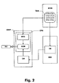
- Fig. 2 shows a main memory MM and a chip CHIP, on which a "first level" Buffer memory CM and a microprocessor CPU are arranged.
- the microprocessor includes a register memory REG and the actual ones Processing units.
- the exchange of addresses and data between the individual Components are carried out via an address bus or a, as explained above Data bus, but for the sake of clarity just like the processing units are not shown.
- the arrows in Fig. 2 only indicate the flow of information between the components.
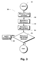
- Fig. 3 shows a flow diagram in which the most important steps in the implementation of buffer test 30 are shown.
- the bufferable buffer IM can be a memory module intended specifically for test purposes.
- an area of the Main memory MM defined as a buffer IM.
- the storage capacity of the buffer IM corresponds exactly to the size of the buffer memory to be tested CM.
- test bit pattern TBM is then removed from the buffer in a step 33 IM copied into the buffer memory CM. This is preferably done that the microprocessor CPU has a read access to the test bit pattern TBM performs what this from the buffer IM in the buffer memory CM is copied.
- the details of this copy process depend on type of microprocessor used. In an exemplary embodiment explained below, which relates to a specific microprocessor discussed this point again.
- the test bit pattern TBM becomes non-rewritable Memory ROM written out in the reference memory REG.
- the reference memory REG is preferably one for Microprocessor CPU-owned register memory. However, it is also possible For this purpose, a specially designed memory module use.
- the microprocessor CPU then compares in one step 35 the test bit pattern from the buffer memory CM with that in the reference memory REG stored test bit pattern TBM. This comparison is shown in FIG the reference symbol XOR. If the buffer memory is working properly CM must match the two test bit patterns. voices If the two test bit patterns do not match, the microprocessor causes the CPU in a step 36 the execution of an error action FH. What a mistake to be carried out in detail depends on the purpose of the microprocessor system. With redundant microprocessor systems, such as those used in aircraft or signal boxes, the error action could be one identified as incorrect Microprocessor system from the other faultless microprocessor systems isolate.
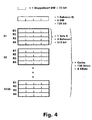
- This buffer memory is a so-called “four-way set associative cache” designed.
- 4 is the buffer memory architecture of this microprocessor outlined.
- the program module which controls the execution of the test method according to the invention is loaded into a memory area declared as non-bufferable. This ensures that program instructions are not buffered during the execution of the test and therefore cannot interfere with the test.
- This memory area not declared as bufferable can be, for example, an area of a non-rewritable memory ROM (see FIG. 2).
- Each memory cell of this buffer IM is filled with a 32-bit test bit pattern, which is preferably also stored in the non-rewritable memory ROM.
- Suitable test bit patterns are e.g. B. CENELEC standard "Railway Applications: Safety-Related Electronic Railway Control and Protection Systems," CENELEC pr EN 50129 Draft 7 (1993), can be removed. To avoid an interruption during the execution of the test, all interrupts are overridden; Furthermore, the contents of the buffer memory are now considered to be "flushed”.
- the memory management is designed so that at Read accesses of the microprocessor is first checked to see if one is specified Main memory address belonging entry in the buffer memory. If if this is the case, the microprocessor reads the entry from the buffer memory. If, on the other hand, there is no corresponding entry in the buffer memory, it will Date copied from the main memory into the buffer memory and also the Microprocessor supplied. The microprocessor only reads after a second read access the date directly from the buffer memory, unless the date has already been overwritten.
- the TBM test bit pattern cannot be read by a single read be copied into the buffer memory CM. Rather, the buffer memory CM frame by frame with the test bit pattern from the IM area Main memory MM filled up. This is because addressing of the buffer memory on the INTEL® i486 as on most others Microprocessors is frame-oriented. The frame orientation has Consequence that not only a requested double word, but an entire frame of four double words is loaded in advance ("data prefetch"). Since the Buffer memory of the INTEL® i486 as shown in Fig. 4 a total of 128 frames 128 reads are therefore required to access the buffer memory completely fill with the test bit pattern.
- the test bit pattern TBM After filling the buffer memory CM with the test bit pattern TBM the test bit pattern TBM stored in the non-rewritable memory ROM a register memory REG of the microprocessor which serves as a reference memory CPU copied. Basically, it is also possible to copy this process also before filling the buffer tank.
- the buffer memory CM is completely filled and then frame by frame with the contents of the reference memory compared. It is of course also possible to start with just one frame to fill the buffer memory CM with the test bit pattern TBM, this with the Compare the contents of the reference memory REG, then the next one Fill the frame of the buffer memory and with the content of the reference memory to compare, etc. With this alternative approach, the buffer memory So do not fully fill up first before comparing comes with the content of the reference memory. Rather, the replenishment and the comparison carried out in constant change.
- microprocessor system instead of a "first level” a “second level” Buffer memory, it can be tested in the same way as above described.
- first level a "second level” Buffer memory
- second-level buffer memory is only for that Make sure that each of the two buffer memories is tested individually. Preferably this is achieved in that before testing the one buffer memory the other is deactivated.
Landscapes
- Engineering & Computer Science (AREA)
- General Engineering & Computer Science (AREA)
- Theoretical Computer Science (AREA)
- Computer Hardware Design (AREA)
- Quality & Reliability (AREA)
- Physics & Mathematics (AREA)
- General Physics & Mathematics (AREA)
- Techniques For Improving Reliability Of Storages (AREA)
- Memory System Of A Hierarchy Structure (AREA)
Abstract
Description
Claims (9)
- Verfahren zum Testen des Pufferspeichers (CM in Fig. 2) eines Mikroprozessorsystems,
dadurch gekennzeichnet,
daß der Inhalt des Pufferspeichers (CM) mit dem Inhalt eines Referenzspeichers (REG) verglichen wird. - Verfahren nach Anspruch 1, bei dem der Referenzspeicher (REG) ein Registerspeicher ist.
- Verfahren nach einem der vorhergehenden Ansprüche mit folgenden Schritten:a) ein Test-Bitmuster (TBM) wird in einen Zwischenspeicher (IM) geschrieben (32),b) das Test-Bitmuster (TBM) wird vom Zwischenspeicher (IM) in den zu testenden Pufferspeicher (CM) kopiert (33),c) das Test-Bitmuster (TBM) wird in den Referenzspeicher (REG) kopiert (34),d) der Mikroprozessor (CPU) prüft, ob das in den Pufferspeicher (CM) kopierte Test-Bitmuster mit dem in den Referenzpeicher (REG) kopierten Test-Bitmuster übereinstimmt (35),e) der Mikroprozessor (CPU) veranlaßt die Durchführung einer Fehlerhandlung (36), sofern bei der Prüfung nach d) keine Übereinstimmung festgestellt wird.
- Verfahren nach Anspruch 3, bei dem der Zwischenspeicher (IM) ein pufferbarer Bereich eines Hauptspeichers (MM) des Mikroprozessorsystems ist.
- Verfahren nach Anspruch 3, bei dem die Überprüfung nach Schritt d) mit Hilfe einer Bool'schen XOR-Operation durchgeführt wird.
- Verfahren nach einem der vorhergehenden Ansprüche, bei dem der zu testende Pufferspeicher (CM) sich auf demselben Chip (CHIP) wie der Mikroprozessor (CPU) befindet.
- Verfahren nach einem der vorhergehenden Ansprüche, bei dem das Programmodul zur Steuerung des Tests in einem nicht überschreibbaren und nicht pufferbaren Speicher (ROM) gespeichert ist.
- Programmodul mit einer Anzahl von Steuerbefehlen,
dadurch gekennzeichnet,
daß die Steuerbefehle so angeordnet sind, daß sie ein Verfahren nach einem der vorhergehenden Ansprüche steuern. - Datenträger, auf dem ein Programmodul nach Anspruch 8 gespeichert ist.
Applications Claiming Priority (2)
| Application Number | Priority Date | Filing Date | Title |
|---|---|---|---|
| DE19749240A DE19749240A1 (de) | 1997-11-07 | 1997-11-07 | Verfahren zum Testen des Pufferspeichers eines Mikroprozessorsystems |
| DE19749240 | 1997-11-07 |
Publications (3)
| Publication Number | Publication Date |
|---|---|
| EP0919917A2 true EP0919917A2 (de) | 1999-06-02 |
| EP0919917A3 EP0919917A3 (de) | 1999-12-22 |
| EP0919917B1 EP0919917B1 (de) | 2003-01-22 |
Family
ID=7847931
Family Applications (1)
| Application Number | Title | Priority Date | Filing Date |
|---|---|---|---|
| EP98440220A Expired - Lifetime EP0919917B1 (de) | 1997-11-07 | 1998-10-09 | Verfahren zum Testen des Pufferspeichers eines Mikroprozessorsystems |
Country Status (3)
| Country | Link |
|---|---|
| EP (1) | EP0919917B1 (de) |
| AT (1) | ATE231631T1 (de) |
| DE (2) | DE19749240A1 (de) |
Cited By (1)
| Publication number | Priority date | Publication date | Assignee | Title |
|---|---|---|---|---|
| FR2919401A1 (fr) * | 2007-07-24 | 2009-01-30 | Thales Sa | Procede de test des chemins de donnees dans un circuit electronique |
Families Citing this family (1)
| Publication number | Priority date | Publication date | Assignee | Title |
|---|---|---|---|---|
| DE10120668A1 (de) | 2001-04-27 | 2002-11-07 | Infineon Technologies Ag | Verfahren zum Testen der Datenaustausch-Funktionsfähigkeit eines Speichers |
Family Cites Families (2)
| Publication number | Priority date | Publication date | Assignee | Title |
|---|---|---|---|---|
| US5680544A (en) * | 1995-09-05 | 1997-10-21 | Digital Equipment Corporation | Method for testing an on-chip cache for repair |
| DE19639613A1 (de) * | 1996-09-26 | 1997-08-14 | Siemens Ag | Integrierter Speicher und Paralleltest-Schaltungsanordnung |
-
1997
- 1997-11-07 DE DE19749240A patent/DE19749240A1/de not_active Withdrawn
-
1998
- 1998-10-09 DE DE59806993T patent/DE59806993D1/de not_active Expired - Lifetime
- 1998-10-09 AT AT98440220T patent/ATE231631T1/de not_active IP Right Cessation
- 1998-10-09 EP EP98440220A patent/EP0919917B1/de not_active Expired - Lifetime
Cited By (2)
| Publication number | Priority date | Publication date | Assignee | Title |
|---|---|---|---|---|
| FR2919401A1 (fr) * | 2007-07-24 | 2009-01-30 | Thales Sa | Procede de test des chemins de donnees dans un circuit electronique |
| US7913129B2 (en) | 2007-07-24 | 2011-03-22 | Thales | Method of testing data paths in an electronic circuit |
Also Published As
| Publication number | Publication date |
|---|---|
| ATE231631T1 (de) | 2003-02-15 |
| EP0919917A3 (de) | 1999-12-22 |
| DE59806993D1 (de) | 2003-02-27 |
| EP0919917B1 (de) | 2003-01-22 |
| DE19749240A1 (de) | 1999-05-12 |
Similar Documents
| Publication | Publication Date | Title |
|---|---|---|
| DE3876459T2 (de) | Speicher und deren pruefung. | |
| DE2225841C3 (de) | Verfahren und Anordnung zur systematischen Fehlerprüfung eines monolithischen Halbleiterspeichers | |
| DE19800311A1 (de) | Elektronische, digitale Einrichtung | |
| EP0046976A2 (de) | Halbleiterspeicher aus Speicherbausteinen mit redundanten Speicherbereichen | |
| DE112007003015T5 (de) | Verfahren und Vorrichtung zur Cache-gestützten Fehlerdetektion und -korrektur in einem Speicher | |
| DE68922440T2 (de) | Gerät und Verfahren zur gleichzeitigen Einreichung von Fehlerunterbrechung und Fehlerdaten zu einem Unterstützungsprozessor. | |
| EP1113362B1 (de) | Integrierter Halbleiterspeicher mit einer Speichereinheit zum Speichern von Adressen fehlerhafter Speicherzellen | |
| DE19835610A1 (de) | Programmgesteuerte Einheit und Verfahren zum Debuggen derselben | |
| DE69715993T2 (de) | Cache-Speicher mit Verwendung fehlerhaften Ettikettenspeichers | |
| DE3814875C2 (de) | ||
| EP1055238B1 (de) | Testschaltung und verfahren zum prüfen einer digitalen halbleiter-schaltungsanordnung | |
| DE10256487B4 (de) | Integrierter Speicher und Verfahren zum Testen eines integrierten Speichers | |
| EP0990236B1 (de) | Anordnung mit speicherzellen und verfahren zur funktionsüberprüfung von speicherzellen | |
| WO2005078586A2 (de) | Einrichtung und verfahren zur analyse von eingebetteten systemen für sicherheitskritische rechnersysteme in kraftfahrzeugen | |
| EP0919917B1 (de) | Verfahren zum Testen des Pufferspeichers eines Mikroprozessorsystems | |
| DE4227784A1 (de) | Rechnersystem und verfahren zum beheben eines seitenfehlers | |
| DE2823457C2 (de) | Schaltungsanordnung zur Fehlerüberwachung eines Speichers einer digitalen Rechenanlage | |
| DE102004043063A1 (de) | Halbleiter-Bauelement mit Test-Schnittstellen-Einrichtung | |
| WO1988009554A1 (fr) | Procede et agencement de controle automatique de memoires vives organisees par mots | |
| DE102005018790A1 (de) | Integrierter Schaltkreis und Verfahren zum Betreiben und parallelen Testen von integrierten Schaltkreisen | |
| DE102005060901A1 (de) | Verfahren zur Erkennung einer Versorgungsunterbrechung in einem Datenspeicher und zur Wiederherstellung des Datenspeichers | |
| DE102005037226A1 (de) | Verfahren und Vorrichtung zur Festlegung eines Startzustandes bei einem Rechnersystem mit wenigstens zwei Ausführungseinheiten durch markieren von Registern | |
| DE102006036384A1 (de) | Mikroprozessorsystem zur Steuerung bzw. Regelung von zumindest zum Teil sicherheitskritischen Prozessen | |
| DE10334520B4 (de) | Verfahren und Vorrichtung zur Fehlerkorrektur bei einem digitalen Speicher | |
| DE3817857C2 (de) |
Legal Events
| Date | Code | Title | Description |
|---|---|---|---|
| PUAI | Public reference made under article 153(3) epc to a published international application that has entered the european phase |
Free format text: ORIGINAL CODE: 0009012 |
|
| AK | Designated contracting states |
Kind code of ref document: A2 Designated state(s): AT BE CH DE DK ES FI FR GB IT LI NL PT SE |
|
| AX | Request for extension of the european patent |
Free format text: AL;LT;LV;MK;RO;SI |
|
| PUAL | Search report despatched |
Free format text: ORIGINAL CODE: 0009013 |
|
| AK | Designated contracting states |
Kind code of ref document: A3 Designated state(s): AT BE CH CY DE DK ES FI FR GB GR IE IT LI LU MC NL PT SE |
|
| AX | Request for extension of the european patent |
Free format text: AL;LT;LV;MK;RO;SI |
|
| 17P | Request for examination filed |
Effective date: 20000212 |
|
| AKX | Designation fees paid |
Free format text: AT BE CH DE DK ES FI FR GB IT LI NL PT SE |
|
| 17Q | First examination report despatched |
Effective date: 20020117 |
|
| GRAH | Despatch of communication of intention to grant a patent |
Free format text: ORIGINAL CODE: EPIDOS IGRA |
|
| GRAH | Despatch of communication of intention to grant a patent |
Free format text: ORIGINAL CODE: EPIDOS IGRA |
|
| GRAA | (expected) grant |
Free format text: ORIGINAL CODE: 0009210 |
|
| AK | Designated contracting states |
Kind code of ref document: B1 Designated state(s): AT BE CH DE DK ES FI FR GB IT LI NL PT SE |
|
| PG25 | Lapsed in a contracting state [announced via postgrant information from national office to epo] |
Ref country code: NL Free format text: LAPSE BECAUSE OF FAILURE TO SUBMIT A TRANSLATION OF THE DESCRIPTION OR TO PAY THE FEE WITHIN THE PRESCRIBED TIME-LIMIT Effective date: 20030122 Ref country code: FI Free format text: LAPSE BECAUSE OF FAILURE TO SUBMIT A TRANSLATION OF THE DESCRIPTION OR TO PAY THE FEE WITHIN THE PRESCRIBED TIME-LIMIT Effective date: 20030122 |
|
| REG | Reference to a national code |
Ref country code: GB Ref legal event code: FG4D Free format text: NOT ENGLISH |
|
| REG | Reference to a national code |
Ref country code: CH Ref legal event code: EP |
|
| REF | Corresponds to: |
Ref document number: 59806993 Country of ref document: DE Date of ref document: 20030227 Kind code of ref document: P |
|
| GBT | Gb: translation of ep patent filed (gb section 77(6)(a)/1977) |
Effective date: 20030315 |
|
| PG25 | Lapsed in a contracting state [announced via postgrant information from national office to epo] |
Ref country code: SE Free format text: LAPSE BECAUSE OF FAILURE TO SUBMIT A TRANSLATION OF THE DESCRIPTION OR TO PAY THE FEE WITHIN THE PRESCRIBED TIME-LIMIT Effective date: 20030422 Ref country code: PT Free format text: LAPSE BECAUSE OF FAILURE TO SUBMIT A TRANSLATION OF THE DESCRIPTION OR TO PAY THE FEE WITHIN THE PRESCRIBED TIME-LIMIT Effective date: 20030422 Ref country code: DK Free format text: LAPSE BECAUSE OF FAILURE TO SUBMIT A TRANSLATION OF THE DESCRIPTION OR TO PAY THE FEE WITHIN THE PRESCRIBED TIME-LIMIT Effective date: 20030422 |
|
| NLV1 | Nl: lapsed or annulled due to failure to fulfill the requirements of art. 29p and 29m of the patents act | ||
| PG25 | Lapsed in a contracting state [announced via postgrant information from national office to epo] |
Ref country code: ES Free format text: LAPSE BECAUSE OF FAILURE TO SUBMIT A TRANSLATION OF THE DESCRIPTION OR TO PAY THE FEE WITHIN THE PRESCRIBED TIME-LIMIT Effective date: 20030730 |
|
| ET | Fr: translation filed | ||
| PG25 | Lapsed in a contracting state [announced via postgrant information from national office to epo] |
Ref country code: AT Free format text: LAPSE BECAUSE OF NON-PAYMENT OF DUE FEES Effective date: 20031009 |
|
| PG25 | Lapsed in a contracting state [announced via postgrant information from national office to epo] |
Ref country code: LI Free format text: LAPSE BECAUSE OF NON-PAYMENT OF DUE FEES Effective date: 20031031 Ref country code: CH Free format text: LAPSE BECAUSE OF NON-PAYMENT OF DUE FEES Effective date: 20031031 Ref country code: BE Free format text: LAPSE BECAUSE OF NON-PAYMENT OF DUE FEES Effective date: 20031031 |
|
| PLBE | No opposition filed within time limit |
Free format text: ORIGINAL CODE: 0009261 |
|
| STAA | Information on the status of an ep patent application or granted ep patent |
Free format text: STATUS: NO OPPOSITION FILED WITHIN TIME LIMIT |
|
| 26N | No opposition filed |
Effective date: 20031023 |
|
| BERE | Be: lapsed |
Owner name: *ALCATEL Effective date: 20031031 |
|
| REG | Reference to a national code |
Ref country code: CH Ref legal event code: PL |
|
| PGFP | Annual fee paid to national office [announced via postgrant information from national office to epo] |
Ref country code: GB Payment date: 20141008 Year of fee payment: 17 Ref country code: FR Payment date: 20141008 Year of fee payment: 17 Ref country code: DE Payment date: 20141007 Year of fee payment: 17 |
|
| PGFP | Annual fee paid to national office [announced via postgrant information from national office to epo] |
Ref country code: IT Payment date: 20141014 Year of fee payment: 17 |
|
| REG | Reference to a national code |
Ref country code: DE Ref legal event code: R119 Ref document number: 59806993 Country of ref document: DE |
|
| GBPC | Gb: european patent ceased through non-payment of renewal fee |
Effective date: 20151009 |
|
| PG25 | Lapsed in a contracting state [announced via postgrant information from national office to epo] |
Ref country code: DE Free format text: LAPSE BECAUSE OF NON-PAYMENT OF DUE FEES Effective date: 20160503 Ref country code: IT Free format text: LAPSE BECAUSE OF NON-PAYMENT OF DUE FEES Effective date: 20151009 Ref country code: GB Free format text: LAPSE BECAUSE OF NON-PAYMENT OF DUE FEES Effective date: 20151009 |
|
| REG | Reference to a national code |
Ref country code: FR Ref legal event code: ST Effective date: 20160630 |
|
| PG25 | Lapsed in a contracting state [announced via postgrant information from national office to epo] |
Ref country code: FR Free format text: LAPSE BECAUSE OF NON-PAYMENT OF DUE FEES Effective date: 20151102 |