EP0920055A2 - Dispositif de refroidissement pour un composant générant de la chaleur sur un circuit imprimé - Google Patents
Dispositif de refroidissement pour un composant générant de la chaleur sur un circuit imprimé Download PDFInfo
- Publication number
- EP0920055A2 EP0920055A2 EP98115694A EP98115694A EP0920055A2 EP 0920055 A2 EP0920055 A2 EP 0920055A2 EP 98115694 A EP98115694 A EP 98115694A EP 98115694 A EP98115694 A EP 98115694A EP 0920055 A2 EP0920055 A2 EP 0920055A2
- Authority
- EP
- European Patent Office
- Prior art keywords
- heat
- circuit board
- conducting plate
- cooling device
- area
- Prior art date
- Legal status (The legal status is an assumption and is not a legal conclusion. Google has not performed a legal analysis and makes no representation as to the accuracy of the status listed.)
- Granted
Links
Images

Classifications
-
- H—ELECTRICITY
- H05—ELECTRIC TECHNIQUES NOT OTHERWISE PROVIDED FOR
- H05K—PRINTED CIRCUITS; CASINGS OR CONSTRUCTIONAL DETAILS OF ELECTRIC APPARATUS; MANUFACTURE OF ASSEMBLAGES OF ELECTRICAL COMPONENTS
- H05K1/00—Printed circuits
- H05K1/02—Details
- H05K1/0201—Thermal arrangements, e.g. for cooling, heating or preventing overheating
- H05K1/0203—Cooling of mounted components
- H05K1/0204—Cooling of mounted components using means for thermal conduction connection in the thickness direction of the substrate
- H05K1/0206—Cooling of mounted components using means for thermal conduction connection in the thickness direction of the substrate by printed thermal vias
-
- H—ELECTRICITY
- H10—SEMICONDUCTOR DEVICES; ELECTRIC SOLID-STATE DEVICES NOT OTHERWISE PROVIDED FOR
- H10W—GENERIC PACKAGES, INTERCONNECTIONS, CONNECTORS OR OTHER CONSTRUCTIONAL DETAILS OF DEVICES COVERED BY CLASS H10
- H10W40/00—Arrangements for thermal protection or thermal control
- H10W40/10—Arrangements for heating
-
- H—ELECTRICITY
- H10—SEMICONDUCTOR DEVICES; ELECTRIC SOLID-STATE DEVICES NOT OTHERWISE PROVIDED FOR
- H10W—GENERIC PACKAGES, INTERCONNECTIONS, CONNECTORS OR OTHER CONSTRUCTIONAL DETAILS OF DEVICES COVERED BY CLASS H10
- H10W40/00—Arrangements for thermal protection or thermal control
- H10W40/20—Arrangements for cooling
- H10W40/22—Arrangements for cooling characterised by their shape, e.g. having conical or cylindrical projections
- H10W40/226—Arrangements for cooling characterised by their shape, e.g. having conical or cylindrical projections characterised by projecting parts, e.g. fins to increase surface area
- H10W40/228—Arrangements for cooling characterised by their shape, e.g. having conical or cylindrical projections characterised by projecting parts, e.g. fins to increase surface area the projecting parts being wire-shaped or pin-shaped
-
- H—ELECTRICITY
- H05—ELECTRIC TECHNIQUES NOT OTHERWISE PROVIDED FOR
- H05K—PRINTED CIRCUITS; CASINGS OR CONSTRUCTIONAL DETAILS OF ELECTRIC APPARATUS; MANUFACTURE OF ASSEMBLAGES OF ELECTRICAL COMPONENTS
- H05K2201/00—Indexing scheme relating to printed circuits covered by H05K1/00
- H05K2201/06—Thermal details
- H05K2201/066—Heatsink mounted on the surface of the printed circuit board [PCB]
-
- H—ELECTRICITY
- H05—ELECTRIC TECHNIQUES NOT OTHERWISE PROVIDED FOR
- H05K—PRINTED CIRCUITS; CASINGS OR CONSTRUCTIONAL DETAILS OF ELECTRIC APPARATUS; MANUFACTURE OF ASSEMBLAGES OF ELECTRICAL COMPONENTS
- H05K2201/00—Indexing scheme relating to printed circuits covered by H05K1/00
- H05K2201/09—Shape and layout
- H05K2201/09209—Shape and layout details of conductors
- H05K2201/095—Conductive through-holes or vias
- H05K2201/09572—Solder filled plated through-hole in the final product
-
- H—ELECTRICITY
- H05—ELECTRIC TECHNIQUES NOT OTHERWISE PROVIDED FOR
- H05K—PRINTED CIRCUITS; CASINGS OR CONSTRUCTIONAL DETAILS OF ELECTRIC APPARATUS; MANUFACTURE OF ASSEMBLAGES OF ELECTRICAL COMPONENTS
- H05K2201/00—Indexing scheme relating to printed circuits covered by H05K1/00
- H05K2201/10—Details of components or other objects attached to or integrated in a printed circuit board
- H05K2201/10613—Details of electrical connections of non-printed components, e.g. special leads
- H05K2201/10954—Other details of electrical connections
- H05K2201/10969—Metallic case or integral heatsink of component electrically connected to a pad on PCB
-
- H—ELECTRICITY
- H05—ELECTRIC TECHNIQUES NOT OTHERWISE PROVIDED FOR
- H05K—PRINTED CIRCUITS; CASINGS OR CONSTRUCTIONAL DETAILS OF ELECTRIC APPARATUS; MANUFACTURE OF ASSEMBLAGES OF ELECTRICAL COMPONENTS
- H05K2203/00—Indexing scheme relating to apparatus or processes for manufacturing printed circuits covered by H05K3/00
- H05K2203/04—Soldering or other types of metallurgic bonding
- H05K2203/0455—PTH for surface mount device [SMD], e.g. wherein solder flows through the PTH during mounting
-
- H—ELECTRICITY
- H05—ELECTRIC TECHNIQUES NOT OTHERWISE PROVIDED FOR
- H05K—PRINTED CIRCUITS; CASINGS OR CONSTRUCTIONAL DETAILS OF ELECTRIC APPARATUS; MANUFACTURE OF ASSEMBLAGES OF ELECTRICAL COMPONENTS
- H05K3/00—Apparatus or processes for manufacturing printed circuits
- H05K3/30—Assembling printed circuits with electric components, e.g. with resistors
- H05K3/32—Assembling printed circuits with electric components, e.g. with resistors electrically connecting electric components or wires to printed circuits
- H05K3/34—Assembling printed circuits with electric components, e.g. with resistors electrically connecting electric components or wires to printed circuits by soldering
- H05K3/341—Surface mounted components
-
- H—ELECTRICITY
- H05—ELECTRIC TECHNIQUES NOT OTHERWISE PROVIDED FOR
- H05K—PRINTED CIRCUITS; CASINGS OR CONSTRUCTIONAL DETAILS OF ELECTRIC APPARATUS; MANUFACTURE OF ASSEMBLAGES OF ELECTRICAL COMPONENTS
- H05K3/00—Apparatus or processes for manufacturing printed circuits
- H05K3/40—Forming printed elements for providing electric connections to or between printed circuits
- H05K3/42—Plated through-holes or plated via connections
Definitions
- the invention relates to a cooling device for a Printed circuit board arranged heat-generating component with the Features specified in the preamble of claim 1.
- Cooling devices for electronic devices arranged on printed circuit boards Power components have been around for some time the very strong heat development of modern power components has become increasingly important. One if possible effective heat dissipation is particularly important in electronic Control devices of motor vehicles required to Avoid malfunctions in the control electronics. Problematic is that the heat generating components in most Cases are electrically isolated from the heat sink need, the insulating layer the direct heat transfer difficult on the heat sink. For example from DE 41 07 312 A1 a cooling device with a a double-sided copper-clad printed circuit board heat-generating component known.
- That of the component generated heat is through through-metallized holes in the Printed circuit board, so-called vias, with solder are filled and immediately below the mounting surface of the component are arranged on the copper-clad Derived from the bottom of the circuit board.
- the circuit board is with its copper-clad underside separated by a thermally conductive, electrically insulating layer on a heat sink upset.
- the disadvantage here is that the electrical insulating layer a quick transition through the Metallized holes dissipate heat to the heat sink prevents the thermal conductivity of this layer is worse than the metallic thermal conductivity of the Solder-filled through-metallized holes. With very strong Heat development is therefore a disadvantage in the prior art Heat build-up resulting in overheating and Damage to the circuit arranged on the circuit board can lead.
- the cooling device with the characteristic Features of claim 1 avoids that in the prior art disadvantages.
- a build-up of heat due to the metallized Bores on the mounting side of the component opposite second side of the circuit board derived Heat is advantageously avoided in that a heat sink serving as a heat sink directly onto the second one large-area metallization below the through-metallized Holes is soldered. This advantageously achieves that the heat is dissipated directly to the heat conducting plate and spread out there quickly.
- the layer thicknesses of the large area Metallization of the circuit board is one double-sided copper-clad printed circuit board usually 30 up to 40 ⁇ m and can with the known manufacturing processes scarcely larger than 80 ⁇ m, which is why the lateral Heat dissipation from this layer is not very large.
- the thermal plate can be significantly thicker than that Metallization layer are designed so that the lateral Heat dissipation is significantly improved.
- Particularly advantageous is that especially in the case of a briefly occurring Heat pulse load the heat directly onto the heat conducting plate is derived, distributed there and then over the electrically insulating, heat-conducting layer is delivered to the heat sink.
- a metal plate is also advantageous as a heat-conducting plate made of copper, because this material is a good one Solderability and high thermal conductivity at the same time owns.
- the on the metallized Bores on the area of the heat conducting plate with recesses extending through the heat-conducting plate to provide.
- Part of the through-metallized is through the recesses Holes from the second side of the circuit board from freely accessible, so that after laying the thermal plate from the second side of the PCB made of solder through the Recesses filled in the plated-through holes can be. Since the solder filled into the recesses adheres to the inner walls of the recesses and at the same time penetrates into the metallized holes, form Solder bridges that heat dissipation to the thermal plate improve significantly.
- Such a soldering of the heat conducting plate with the second metallization of the circuit board can be advantageous in well-controlled wave soldering together with the soldering from on the second side of the circuit board provided components are performed.
- the recesses in the heat-conducting plate are arranged so that the on the metallized Area of the heat conducting plate lying on the bores a comb-like structure with several parallel fingers having.
- This The area can easily be soldered with a Solder mask or a film to be covered, which is a Soldering prevents and is used when assembling the circuit board on the heat sink advantageous as a flat support area.
- the thermal plate can be particularly easily with the second metallization the circuit board by wave soldering become.
- the one not provided with the recesses First apply an adhesive layer to the second metallization glued.
- the adhesive layer then advantageously serves as a positioning aid for the thermal plate during the subsequent Wave soldering.
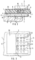
- Fig. 1 and Fig. 2 each show a cross section through a first embodiment of the cooling device according to the invention.
- a double copper-clad circuit board 1 made of insulating material has on its top 6 next to those for Wiring of components required a first conductor tracks large-area metallization 8 on and on the underside 7 a second large-area metallization 9, both over a plurality of through-metallized bores 10, so-called Vias, galvanically and thermally conductive with each other are connected.
- On the first large-scale metallization 8 is a heat generating electronic power device 2 over the plated-through holes 10 in a known manner Way e.g. soldered directly in the reflow soldering process.
- the solder application can take place so that solder 20 at least partially in the through-plated holes 10 of the top 6 is filled out.
- the thermal plate is in the form of a tin-plated Copper plate formed, the thickness of which is preferably approximately between 0.5 and 1.5 mm should be. But it is also conceivable another good heat-conducting material for the heat-conducting plate to use. Deviating from that in FIGS. 1 to Fig. 3 illustrated embodiment can the heat conducting plate 3, for example, the shape of a simple cuboid Have plate, the floor plan with the through-metallized Bore-provided area of the printed circuit board 1 corresponds. For soldering the heat conducting plate to the circuit board is then the circuit board 3, for example with the Bottom 7 turned upwards.
- FIG. 1 to 3 is the thermal plate 3, however, in the wave soldering process soldered to the second metallization 9. Because on the bottom 7 of the circuit board 1 often further components are provided are with the wave soldering method with connections the underside should be soldered, this has the advantage that the soldering of the thermal plate 3 together with the soldering these components can be done.
- FIG. 1 to Fig. 3 embodiment shows the thermal plate 3 a cuboid basic form, in the two rectangular recesses 15 are provided, which by three fingers 3a are delimited by one not with recesses project area 3b laterally. The recesses 15 are through the thermal plate from the top 18 passed through to the bottom 19. Like on can best be seen in FIG.
- the heat-conducting plate 3 an E-shaped floor plan.
- the one with the recesses the heat-conducting plate can also have a different shape.
- the area provided with the recesses is the Thermal plate at least the size of the via holes 10 provided area of the circuit board.
- the thermal plate 3 can be as follows on the circuit board 1 can be attached. First, on the top 18 of the not provided with the recesses, to the left in Fig. 3 the dashed line 3b arranged an adhesive 17 applied and then the thermal plate 3 with her Top 18 on the metallization 9 on the bottom 7 glued on the circuit board. It is important to ensure that area 3b is not on the plated through holes 10 is glued and that the recesses 15th provided, shown in Fig. 3 to the right of the dashed line Area above the plated-through holes 15 is arranged.
- the adhesive layer 17 serves to hold the Thermal plate during subsequent wave soldering and becomes very applied thinly.
- the heat-conducting plate is through the adhesive layer 17 through a very narrow gap from the second Metallization 9 spaced.
- the solder mask can also be applied prior to bonding be applied to the thermal plate.
- the one with the thermal plate provided circuit board is then one Wave soldering station supplied.
- wave soldering prevents Solder mask a solder deposit on the not with the recesses 15 provided area 3b of the underside 19 of the heat-conducting plate, while on the bottom 19 in the area the finger deposits 3a solder.
- solder 20 continues to penetrate into the recesses 15 and in the narrow gap between the second metallization 9 and the top 18 of the thermal plate.
- the through-plated holes 10 fill up Solder.
- At least the through the recesses are preferred 15 accessible holes 10 completely with solder replenished. This forms solder bridges, which the Vias 10 with the inner wall 14 of the recesses 15 very good heat conducting connection.
- the solder mask is removed and one in its place electrically insulating and good heat-conducting layer 5 the area 3b not provided with the plated-through holes applied to the underside 19 of the heat-conducting plate.
- the heat sink 4 has a raised area, which serves as a support area serves for the insulating layer 5. Below the The heat sink 4 has a depression, so that it is ensured that the deposited on the fingers 3a Lot 20 cannot touch the heat sink.
- the insulation layer 5 can also be designed as an adhesive layer or adhesive film be and thus the mechanical bracket serve the circuit board on the heat sink.
Landscapes
- Engineering & Computer Science (AREA)
- Microelectronics & Electronic Packaging (AREA)
- Cooling Or The Like Of Electrical Apparatus (AREA)
- Structure Of Printed Boards (AREA)
- Cooling Or The Like Of Semiconductors Or Solid State Devices (AREA)
Applications Claiming Priority (2)
| Application Number | Priority Date | Filing Date | Title |
|---|---|---|---|
| DE19752797 | 1997-11-28 | ||
| DE19752797A DE19752797A1 (de) | 1997-11-28 | 1997-11-28 | Kühlvorrichtung für ein auf einer Leiterplatte angeordnetes, wärmeerzeugendes Bauelement |
Publications (3)
| Publication Number | Publication Date |
|---|---|
| EP0920055A2 true EP0920055A2 (fr) | 1999-06-02 |
| EP0920055A3 EP0920055A3 (fr) | 1999-07-28 |
| EP0920055B1 EP0920055B1 (fr) | 2005-11-30 |
Family
ID=7850109
Family Applications (1)
| Application Number | Title | Priority Date | Filing Date |
|---|---|---|---|
| EP98115694A Expired - Lifetime EP0920055B1 (fr) | 1997-11-28 | 1998-08-20 | Dispositif de refroidissement pour un composant générant de la chaleur sur un circuit imprimé |
Country Status (3)
| Country | Link |
|---|---|
| EP (1) | EP0920055B1 (fr) |
| JP (1) | JP4469429B2 (fr) |
| DE (2) | DE19752797A1 (fr) |
Cited By (21)
| Publication number | Priority date | Publication date | Assignee | Title |
|---|---|---|---|---|
| WO2001006821A1 (fr) * | 1999-07-15 | 2001-01-25 | Incep Technologies, Inc. | Boitier encapsule entre deux cartes a circuit imprime |
| US6356448B1 (en) | 1999-11-02 | 2002-03-12 | Inceptechnologies, Inc. | Inter-circuit encapsulated packaging for power delivery |
| FR2819372A1 (fr) * | 2001-01-09 | 2002-07-12 | Deere & Co | Carte de circuit imprime a evaluation de chaleur |
| US6452113B2 (en) | 1999-07-15 | 2002-09-17 | Incep Technologies, Inc. | Apparatus for providing power to a microprocessor with integrated thermal and EMI management |
| WO2003019997A1 (fr) * | 2001-08-22 | 2003-03-06 | Vanner, Inc. | Dissipateur thermique ameliore pour dispositifs d'alimentation montes en surface |
| US6618268B2 (en) | 1999-07-15 | 2003-09-09 | Incep Technologies, Inc. | Apparatus for delivering power to high performance electronic assemblies |
| US6623279B2 (en) | 1999-07-15 | 2003-09-23 | Incep Technologies, Inc. | Separable power delivery connector |
| US6741480B2 (en) | 1999-07-15 | 2004-05-25 | Incep Technologies, Inc. | Integrated power delivery with flex circuit interconnection for high density power circuits for integrated circuits and systems |
| US6801431B2 (en) | 1999-07-15 | 2004-10-05 | Incep Technologies, Inc. | Integrated power delivery and cooling system for high power microprocessors |
| US6847529B2 (en) | 1999-07-15 | 2005-01-25 | Incep Technologies, Inc. | Ultra-low impedance power interconnection system for electronic packages |
| US6947293B2 (en) | 1999-07-15 | 2005-09-20 | Incep Technologies | Method and apparatus for providing power to a microprocessor with integrated thermal and EMI management |
| EP1603376A1 (fr) * | 2004-06-03 | 2005-12-07 | BREE (Beauce Réalisations et Études Électroniques) | Circuit imprimé à dépôt sélectif |
| US7167379B2 (en) | 2001-02-16 | 2007-01-23 | Dibene Ii Joseph T | Micro-spring interconnect systems for low impedance high power applications |
| EP1903839A2 (fr) | 2006-09-20 | 2008-03-26 | Sumitomo Wiring Systems, Ltd. | Procédé de production de carte de circuit imprimé avec structure à rayonnement thermique et panneau de circuit imprimé avec structure à rayonnement thermique |
| WO2010012271A3 (fr) * | 2008-07-30 | 2010-05-06 | Brose Fahrzeugteile Gmbh & Co. Kg, Würzburg | Dispositif, en particulier pour la conduction de courant, et procédé de fabrication d'un dispositif, en particulier pour la conduction de courant |
| US7881072B2 (en) | 1999-07-15 | 2011-02-01 | Molex Incorporated | System and method for processor power delivery and thermal management |
| EP2388812A2 (fr) * | 2010-05-17 | 2011-11-23 | Sunonwealth Electric Machine Industry Co., Ltd. | Ensemble de dissipation de chaleur |
| US8794797B2 (en) | 2003-11-07 | 2014-08-05 | Teknoware Oy | Hybrid illuminator |
| ITMI20130520A1 (it) * | 2013-04-05 | 2014-10-06 | St Microelectronics Srl | Realizzazione di un dissipatore di calore tramite saldatura ad onda |
| EP3203513A1 (fr) * | 2016-02-05 | 2017-08-09 | Robert Bosch GmbH | Système de contact comprenant un porte-circuit et élément structurel |
| WO2018158061A1 (fr) * | 2017-03-02 | 2018-09-07 | HELLA GmbH & Co. KGaA | Procédé de fabrication d'un module électrique |
Families Citing this family (21)
| Publication number | Priority date | Publication date | Assignee | Title |
|---|---|---|---|---|
| DE10033352B4 (de) * | 2000-07-08 | 2010-08-19 | Robert Bosch Gmbh | Verfahren zur Herstellung einer elektronischen Baugruppe und elektronische Baugruppe |
| KR20020074073A (ko) * | 2001-03-16 | 2002-09-28 | 엘지전자 주식회사 | 아이씨 방열구조 |
| JP2003289191A (ja) | 2002-03-28 | 2003-10-10 | Denso Corp | 電子制御装置 |
| DE10343429B4 (de) * | 2002-10-14 | 2007-08-16 | Heidelberger Druckmaschinen Ag | Anordnung zum Kühlen eines auf einer Leiterplatte angeordneten elektrischen Bauelementes |
| DE10335805A1 (de) * | 2003-08-05 | 2005-03-17 | Schweizer Electronic Ag | Leiterplatte und Verfahren zu ihrer Herstellung |
| JP4461268B2 (ja) * | 2004-03-30 | 2010-05-12 | Dowaメタルテック株式会社 | 半導体装置部品およびその製造方法ならびにこれを用いた半導体装置 |
| JP2007036172A (ja) * | 2005-11-28 | 2007-02-08 | Shin Kobe Electric Mach Co Ltd | 積層回路基板 |
| DE102006004320A1 (de) * | 2006-01-31 | 2007-08-09 | Häusermann GmbH | Leiterplatte mit funktionalen Elementen und selektiv gefüllten und thermisch leitfähigen Durchsteigelöchern sowie Herstellverfahren und Anwendung |
| JP4992532B2 (ja) * | 2006-04-27 | 2012-08-08 | パナソニック株式会社 | 放熱基板及びその製造方法 |
| US7410297B2 (en) | 2006-08-18 | 2008-08-12 | General Electric Company | Apparatus for controlling radiation in a radiation generator |
| DE102007039800B3 (de) * | 2007-08-23 | 2008-12-11 | Festo Ag & Co. Kg | Kühlanordnung und damit ausgestattetes elektronisches Gerät |
| DE102007044358A1 (de) | 2007-09-17 | 2009-03-19 | Robert Bosch Gmbh | Vorrichtung zum Kühlen von elektronischen Bauteilen |
| DE102007057533B4 (de) * | 2007-11-29 | 2016-07-07 | Fraunhofer-Gesellschaft zur Förderung der angewandten Forschung e.V. | Kühlkörper, Verfahren zur Herstellung eines Kühlkörpers und Leiterplatte mit Kühlkörper |
| DE102008019797B4 (de) * | 2008-04-18 | 2023-09-21 | Sew-Eurodrive Gmbh & Co Kg | Kühlanordnung und Umrichter |
| JP6618549B2 (ja) | 2015-12-03 | 2019-12-11 | 三菱電機株式会社 | 半導体装置 |
| DE102016220833A1 (de) | 2016-10-24 | 2018-04-26 | Robert Bosch Gmbh | Steuergerät mit wärmeleitend an das Gehäuse angebundenem elektronischem Bauelement |
| DE112018002707B4 (de) | 2017-05-26 | 2022-05-05 | Mitsubishi Electric Corporation | Halbleiterbauelement |
| CN107191795A (zh) * | 2017-06-06 | 2017-09-22 | 安徽艳阳电气集团有限公司 | 一种基于高散热性能的led灯具 |
| DE112018006370B4 (de) | 2017-12-14 | 2024-09-19 | Mitsubishi Electric Corporation | Halbleitereinrichtung |
| DE102018109920A1 (de) * | 2018-04-25 | 2019-10-31 | Dr. Ing. H.C. F. Porsche Aktiengesellschaft | Kühlung von leistungselektronischen Schaltungen |
| EP3588524B1 (fr) * | 2018-06-28 | 2020-08-05 | Black & Decker Inc. | Module de commutateur électronique doté d'une diode de retour intégrée |
Family Cites Families (6)
| Publication number | Priority date | Publication date | Assignee | Title |
|---|---|---|---|---|
| US5014904A (en) * | 1990-01-16 | 1991-05-14 | Cray Research, Inc. | Board-mounted thermal path connector and cold plate |
| DE4107312A1 (de) * | 1991-03-07 | 1992-09-10 | Telefunken Electronic Gmbh | Montageanordnung von halbleiterbauelementen auf einer leiterplatte |
| DE4232575A1 (de) * | 1992-09-29 | 1994-03-31 | Bosch Gmbh Robert | Anordnung mit einer Leiterplatte, mindestens einem Leistungsbauelement und einem Kühlkörper |
| FR2706730B1 (fr) * | 1993-06-18 | 1995-08-25 | Sagem | Module électronique de puissance ayant un support d'évacuation de la chaleur. |
| DE69401040T2 (de) * | 1993-07-12 | 1997-06-05 | Nippon Electric Co | Gehäusestruktur für Mikrowellenschaltung |
| DE19506664A1 (de) * | 1995-02-25 | 1996-02-29 | Bosch Gmbh Robert | Elektrisches Gerät |
-
1997
- 1997-11-28 DE DE19752797A patent/DE19752797A1/de not_active Ceased
-
1998
- 1998-08-20 DE DE59813241T patent/DE59813241D1/de not_active Expired - Lifetime
- 1998-08-20 EP EP98115694A patent/EP0920055B1/fr not_active Expired - Lifetime
- 1998-11-27 JP JP33755198A patent/JP4469429B2/ja not_active Expired - Lifetime
Cited By (30)
| Publication number | Priority date | Publication date | Assignee | Title |
|---|---|---|---|---|
| US7881072B2 (en) | 1999-07-15 | 2011-02-01 | Molex Incorporated | System and method for processor power delivery and thermal management |
| US7245507B2 (en) | 1999-07-15 | 2007-07-17 | Dibene Ii Joseph T | Method and apparatus for providing power to a microprocessor with integrated thermal and EMI management |
| WO2001006821A1 (fr) * | 1999-07-15 | 2001-01-25 | Incep Technologies, Inc. | Boitier encapsule entre deux cartes a circuit imprime |
| US6304450B1 (en) | 1999-07-15 | 2001-10-16 | Incep Technologies, Inc. | Inter-circuit encapsulated packaging |
| US6452113B2 (en) | 1999-07-15 | 2002-09-17 | Incep Technologies, Inc. | Apparatus for providing power to a microprocessor with integrated thermal and EMI management |
| US6947293B2 (en) | 1999-07-15 | 2005-09-20 | Incep Technologies | Method and apparatus for providing power to a microprocessor with integrated thermal and EMI management |
| US6847529B2 (en) | 1999-07-15 | 2005-01-25 | Incep Technologies, Inc. | Ultra-low impedance power interconnection system for electronic packages |
| US6618268B2 (en) | 1999-07-15 | 2003-09-09 | Incep Technologies, Inc. | Apparatus for delivering power to high performance electronic assemblies |
| US6623279B2 (en) | 1999-07-15 | 2003-09-23 | Incep Technologies, Inc. | Separable power delivery connector |
| US6801431B2 (en) | 1999-07-15 | 2004-10-05 | Incep Technologies, Inc. | Integrated power delivery and cooling system for high power microprocessors |
| US6741480B2 (en) | 1999-07-15 | 2004-05-25 | Incep Technologies, Inc. | Integrated power delivery with flex circuit interconnection for high density power circuits for integrated circuits and systems |
| US6356448B1 (en) | 1999-11-02 | 2002-03-12 | Inceptechnologies, Inc. | Inter-circuit encapsulated packaging for power delivery |
| GB2375655B (en) * | 2001-01-09 | 2004-03-10 | Deere & Co | Circuit board assembly |
| GB2375655A (en) * | 2001-01-09 | 2002-11-20 | Deere & Co | Circuit board assembly |
| FR2819372A1 (fr) * | 2001-01-09 | 2002-07-12 | Deere & Co | Carte de circuit imprime a evaluation de chaleur |
| US7167379B2 (en) | 2001-02-16 | 2007-01-23 | Dibene Ii Joseph T | Micro-spring interconnect systems for low impedance high power applications |
| WO2003019997A1 (fr) * | 2001-08-22 | 2003-03-06 | Vanner, Inc. | Dissipateur thermique ameliore pour dispositifs d'alimentation montes en surface |
| US8794797B2 (en) | 2003-11-07 | 2014-08-05 | Teknoware Oy | Hybrid illuminator |
| EP1603376A1 (fr) * | 2004-06-03 | 2005-12-07 | BREE (Beauce Réalisations et Études Électroniques) | Circuit imprimé à dépôt sélectif |
| US7606038B2 (en) | 2006-09-20 | 2009-10-20 | Sumitomo Wiring Systems, Ltd. | Method for producing a printed circuit board with a heat radiating structure and a printed circuit board with a heat radiating structure |
| EP1903839A2 (fr) | 2006-09-20 | 2008-03-26 | Sumitomo Wiring Systems, Ltd. | Procédé de production de carte de circuit imprimé avec structure à rayonnement thermique et panneau de circuit imprimé avec structure à rayonnement thermique |
| EP1903839A3 (fr) * | 2006-09-20 | 2009-05-27 | Sumitomo Wiring Systems, Ltd. | Procédé de production de carte de circuit imprimé avec structure à rayonnement thermique et panneau de circuit imprimé avec structure à rayonnement thermique |
| WO2010012271A3 (fr) * | 2008-07-30 | 2010-05-06 | Brose Fahrzeugteile Gmbh & Co. Kg, Würzburg | Dispositif, en particulier pour la conduction de courant, et procédé de fabrication d'un dispositif, en particulier pour la conduction de courant |
| EP2388812A2 (fr) * | 2010-05-17 | 2011-11-23 | Sunonwealth Electric Machine Industry Co., Ltd. | Ensemble de dissipation de chaleur |
| ITMI20130520A1 (it) * | 2013-04-05 | 2014-10-06 | St Microelectronics Srl | Realizzazione di un dissipatore di calore tramite saldatura ad onda |
| US9237644B2 (en) | 2013-04-05 | 2016-01-12 | Stmicroelectronics S.R.L. | Manufacturing of a heat sink by wave soldering |
| US9615444B2 (en) | 2013-04-05 | 2017-04-04 | Stmicroelectronics S.R.L. | Manufacturing of a heat sink by wave soldering |
| EP3203513A1 (fr) * | 2016-02-05 | 2017-08-09 | Robert Bosch GmbH | Système de contact comprenant un porte-circuit et élément structurel |
| WO2018158061A1 (fr) * | 2017-03-02 | 2018-09-07 | HELLA GmbH & Co. KGaA | Procédé de fabrication d'un module électrique |
| CN110352632A (zh) * | 2017-03-02 | 2019-10-18 | 黑拉有限责任两合公司 | 用于制造电气组件的方法 |
Also Published As
| Publication number | Publication date |
|---|---|
| DE59813241D1 (de) | 2006-01-05 |
| EP0920055A3 (fr) | 1999-07-28 |
| EP0920055B1 (fr) | 2005-11-30 |
| DE19752797A1 (de) | 1999-06-10 |
| JPH11345921A (ja) | 1999-12-14 |
| JP4469429B2 (ja) | 2010-05-26 |
Similar Documents
| Publication | Publication Date | Title |
|---|---|---|
| EP0920055B1 (fr) | Dispositif de refroidissement pour un composant générant de la chaleur sur un circuit imprimé | |
| EP0934687B1 (fr) | Ensemble comprenant un substrat pour des composants de puissance et un element de refroidissement, et procede pour produire ledit ensemble | |
| DE102011083223B4 (de) | Leistungshalbleitermodul mit integrierter Dickschichtleiterplatte | |
| DE69615038T2 (de) | Verfahren zur oberflächenmontage eines kühlkörpers auf einer leiterplatte | |
| EP2043412B1 (fr) | Rails conducteurs dotés d'une dissipation de chaleur | |
| DE112016005794B4 (de) | Schaltungsanordnung und elektrischer Anschlusskasten | |
| DE19634202C2 (de) | Halbleitervorrichtung | |
| DE4326506A1 (de) | Elektrisches Gerät, insbesondere Schalt- oder Steuergerät für Kraftfahrzeuge | |
| DE19928788A1 (de) | Elektronische Keramikkomponente | |
| DE102004021054B4 (de) | Halbleiterbauelement und Verfahren zu seiner Herstellung | |
| EP3095307B1 (fr) | Circuit imprimé, montage et procédé de fabrication d'un montage | |
| DE19509441A1 (de) | Hybrid-integrierte Leistungsschaltungsvorrichtung | |
| DE4335946C2 (de) | Anordnung bestehend aus einer Leiterplatte | |
| DE69904750T2 (de) | Elektrisches bauteil und elektrischer schaltungsmodul mit verbundenen erdungsflächen | |
| EP1445799A2 (fr) | Dispositif à dissipation de chaleur pour un semi-conducteur sur un circuit imprimé | |
| EP1503615A2 (fr) | Panneau à circuit avec un composant refroidi, en particulier un composant CMS | |
| EP0881866A1 (fr) | Dispositif de commande | |
| EP1929847B1 (fr) | Carte de circuits imprimes | |
| DE202014006215U1 (de) | Leiterplatte mit gekühltem Baustein, insbesondere SMD-Baustein | |
| EP0938252A2 (fr) | Agencement de circuit électrique | |
| EP0849981B1 (fr) | Panneau à circuit à double face ou multicouche laminé d'un film en cuivre et méthode de fabrication associé | |
| DE19805492C2 (de) | Leiterplatte | |
| DE10064221B4 (de) | Leiterplatine mit gekühltem SMD-Baustein | |
| DE10217214B4 (de) | Kühlanordnung für eine Schaltungsanordnung | |
| EP0651598B1 (fr) | Module de circuit électronique |
Legal Events
| Date | Code | Title | Description |
|---|---|---|---|
| PUAI | Public reference made under article 153(3) epc to a published international application that has entered the european phase |
Free format text: ORIGINAL CODE: 0009012 |
|
| AK | Designated contracting states |
Kind code of ref document: A2 Designated state(s): DE FR GB IT |
|
| AX | Request for extension of the european patent |
Free format text: AL;LT;LV;MK;RO;SI |
|
| PUAL | Search report despatched |
Free format text: ORIGINAL CODE: 0009013 |
|
| AK | Designated contracting states |
Kind code of ref document: A3 Designated state(s): AT BE CH CY DE DK ES FI FR GB GR IE IT LI LU MC NL PT SE |
|
| AX | Request for extension of the european patent |
Free format text: AL;LT;LV;MK;RO;SI |
|
| RIC1 | Information provided on ipc code assigned before grant |
Free format text: 6H 05K 1/02 A, 6H 05K 7/20 B |
|
| 17P | Request for examination filed |
Effective date: 20000128 |
|
| AKX | Designation fees paid |
Free format text: DE FR GB IT |
|
| 17Q | First examination report despatched |
Effective date: 20041012 |
|
| GRAP | Despatch of communication of intention to grant a patent |
Free format text: ORIGINAL CODE: EPIDOSNIGR1 |
|
| RTI1 | Title (correction) |
Free format text: COOLING DEVICE FOR A HEAT GENERATING COMPONENT ON A PRINTED BOARD |
|
| GRAS | Grant fee paid |
Free format text: ORIGINAL CODE: EPIDOSNIGR3 |
|
| GRAA | (expected) grant |
Free format text: ORIGINAL CODE: 0009210 |
|
| AK | Designated contracting states |
Kind code of ref document: B1 Designated state(s): DE FR GB IT |
|
| PG25 | Lapsed in a contracting state [announced via postgrant information from national office to epo] |
Ref country code: GB Free format text: LAPSE BECAUSE OF FAILURE TO SUBMIT A TRANSLATION OF THE DESCRIPTION OR TO PAY THE FEE WITHIN THE PRESCRIBED TIME-LIMIT Effective date: 20051130 |
|
| REG | Reference to a national code |
Ref country code: GB Ref legal event code: FG4D Free format text: NOT ENGLISH |
|
| REF | Corresponds to: |
Ref document number: 59813241 Country of ref document: DE Date of ref document: 20060105 Kind code of ref document: P |
|
| GBV | Gb: ep patent (uk) treated as always having been void in accordance with gb section 77(7)/1977 [no translation filed] |
Effective date: 20051130 |
|
| ET | Fr: translation filed | ||
| PLBE | No opposition filed within time limit |
Free format text: ORIGINAL CODE: 0009261 |
|
| STAA | Information on the status of an ep patent application or granted ep patent |
Free format text: STATUS: NO OPPOSITION FILED WITHIN TIME LIMIT |
|
| 26N | No opposition filed |
Effective date: 20060831 |
|
| PGFP | Annual fee paid to national office [announced via postgrant information from national office to epo] |
Ref country code: FR Payment date: 20090819 Year of fee payment: 12 |
|
| PGFP | Annual fee paid to national office [announced via postgrant information from national office to epo] |
Ref country code: DE Payment date: 20091026 Year of fee payment: 12 |
|
| PGFP | Annual fee paid to national office [announced via postgrant information from national office to epo] |
Ref country code: IT Payment date: 20090824 Year of fee payment: 12 |
|
| REG | Reference to a national code |
Ref country code: FR Ref legal event code: ST Effective date: 20110502 |
|
| PG25 | Lapsed in a contracting state [announced via postgrant information from national office to epo] |
Ref country code: IT Free format text: LAPSE BECAUSE OF NON-PAYMENT OF DUE FEES Effective date: 20100820 |
|
| REG | Reference to a national code |
Ref country code: DE Ref legal event code: R119 Ref document number: 59813241 Country of ref document: DE Effective date: 20110301 |
|
| PG25 | Lapsed in a contracting state [announced via postgrant information from national office to epo] |
Ref country code: DE Free format text: LAPSE BECAUSE OF NON-PAYMENT OF DUE FEES Effective date: 20110301 Ref country code: FR Free format text: LAPSE BECAUSE OF NON-PAYMENT OF DUE FEES Effective date: 20100831 |