EP0920096A2 - Laser à semi-conducteur - Google Patents
Laser à semi-conducteur Download PDFInfo
- Publication number
- EP0920096A2 EP0920096A2 EP98122308A EP98122308A EP0920096A2 EP 0920096 A2 EP0920096 A2 EP 0920096A2 EP 98122308 A EP98122308 A EP 98122308A EP 98122308 A EP98122308 A EP 98122308A EP 0920096 A2 EP0920096 A2 EP 0920096A2
- Authority
- EP
- European Patent Office
- Prior art keywords
- layer
- semiconductor laser
- optical waveguide
- substrate
- gaas substrate
- Prior art date
- Legal status (The legal status is an assumption and is not a legal conclusion. Google has not performed a legal analysis and makes no representation as to the accuracy of the status listed.)
- Granted
Links
Images






Classifications
-
- H—ELECTRICITY
- H01—ELECTRIC ELEMENTS
- H01S—DEVICES USING THE PROCESS OF LIGHT AMPLIFICATION BY STIMULATED EMISSION OF RADIATION [LASER] TO AMPLIFY OR GENERATE LIGHT; DEVICES USING STIMULATED EMISSION OF ELECTROMAGNETIC RADIATION IN WAVE RANGES OTHER THAN OPTICAL
- H01S5/00—Semiconductor lasers
- H01S5/30—Structure or shape of the active region; Materials used for the active region
- H01S5/34—Structure or shape of the active region; Materials used for the active region comprising quantum well or superlattice structures, e.g. single quantum well [SQW] lasers, multiple quantum well [MQW] lasers or graded index separate confinement heterostructure [GRINSCH] lasers
- H01S5/343—Structure or shape of the active region; Materials used for the active region comprising quantum well or superlattice structures, e.g. single quantum well [SQW] lasers, multiple quantum well [MQW] lasers or graded index separate confinement heterostructure [GRINSCH] lasers in AIIIBV compounds, e.g. AlGaAs-laser, InP-based laser
- H01S5/34313—Structure or shape of the active region; Materials used for the active region comprising quantum well or superlattice structures, e.g. single quantum well [SQW] lasers, multiple quantum well [MQW] lasers or graded index separate confinement heterostructure [GRINSCH] lasers in AIIIBV compounds, e.g. AlGaAs-laser, InP-based laser with a well layer having only As as V-compound, e.g. AlGaAs, InGaAs
-
- B—PERFORMING OPERATIONS; TRANSPORTING
- B82—NANOTECHNOLOGY
- B82Y—SPECIFIC USES OR APPLICATIONS OF NANOSTRUCTURES; MEASUREMENT OR ANALYSIS OF NANOSTRUCTURES; MANUFACTURE OR TREATMENT OF NANOSTRUCTURES
- B82Y20/00—Nanooptics, e.g. quantum optics or photonic crystals
-
- H—ELECTRICITY
- H01—ELECTRIC ELEMENTS
- H01S—DEVICES USING THE PROCESS OF LIGHT AMPLIFICATION BY STIMULATED EMISSION OF RADIATION [LASER] TO AMPLIFY OR GENERATE LIGHT; DEVICES USING STIMULATED EMISSION OF ELECTROMAGNETIC RADIATION IN WAVE RANGES OTHER THAN OPTICAL
- H01S5/00—Semiconductor lasers
- H01S5/30—Structure or shape of the active region; Materials used for the active region
- H01S5/34—Structure or shape of the active region; Materials used for the active region comprising quantum well or superlattice structures, e.g. single quantum well [SQW] lasers, multiple quantum well [MQW] lasers or graded index separate confinement heterostructure [GRINSCH] lasers
- H01S5/343—Structure or shape of the active region; Materials used for the active region comprising quantum well or superlattice structures, e.g. single quantum well [SQW] lasers, multiple quantum well [MQW] lasers or graded index separate confinement heterostructure [GRINSCH] lasers in AIIIBV compounds, e.g. AlGaAs-laser, InP-based laser
-
- H—ELECTRICITY
- H01—ELECTRIC ELEMENTS
- H01S—DEVICES USING THE PROCESS OF LIGHT AMPLIFICATION BY STIMULATED EMISSION OF RADIATION [LASER] TO AMPLIFY OR GENERATE LIGHT; DEVICES USING STIMULATED EMISSION OF ELECTROMAGNETIC RADIATION IN WAVE RANGES OTHER THAN OPTICAL
- H01S5/00—Semiconductor lasers
- H01S5/20—Structure or shape of the semiconductor body to guide the optical wave ; Confining structures perpendicular to the optical axis, e.g. index or gain guiding, stripe geometry, broad area lasers, gain tailoring, transverse or lateral reflectors, special cladding structures, MQW barrier reflection layers
- H01S5/2004—Confining in the direction perpendicular to the layer structure
- H01S5/2009—Confining in the direction perpendicular to the layer structure by using electron barrier layers
-
- H—ELECTRICITY
- H01—ELECTRIC ELEMENTS
- H01S—DEVICES USING THE PROCESS OF LIGHT AMPLIFICATION BY STIMULATED EMISSION OF RADIATION [LASER] TO AMPLIFY OR GENERATE LIGHT; DEVICES USING STIMULATED EMISSION OF ELECTROMAGNETIC RADIATION IN WAVE RANGES OTHER THAN OPTICAL
- H01S5/00—Semiconductor lasers
- H01S5/30—Structure or shape of the active region; Materials used for the active region
- H01S5/32—Structure or shape of the active region; Materials used for the active region comprising PN junctions, e.g. hetero- or double- heterostructures
- H01S5/323—Structure or shape of the active region; Materials used for the active region comprising PN junctions, e.g. hetero- or double- heterostructures in AIIIBV compounds, e.g. AlGaAs-laser, InP-based laser
- H01S5/32308—Structure or shape of the active region; Materials used for the active region comprising PN junctions, e.g. hetero- or double- heterostructures in AIIIBV compounds, e.g. AlGaAs-laser, InP-based laser emitting light at a wavelength less than 900 nm
- H01S5/32333—Structure or shape of the active region; Materials used for the active region comprising PN junctions, e.g. hetero- or double- heterostructures in AIIIBV compounds, e.g. AlGaAs-laser, InP-based laser emitting light at a wavelength less than 900 nm based on InGaAsP
-
- H—ELECTRICITY
- H01—ELECTRIC ELEMENTS
- H01S—DEVICES USING THE PROCESS OF LIGHT AMPLIFICATION BY STIMULATED EMISSION OF RADIATION [LASER] TO AMPLIFY OR GENERATE LIGHT; DEVICES USING STIMULATED EMISSION OF ELECTROMAGNETIC RADIATION IN WAVE RANGES OTHER THAN OPTICAL
- H01S5/00—Semiconductor lasers
- H01S5/30—Structure or shape of the active region; Materials used for the active region
- H01S5/34—Structure or shape of the active region; Materials used for the active region comprising quantum well or superlattice structures, e.g. single quantum well [SQW] lasers, multiple quantum well [MQW] lasers or graded index separate confinement heterostructure [GRINSCH] lasers
- H01S5/3403—Structure or shape of the active region; Materials used for the active region comprising quantum well or superlattice structures, e.g. single quantum well [SQW] lasers, multiple quantum well [MQW] lasers or graded index separate confinement heterostructure [GRINSCH] lasers having a strained layer structure in which the strain performs a special function, e.g. general strain effects, strain versus polarisation
Definitions
- This invention relates to a semiconductor laser device.
- This invention particularly relates to a composition of a semiconductor layer, which constitutes a semiconductor laser device.
- a semiconductor laser which produces a laser beam having a wavelength in the band of 0.7 ⁇ m to 0.85 ⁇ m
- a semiconductor laser comprising an n-GaAs substrate, an n-AlGaAs cladding layer, an n- or i-AlGaAs optical waveguide layer, an i-AlGaAs active layer, a p- or i-AlGaAs optical waveguide layer, a p-AlGaAs cladding layer, and a p-GaAs capping layer, which layers are formed on the substrate.
- a semiconductor laser which produces a laser beam having a wavelength of a 875nm band and is of the all Al-free type
- a semiconductor laser comprising an n-GaAs substrate, an n-InGaP cladding layer, an undoped InGaAsP optical waveguide layer, a GaAs quantum well active layer, an undoped InGaAsP optical waveguide layer, a p-InGaP cladding layer, and a p-GaAs capping layer, which layers are formed on the substrate.
- Such a semiconductor laser is described in, for example, "IEEE Photonics Technology Letters," Vol. 6, No. 4, 1994, p. 465.
- the proposed Al-free semiconductor laser has the drawbacks in that the dependence of device characteristics upon temperatures is large and in that, though the maximum light output power is as high as 4.2W, the light emission efficiency becomes low due to the occurrence of leak current at light output power of above 1W.
- the proposed Al-free semiconductor laser is not suitable as a high-output-power semiconductor laser for producing a laser beam having wavelengths of a short-wavelength band in the vicinity of 0.8 ⁇ m.
- a semiconductor laser which produces a laser beam having a wavelength of a 0.8 ⁇ m band and in which an active layer is of the Al-free type
- a semiconductor laser comprising an n-GaAs substrate, an n-AlGaAs cladding layer, an i-InGaP optical waveguide layer, an InGaAsP quantum well active layer, an i-InGaP optical waveguide layer, a p-AlGaAs cladding layer, and a p-GaAs capping layer, which layers are formed on the substrate.
- Such a semiconductor laser is described in, for example, "Jpn. J. Appl. Phys.,"Vol. 34, 1995, pp.
- the reported semiconductor laser has the drawbacks in that the temperature characteristics of the device characteristics are high due to carrier overflow. Therefore, the drive current cannot be kept small under the conditions for radiation a laser beam having a high intensity, and the reliability cannot be kept high due to an increase in the device temperature due to heat generation.
- a semiconductor laser having an enhanced reliability has been proposed in, for example, "IEEE Journal of selected Topics in Quantum Electronics," Vol. 3, No. 2, 1997, p. 180.
- a GaInP semiconductor of a composition ratio having a compressive strain with respect to a substrate is employed as an active layer, and an AlGaInP layer having a tensile strain of at least a level that cancels the compressive strain of the active layer is employed as a side barrier layer. Crystal structure relaxation is caused to occur in the vicinity of a radiating end face of the laser device, and the band gap at the end face is kept large.
- the primary object of the present invention is to provide a semiconductor laser device for producing a laser beam having a wavelength of a 0.8 ⁇ m band, which device has a high durability and has a high reliability under conditions for radiating a laser beam having a high intensity.
- the present invention provides a first semiconductor laser device, comprising: a GaAs substrate, a first cladding layer, which has either one of p-type electrical conductivity and n-type electrical conductivity, a first optical waveguide layer, an In x2 Ga 1-x2 As 1-y2 P y2 first barrier layer, an In x3 Ga 1-x3 As 1-y3 P y3 quantum well active layer, an In x2 Ga 1-x2 As 1-y2 P y2 second barrier layer, a second optical waveguide layer, and a second cladding layer, which has the other electrical conductivity, the layers being overlaid in this order on the GaAs substrate, wherein each of the first cladding layer and the second cladding layer has a composition, which is lattice matched with the GaAs substrate,
- the present invention also provides a second semiconductor laser device, which is constituted in the same manner as that in the first semiconductor laser device, except that each of the first barrier layer and the second barrier layer has an In x2 Ga 1-x2 P type of composition.
- total layer thickness means the sum of the layer thickness of the first barrier layer and the layer thickness of the second barrier layer.
- the strain quantity of the tensile strain of each of the first and second barrier layers with respect to the GaAs substrate may be represented by the formula shown below.
- ⁇ 1 (a GaAs -a 1 )/a GaAs wherein ⁇ 1 represents the strain quantity, a GaAs represents the lattice constant of the GaAs substrate, and a 1 represents the lattice constant of the barrier layer.
- the strain quantity of the tensile strain of the quantum well active layer with respect to the GaAs substrate may be represented by the formula shown below.
- ⁇ 2 (a GaAs -a 2 )/a GaAs wherein ⁇ 2 represents the strain quantity, a GaAs represents the lattice constant of the GaAs substrate, and a 2 represents the lattice constant of the active layer.
- the strain quantity ⁇ 2 falls within the range of -0.0025 ⁇ ⁇ 2 ⁇ 0.0025.
- the composition of the quantum well active layer is selected from the group consisting of a composition, which is lattice matched with the GaAs substrate, and a composition, which has a tensile strain of at most 0.003 with respect to the GaAs substrate.
- the composition of the quantum well active layer is selected from compositions, which satisfy the condition of -0.0025 ⁇ 2 ⁇ 0.003.
- the first and second semiconductor laser devices in accordance with the present invention is constituted of a composition, in which the active layer does not contain Al. Therefore, the first and second semiconductor laser devices in accordance with the present invention have a higher durability than the conventional semiconductor laser for producing a laser beam having a wavelength of the 0.8 ⁇ m band. Also, with the first and second semiconductor laser devices in accordance with the present invention, which are provided with the InGaAsP or InGaP tensile strained barrier layers, lattice relaxation occurs in the vicinity of the active layer. By virtue of the lattice relaxation, the band gap can be kept large, and light absorption at a light radiating end face of the device can be reduced.
- the barrier height between the active layer and each barrier layer is kept large by the InGaAsP or InGaP tensile strained barrier layers, leakage of electrons and positive holes from the active layer to the optical waveguide layers can be reduced. As a result, the drive current can be kept small, and heat generation at the end face of the device can be restricted. Therefore, the reliability of the device under the conditions for radiation a laser beam having a high intensity can be enhanced.
- Figure 1 is a sectional view showing a first embodiment of the semiconductor laser device in accordance with the present invention. The constitution of the semiconductor laser device and how it is produced will be described hereinbelow.
- an n-Ga 1-z1 Al z1 As cladding layer 2 an n- or i-In x1 Ga 1-x1 As 1-y1 P y1 optical waveguide layer 3, an i-In x2 Ga 1-x2 As 1-y2 P y2 tensile strained barrier layer 4, an In x3 G 1-x3 As 1-y3 P y3 quantum well active layer 5, an i-In x2 G 1-x2 As 1-y2 P y2 tensile strained barrier layer 6, a p- or i-In x1 G 1-x1 As 1-y1 P y1 optical waveguide layer 7, a p-Ga 1-z1 Al z1 As cladding layer 8, and a p-GaAs contact layer 9 are formed on an n-GaAs substrate 1 with a metalorganic chemical vapor deposition process.
- a p-side electrode 10 is formed on the contact layer 9, and an n-side electrode 11 is formed on the substrate 1.
- Each of the cladding layers 2 and 8 is of a composition ratio, which is lattice matched with the GaAs substrate 1.
- each of the optical waveguide layers 3 and 7 is of a composition ratio, which is lattice matched with the GaAs substrate 1.
- an InGaAlAsP type of semiconductor layer may be employed.
- the quantum well active layer 5 has a composition, which is lattice matched with the substrate 1. Also, each of the tensile strained barrier layers 4 and 6 is set such that the strain quantity with respect to the substrate 1 may be equal to 0.007 and such that the layer thickness may be equal to 5nm. Alternatively, the quantum well active layer 5 may be set such that it may have a tensile strain of a strain quantity of at most 0.003 with respect to the GaAs substrate 1. The quantum well active layer 5 may also have a multiple quantum well structure. However, the product of the tensile strain quantity of the active layer 5 and the total thickness (the total layer thickness) of the active layer 5 should be at most 0.1nm.
- the tensile strained barrier layers 4 and 6 may be set such that the total layer thickness of the two barrier layers 4 and 6 may fall within the range of 10nm to 30nm, and such that the product of the strain quantity of each barrier layer and the total layer thickness may fall within the range of 0.05nm to 0.2nm.
- the "o" mark indicates the dependence of a threshold current I th upon temperature in the semiconductor laser device in accordance with the present invention
- the "X” mark indicates the dependence of the threshold current I th upon temperature in the semiconductor laser device for comparison, which is not provided with the tensile strained barrier layers.
- T the dependence of the threshold current upon temperature in the device is low, and that the reliability under the conditions for radiating a laser beam having a high intensity is enhanced.
- the characteristic temperature of the semiconductor laser device in accordance with the present invention was 125K and was higher by approximately 15K than in the semiconductor laser device for comparison, which is not provided with the tensile strained barrier layers.
- the active layer 5 does not contain Al. Therefore, the semiconductor laser device in accordance with the present invention has a high durability. Also, with the first embodiment of the semiconductor laser devices in accordance with the present invention, in which the tensile strained barrier layers 4 and 6 are formed above and below the active layer 5, lattice relaxation occurs in the vicinity of the active layer 5. By virtue of the lattice relaxation, the band gap can be kept large, and therefore the light absorption at a light radiating end face of the device can be reduced.
- the semiconductor laser device for radiating a laser beam having a wavelength of the 0.8 ⁇ m band which device has a high reliability under the conditions for radiation a laser beam having a high intensity, can be obtained.
- the GaAs substrate 1 has the n-type electrical conductivity.
- a substrate having the p-type electrical conductivity may be employed, and the semiconductor laser may be constituted through the growth from the p-type semiconductor layer.
- the semiconductor laser device in accordance with the present invention may be constituted as a gain guiding type of stripe laser, in which an insulating film having a stripe current injection window is formed on the contact layer.
- the semiconductor layer constitution in the aforesaid embodiment of the semiconductor laser device may be employed for a semiconductor laser provided with a refractive index guiding mechanism, which is produced with ordinary photo-lithographic and dry etching techniques.
- the semiconductor layer constitution may also be employed for a semiconductor laser provided with a diffraction grating, an integrated optical circuit, and the like.
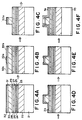
- Figures 4A, 4B, 4C, 4D, 4E, and 4F are sectional views showing how a second embodiment of the semiconductor laser device in accordance with the present invention is produced. The layer constitution of the second embodiment and how it is produced will be described hereinbelow.
- stripe portions 32b, 32b of the insulating film 32 are removed with an ordinary lithographic technique, such that the stripe portion 32a may not be removed.
- the remaining stripe portion 32a of the insulating film 32 is utilized as a mask, and the epitaxial layers ranging from the contact layer 31 to the upper surface of the etching blocking layer 29 are removed with a wet etching technique. In this manner, a ridge stripe is formed.
- the etching stops automatically at the etching blocking layer 29.
- the thickness of the upper first cladding layer 28 is adjusted such that the refractive index guiding in a fundamental transverse mode through the ridge stripe waveguide, which has been formed in the manner described above, can be achieved until a laser beam having a high intensity is radiated.
- the insulating film 32a is removed, and an insulating film 33 is formed over the entire areas of the surfaces of the ridge portion and the exposed etching blocking layer 29.
- the portion of the insulating film 33 at the top of the ridge stripe portion is then removed with an ordinary lithographic technique. Further, as illustrated in Figure 4F, a p-side electrode 34 is formed such that it may cover the exposed contact layer 31. Thereafter, the bottom surface of the substrate 21 is polished, and an n-side electrode 35 is formed on the bottom surface of the substrate 21.
- Figures 5A, 5B, 5C, 5D, 5E, and 5F are sectional views showing how a third embodiment of the semiconductor laser device in accordance with the present invention is produced. The layer constitution of the third embodiment and how it is produced will be described hereinbelow.
- an n-Ga 1-z1 Al z1 As cladding layer 42 an n- or i-In x1 Ga 1-x1 As 1-y1 P y1 optical waveguide layer 43, an i-In x2 Ga 1-x2 As 1-y2 P y2 tensile strained barrier layer 44, an In x3 Ga 1-x3 As 1-y3 P y3 quantum well active layer 45, an i-In x2 Ga 1-x2 As 1-y2 P y2 tensile strained barrier layer 46, a p- or i-In x1 Ga 1-x1 As 1-y1 P y1 optical waveguide layer 47, a p-In x4 (Ga 1-z4 Al z4 ) 1-x4 As 0.2 P 0.8 upper first cladding layer 48, a p-In x5 (Ga 1-z5 Al z5 ) 1-x5 P upper second cladding layer 49, and a p-GaAs contact layer 50
- stripe portions 52b, 52b of the insulating film 52 are removed with an ordinary lithographic technique, such that the stripe portion 52a may not be removed.
- the remaining stripe portion 52a of the insulating film 52 is utilized as a mask, and the epitaxial layers ranging from the contact layer 50 to the upper surface of the upper first cladding layer 48 are removed with a wet etching technique. In this manner, a ridge stripe is formed.
- the etching stops automatically at the upper first cladding layer 48.
- the thickness of the upper first cladding layer 48 is adjusted such that the refractive index guiding in a fundamental transverse mode through the ridge stripe waveguide, which has been formed in the manner described above, can be achieved until a laser beam having a high intensity is radiated.
- the insulating film 52a is removed, and an insulating film 53 is formed over the entire areas of the surfaces of the ridge portion and the exposed upper first cladding layer 48.
- the portion of the insulating film 53 at the top of the ridge stripe portion is then removed with an ordinary lithographic technique.
- a p-side electrode 54 is formed such that it may cover the exposed contact layer 50.
- the bottom surface of the substrate 41 is polished, and an n-side electrode 55 is formed on the bottom surface of the substrate 41.
- high-reflectivity coating is carried out on one of resonator surfaces, which have been formed by cleaving the sample, and low-reflectivity coating is carried out on the other resonator surface. Chip formation is then carried out. In this manner, the semiconductor laser device is formed. With the structure described above, a laser beam having a high intensity can be produced while the fundamental transverse mode is being kept.
- a refractive index guiding laser having an embedded structure can be produced by repeating the growth process three times by using the same etching stop mechanism as that described above.
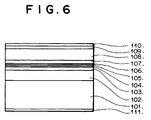
- Figure 6 is a sectional view showing a fourth embodiment of the semiconductor laser device in accordance with the present invention. The layer constitution of the fourth embodiment and how it is produced will be described hereinbelow.
- the quantum well active layer 105 has a composition, which is lattice matched with the GaAs substrate 101, or a composition, which has a tensile strain of a strain quantity of at most 0.003 with respect to the GaAs substrate 101.
- the quantum well active layer 105 may also have a multiple quantum well structure. However, the product of the tensile strain quantity of the active layer 105 and the total thickness (the total layer thickness) of the active layer 105 should be at most 0.1nm.
- the tensile strained barrier layers 104 and 106 are set such that the total layer thickness of the two barrier layers 104 and 106 may fall within the range of 10nm to 30nm, and such that the product of the strain quantity of each barrier layer and the total layer thickness may fall within the range of 0.05nm to 0.2nm.
- Each tensile strained barrier layer may be a ternary In x2 Ga 1-x2 P tensile strained barrier layer.
- the fourth embodiment described above is constituted such that the electrode may be formed over the entire area of the surface of the contact layer 109.
- the semiconductor laser device in accordance with the present invention may be constituted as a gain guiding type of stripe laser, in which an insulating film having a stripe current injection window is formed on the contact layer 109.
- the semiconductor layer constitution in the fourth embodiment of the semiconductor laser device may be employed for a semiconductor laser provided with a refractive index guiding mechanism, which is produced with ordinary photo-lithographic and dry etching techniques.
- the semiconductor layer constitution may also be employed for a semiconductor laser provided with a diffraction grating, an integrated optical circuit, and the like.
- the GaAs substrate 101 has the n-type electrical conductivity.
- a substrate having the p-type electrical conductivity may be employed. In such cases, all of the electrical conductivity characteristics described above may be reversed.
- Figures 7A, 7B, and 7C are sectional views showing how a fifth embodiment of the semiconductor laser device in accordance with the present invention is produced. The layer constitution of the fifth embodiment and how it is produced will be described hereinbelow.
- An insulating film 130 which may be constituted of SiO 2 , or the like, is then formed on the contact layer 129.
- stripe portions of the insulating film 130 are removed with an ordinary lithographic technique, such that the middle stripe portion may not be removed.
- the stripe portion remaining at the middle portion of the insulating film 130 is utilized as a mask, and the epitaxial layers ranging from the p-GaAs contact layer 129 to the upper surface of the p-or i-In x1 Ga 1-x1 As 1-y1 P y1 optical waveguide layer 127 are removed with a wet etching technique. In this manner, a ridge stripe is formed.
- etching stops automatically at the upper surface of the p- or i-In x1 Ga 1-x1 As 1-y1 P y1 optical waveguide layer 127.
- the thickness of the p- or i-In x1 Ga 1-x1 As 1-y1 P y1 optical waveguide layer 127 is adjusted such that the refractive index guiding in a fundamental transverse mode through the ridge stripe waveguide, which has been formed in the manner described above at the middle portion of the resonator, can be achieved until a laser beam having a high intensity is radiated.
- the insulating film 130 is removed, and an insulating film 131 is formed over the entire areas of the surfaces of the ridge portion and the exposed optical waveguide layer 127.
- the portion of the insulating film 131 at the top of the ridge stripe portion is then removed with an ordinary lithographic technique.
- a p-side electrode 132 is formed such that it may cover the exposed contact layer 129.
- the bottom surface of the substrate 121 is polished, and an n-side electrode 133 is formed on the bottom surface of the substrate 121.
- high-reflectivity coating is carried out on one of resonator surfaces, which have been formed by cleaving the sample, and low-reflectivity coating is carried out on the other resonator surface. Chip formation is then carried out. In this manner, the semiconductor laser device is formed.
- a laser beam having a wavelength of the 0.8 ⁇ m band, which has a high intensity, can be produced while the fundamental transverse mode is being kept.
- the narrow stripe fundamental transverse mode laser is formed.
- the structure described above is also applicable to a wide stripe multi-mode laser.
- the thickness of the optical waveguide layer may be set such that it may fall within the range of 50nm to 400nm.
- each tensile strained barrier layer may have a quarternary In x2 Ga 1-x2 As 1-y2 P y2 composition.
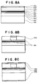
- Figures 8A, 8B, and 8C are sectional views showing how a sixth embodiment of the semiconductor laser device in accordance with the present invention is produced. The layer constitution of the sixth embodiment and how it is produced will be described hereinbelow.
- An insulating film 150 which may be constituted of SiO 2 ,
- stripe portions of the insulating film 150 are removed with an ordinary lithographic technique, such that the middle stripe portion may not be removed.
- the stripe portion remaining at the middle portion of the insulating film 150 is utilized as a mask, and the epitaxial layers ranging from the p-GaAs capping layer 149 to the upper surface of the p-or i-In x1 Ga 1-x1 As 1-y1 P y1 optical waveguide layer 147 are removed with a wet etching technique. In this manner, a ridge stripe is formed.
- etching stops automatically at the upper surface of the p- or i-In x1 Ga 1-x1 As 1-y1 P y1 optical waveguide layer 147.
- an n-In 0.48 (Al z1 Ga 1-z1 ) 0.52 P current blocking layer 151 is formed through selective growth.
- the current blocking layer 151 has a refractive index smaller than that of the cladding layer 148, has a thickness of approximately 1 ⁇ m, and is lattice matched with the substrate 141.
- composition of the n-In 0.48 (Al z1 Ga 1-z1 ) 0.52 P current blocking layer 151 and the thickness of the p- or i-In x1 Ga 1-x1 As 1-y1 P y1 optical waveguide layer 147 are adjusted such that the refractive index guiding in a fundamental transverse mode through the ridge stripe waveguide, which has been formed in the manner described above at the middle portion of the resonator, can be achieved until a laser beam having a high intensity is radiated.
- the insulating film 150 is removed, and a p-GaAs contact layer 152 is formed. Also, a p-side electrode 153 is formed on the p-GaAs contact layer 152. Thereafter, the bottom surface of the substrate 141 is polished, and an n-side electrode 154 is formed on the bottom surface of the substrate 141.
- high-reflectivity coating is carried out on one of resonator surfaces, which have been formed by cleaving the sample, and low-reflectivity coating is carried out on the other resonator surface. Chip formation is then carried out. In this manner, the semiconductor laser device is formed.
- a laser beam having a wavelength of the 0.8 ⁇ m band, which has a high intensity, can be produced while the fundamental transverse mode is being kept.
- the narrow stripe fundamental transverse mode laser is formed.
- the structure described above is also applicable to a wide stripe multi-mode laser.
- the thickness of the optical waveguide layer may be set such that it may fall within the range of 50nm to 400nm.
- each tensile strained barrier layer may have a ternary In x2 Ga 1-x2 P composition.
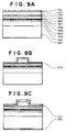
- Figures 9A, 9B, and 9C are sectional views showing how a seventh embodiment of the semiconductor laser device in accordance with the present invention is produced. The layer constitution of the seventh embodiment and how it is produced will be described hereinbelow.
- An insulating film 172 which may be constituted of SiO 2 , or the like, is then formed on the p-GaAs contact layer 171.
- the p-In x4 Ga 1-x4 As 1-y4 P y4 etching blocking layer 169 has a composition, which is lattice matched with the substrate 161 and has a band gap larger than that of the quantum well active layer 165.
- stripe portions of the insulating film 172 are removed with an ordinary lithographic technique, such that the middle stripe portion may not be removed.
- the stripe portion remaining at the middle portion of the insulating film 172 is utilized as a mask, and the epitaxial layers ranging from the p-GaAs contact layer 171 to the upper surface of the p-In x4 Ga 1-x4 As 1-y4 P y4 etching blocking layer 169 are removed with a wet etching technique. In this manner, a ridge stripe is formed.
- the thickness of the p- or i-In x1 Ga 1-x1 As 1-y1 P y1 optical waveguide layer 167 and the thickness of the p-In 0.48 Ga 0.52 P upper first cladding layer 168 are adjusted such that the refractive index guiding in a fundamental transverse mode through the ridge stripe waveguide, which has been formed in the manner described above at the middle portion of the resonator, can be achieved until a laser beam having a high intensity is radiated.
- the insulating film 172 is removed, and an insulating film 173 is formed.
- the portion of the insulating film 173 at the top of the ridge stripe portion is then removed with an ordinary lithographic technique.
- a p-side electrode 174 is formed such that it may cover the exposed contact layer 171.
- the bottom surface of the substrate 161 is polished, and an n-side electrode 175 is formed on the bottom surface of the substrate 161.
- high-reflectivity coating is carried out on one of resonator surfaces, which have been formed by cleaving the sample, and low-reflectivity coating is carried out on the other resonator surface. Chip formation is then carried out. In this manner, the semiconductor laser device is formed.
- a laser beam having a wavelength of the 0.8 ⁇ m band, which has a high intensity, can be produced while the fundamental transverse mode is being kept.
- the narrow stripe fundamental transverse mode laser is formed.
- the structure described above is also applicable to a wide stripe multi-mode laser.
- the total thickness of the optical waveguide layer and the upper first cladding layer may be set such that it may fall within the range of 100nm to 400nm.
- each tensile strained barrier layer may have a ternary In x2 Ga 1-x2 P composition.
- FIG. 10 is a sectional view showing an eighth embodiment of the semiconductor laser device in accordance with the present invention. The layer constitution of the eighth embodiment and how it is produced will be described hereinbelow.
- a p-side electrode 210 is formed on the p-GaAs contact layer 209. Thereafter, the bottom surface of the substrate 201 is polished, and an n-side electrode 211 is formed on the bottom surface of the substrate 201. Thereafter, high-reflectivity coating is carried out on one of resonator surfaces, which have been formed by cleaving the sample, and low-reflectivity coating is carried out on the other resonator surface. Chip formation is then carried out. In this manner, the semiconductor laser device is formed.
- a laser beam having a wavelength of the 0.8 ⁇ m band, which has a high intensity, can be produced while the fundamental transverse mode is being kept.
- the eighth embodiment described above is constituted such that the electrode may be formed over the entire area of the surface of the contact layer 209.
- the semiconductor laser device in accordance with the present invention may be constituted as a gain guiding type of stripe laser, in which an insulating film stripe is formed on the structure described above.
- the semiconductor layer constitution in the eighth embodiment of the semiconductor laser device may be employed for a semiconductor laser provided with a refractive index guiding mechanism, which is produced with ordinary photo-lithographic and dry etching techniques.
- the semiconductor layer constitution may also be employed for a semiconductor laser provided with a diffraction grating, an integrated optical circuit, and the like.
- the GaAs substrate 201 has the n-type electrical conductivity.
- a substrate having the p-type electrical conductivity may be employed. In such cases, all of the electrical conductivity characteristics described above may be reversed.
- the quantum well active layer 205 may also have a multiple quantum well structure. However, the product of the tensile strain quantity of the active layer 205 and the total thickness (the total layer thickness) of the active layer 205 should be at most 0.1nm. Also, each tensile strained barrier layer may have a ternary In x2 Ga 1-x2 P composition.
- Figures 11A, 11B, and 11C are sectional views showing how a ninth embodiment of the semiconductor laser device in accordance with the present invention is produced. The layer constitution of the ninth embodiment and how it is produced will be described hereinbelow.
- stripe portions of the insulating film 230 are removed with an ordinary lithographic technique, such that the middle stripe portion may not be removed.
- the stripe portion remaining at the middle portion of the insulating film 230 is utilized as a mask, and the epitaxial layers ranging from the p-GaAs contact layer 229 to the upper surface of the p-or i-In x1 Ga 1-x1 As 1-y1 P y1 optical waveguide layer 227 are removed with a wet etching technique. In this manner, a ridge stripe is formed.
- etching stops automatically at the upper surface of the p- or i-In x1 Ga 1-x1 As 1-y1 P y1 optical waveguide layer 227.
- the thickness of the p- or i-In x1 Ga 1-x1 As 1-y1 P y1 optical waveguide layer 227 is adjusted such that the refractive index guiding in a fundamental transverse mode through the ridge stripe waveguide, which has been formed in the manner described above at the middle portion of the resonator, can be achieved until a laser beam having a high intensity is radiated.
- the insulating film 230 is removed, and an insulating film 231 is formed over the entire areas of the surfaces of the ridge portion and the exposed optical waveguide layer 227.
- the portion of the insulating film 231 at the top of the ridge stripe portion is then removed with an ordinary lithographic technique.
- a p-side electrode 232 is formed such that it may cover the exposed contact layer 229.
- the bottom surface of the substrate 221 is polished, and an n-side electrode 233 is formed on the bottom surface of the substrate 221.
- high-reflectivity coating is carried out on one of resonator surfaces, which have been formed by cleaving the sample, and low-reflectivity coating is carried out on the other resonator surface. Chip formation is then carried out. In this manner, the semiconductor laser device is formed.
- a laser beam having a wavelength of the 0.8 ⁇ m band, which has a high intensity, can be produced while the fundamental transverse mode is being kept.
- the narrow stripe fundamental transverse mode laser is formed.
- the structure described above is also applicable to a wide stripe multi-mode laser.
- the thickness of the optical waveguide layer may be set such that it may fall within the range of 50nm to 400nm.
- each tensile strained barrier layer may have a quarternary In x2 Ga 1-x2 As 1-y2 P y2 composition.
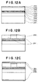
- Figures 12A, 12B, and 12C are sectional views showing how a tenth embodiment of the semiconductor laser device in accordance with the present invention is produced. The layer constitution of the tenth embodiment and how it is produced will be described hereinbelow.
- stripe portions of the insulating film 250 are removed with an ordinary lithographic technique, such that the middle stripe portion may not be removed.
- the stripe portion remaining at the middle portion of the insulating film 250 is utilized as a mask, and the epitaxial layers ranging from the p-GaAs capping layer 249 to the upper surface of the p-or i-In x1 Ga 1-x1 As 1-y1 P y1 optical waveguide layer 247 are removed with a wet etching technique. In this manner, a ridge stripe is formed.
- etching stops automatically at the upper surface of the p- or i-In x1 Ga 1-x1 As 1-y1 P y1 optical waveguide layer 247.
- an n-In 0.48 (Al z1 Ga 1-z1 ) 0.52 P current blocking layer 251 is formed through selective growth.
- the current blocking layer 251 has a refractive index smaller than that of the cladding layer 248, has a thickness of approximately 1 ⁇ m, and is lattice matched with the substrate 241.
- composition of the n-In 0.48 (Al z1 Ga 1-z1 ) 0.52 P current blocking layer 251 and the thickness of the p- or i-In x1 Ga 1-x1 As 1-y1 P y1 optical waveguide layer 247 are adjusted such that the refractive index guiding in a fundamental transverse mode through the ridge stripe waveguide, which has been formed in the manner described above at the middle portion of the resonator, can be achieved until a laser beam having a high intensity is radiated.
- the insulating film 250 is removed, and a p-GaAs contact layer 252 is formed. Also, a p-side electrode 253 is formed on the p-GaAs contact layer 252. Thereafter, the bottom surface of the substrate 241 is polished, and an n-side electrode 254 is formed on the bottom surface of the substrate 241.
- high-reflectivity coating is carried out on one of resonator surfaces, which have been formed by cleaving the sample, and low-reflectivity coating is carried out on the other resonator surface. Chip formation is then carried out. In this manner, the semiconductor laser device is formed.
- a laser beam having a wavelength of the 0.8 ⁇ m band, which has a high intensity, can be produced while the fundamental transverse mode is being kept.
- the narrow stripe fundamental transverse mode laser is formed.
- the structure described above is also applicable to a wide stripe multi-mode laser.
- the thickness of the optical waveguide layer may be set such that it may fall within the range of 50nm to 400nm.
- each tensile strained barrier layer may have a ternary In x2 Ga 1-x2 P composition.
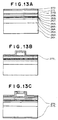
- FIGS 13A, 13B, and 13C are sectional views showing how an eleventh embodiment of the semiconductor laser device in accordance with the present invention is produced. The layer constitution of the eleventh embodiment and how it is produced will be described hereinbelow.
- the p-In x4 Ga 1-x4 As 1-y4 P y4 etching blocking layer 269 has a composition, which is lattice matched with the substrate 261 and has a band gap larger than that of the quantum well active layer 265.
- stripe portions of the insulating film 272 are removed with an ordinary lithographic technique, such that the middle stripe portion may not be removed.
- the stripe portion remaining at the middle portion of the insulating film 272 is utilized as a mask, and the epitaxial layers ranging from the p-GaAs contact layer 271 to the upper surface of the p-In x4 Ga 1-x4 As 1-y4 P y4 etching blocking layer 269 are removed with a wet etching technique. In this manner, a ridge stripe is formed.
- etching stops automatically at the upper surface of the p-In x4 Ga 1-x4 As 1-y4 P y4 etching blocking layer 269.
- the thickness of the p- or i-In x1 Ga 1-x1 As 1-y1 P y1 optical waveguide layer 267 and the thickness of the p-In 0.48 (Al z Ga 1-z ) 0.52 P upper first cladding layer 268 are adjusted such that the refractive index guiding in a fundamental transverse mode through the ridge stripe waveguide, which has been formed in the manner described above at the middle portion of the resonator, can be achieved until a laser beam having a high intensity is radiated.
- the insulating film 272 is removed, and an insulating film 273 is formed.
- the portion of the insulating film 273 at the top of the ridge stripe portion is then removed with an ordinary lithographic technique.
- a p-side electrode 274 is formed such that it may cover the exposed contact layer 271.
- the bottom surface of the substrate 261 is polished, and an n-side electrode 275 is formed on the bottom surface of the substrate 261.
- high-reflectivity coating is carried out on one of resonator surfaces, which have been formed by cleaving the sample, and low-reflectivity coating is carried out on the other resonator surface. Chip formation is then carried out. In this manner, the semiconductor laser device is formed.
- a laser beam having a wavelength of the 0.8 ⁇ m band, which has a high intensity, can be produced while the fundamental transverse mode is being kept.
- the narrow stripe fundamental transverse mode laser is formed.
- the structure described above is also applicable to a wide stripe multi-mode laser.
- the total thickness of the optical waveguide layer and the upper first cladding layer may be set such that it may fall within the range of 100nm to 400nm.
- each tensile strained barrier layer may have a ternary In x2 Ga 1-x2 P composition.
- the GaAs substrate 261 has the n-type electrical conductivity.
- a substrate having the p-type electrical conductivity may be employed. In such cases, all of the electrical conductivity characteristics described above may be reversed.
- the embodiments described above have the structures referred to as SQW-SCH, wherein a single quantum well is provided and the compositions of the optical waveguide layers are identical with each other.
- the semiconductor laser device in accordance with the present invention is also applicable to an MQW structure, wherein a plurality of quantum wells are provided.
- composition ratio of the In x3 Ga 1-x3 As 1-y3 P y3 quantum well active layer, or the like may be adjusted such that a laser beam having a wavelength falling within the range of 750nm ⁇ 850nm may be radiated.
- the semiconductor layer growth method besides the metalorganic chemical vapor deposition process described above, it is also possible to employ the molecular-beam epitaxial growth method utilizing a solid or a gas as the raw material.
- the semiconductor laser device in accordance with the present invention can also be utilized as a light source for use in the fields of quick information processing, quick image processing, communication, measurement, medical applications, printing, and the like.
Landscapes
- Physics & Mathematics (AREA)
- Optics & Photonics (AREA)
- Condensed Matter Physics & Semiconductors (AREA)
- General Physics & Mathematics (AREA)
- Electromagnetism (AREA)
- Chemical & Material Sciences (AREA)
- Engineering & Computer Science (AREA)
- Nanotechnology (AREA)
- Life Sciences & Earth Sciences (AREA)
- Biophysics (AREA)
- Crystallography & Structural Chemistry (AREA)
- Semiconductor Lasers (AREA)
Applications Claiming Priority (6)
| Application Number | Priority Date | Filing Date | Title |
|---|---|---|---|
| JP32317697 | 1997-11-25 | ||
| JP323176/97 | 1997-11-25 | ||
| JP32317697 | 1997-11-25 | ||
| JP31764498 | 1998-11-09 | ||
| JP31764498A JP3753216B2 (ja) | 1997-11-25 | 1998-11-09 | 半導体レーザ装置 |
| JP317644/98 | 1998-11-09 |
Publications (3)
| Publication Number | Publication Date |
|---|---|
| EP0920096A2 true EP0920096A2 (fr) | 1999-06-02 |
| EP0920096A3 EP0920096A3 (fr) | 1999-07-14 |
| EP0920096B1 EP0920096B1 (fr) | 2001-10-10 |
Family
ID=26569090
Family Applications (1)
| Application Number | Title | Priority Date | Filing Date |
|---|---|---|---|
| EP98122308A Expired - Lifetime EP0920096B1 (fr) | 1997-11-25 | 1998-11-24 | Laser à semi-conducteur |
Country Status (4)
| Country | Link |
|---|---|
| US (1) | US6127691A (fr) |
| EP (1) | EP0920096B1 (fr) |
| JP (1) | JP3753216B2 (fr) |
| DE (1) | DE69801974T2 (fr) |
Cited By (2)
| Publication number | Priority date | Publication date | Assignee | Title |
|---|---|---|---|---|
| EP1198042A3 (fr) * | 2000-10-12 | 2004-04-28 | Fuji Photo Film Co., Ltd. | Laser à semi-conducteur avec région sans injection de courant à proximité d'une face de resonateur et son procédé de fabrication |
| US7197056B2 (en) | 2001-11-15 | 2007-03-27 | Sharp Kabushiki Kaisha | Semiconductor laser device and optical disc drive |
Families Citing this family (25)
| Publication number | Priority date | Publication date | Assignee | Title |
|---|---|---|---|---|
| JPH11233815A (ja) * | 1998-02-13 | 1999-08-27 | Furukawa Electric Co Ltd:The | 半導体発光ダイオード |
| JP3434706B2 (ja) * | 1998-05-21 | 2003-08-11 | 富士写真フイルム株式会社 | 半導体レーザおよびその製造方法 |
| US6219365B1 (en) * | 1998-11-03 | 2001-04-17 | Wisconsin Alumni Research Foundation | High performance aluminum free active region semiconductor lasers |
| US6542528B1 (en) | 1999-02-15 | 2003-04-01 | Ricoh Company, Ltd. | Light-emitting semiconductor device producing red wavelength optical radiation |
| JP2001308466A (ja) * | 2000-04-24 | 2001-11-02 | Fuji Photo Film Co Ltd | 半導体レーザ装置 |
| JP2002026453A (ja) * | 2000-07-03 | 2002-01-25 | Mitsubishi Electric Corp | リッジ導波路型半導体レーザ及びその製造方法 |
| JP2002204032A (ja) * | 2000-10-31 | 2002-07-19 | Fuji Photo Film Co Ltd | 半導体レーザ素子 |
| JP2002305352A (ja) * | 2001-04-05 | 2002-10-18 | Fuji Photo Film Co Ltd | 半導体レーザ素子 |
| JP2003283056A (ja) | 2002-01-15 | 2003-10-03 | Sharp Corp | 半導体レーザ装置および光ディスク再生記録装置 |
| JP2003289175A (ja) | 2002-01-28 | 2003-10-10 | Sharp Corp | 半導体レーザ素子 |
| JP4927807B2 (ja) * | 2002-01-28 | 2012-05-09 | シャープ株式会社 | 半導体レーザ素子 |
| US7801194B2 (en) | 2002-07-01 | 2010-09-21 | Sharp Kabushiki Kaisha | Semiconductor laser device and optical disk unit using the same |
| US7378681B2 (en) * | 2002-08-12 | 2008-05-27 | Agility Communications, Inc. | Ridge waveguide device surface passivation by epitaxial regrowth |
| JP2004158615A (ja) * | 2002-11-06 | 2004-06-03 | Mitsubishi Electric Corp | 半導体レーザ装置 |
| JP2004296634A (ja) * | 2003-03-26 | 2004-10-21 | Sharp Corp | 半導体レーザ装置および光ディスク装置 |
| JP2004296637A (ja) | 2003-03-26 | 2004-10-21 | Sharp Corp | 半導体レーザ装置および光ディスク装置 |
| JP4262549B2 (ja) * | 2003-07-22 | 2009-05-13 | シャープ株式会社 | 半導体レーザ素子およびその製造方法 |
| US7687291B2 (en) | 2005-03-25 | 2010-03-30 | Trumpf Photonics Inc. | Laser facet passivation |
| US7403552B2 (en) * | 2006-03-10 | 2008-07-22 | Wisconsin Alumni Research Foundation | High efficiency intersubband semiconductor lasers |
| US7457338B2 (en) * | 2006-04-19 | 2008-11-25 | Wisconsin Alumni Research Foundation | Quantum well lasers with strained quantum wells and dilute nitride barriers |
| TWI341600B (en) * | 2007-08-31 | 2011-05-01 | Huga Optotech Inc | Light optoelectronic device and forming method thereof |
| DE102007057708A1 (de) * | 2007-09-26 | 2009-04-09 | Osram Opto Semiconductors Gmbh | Optoelektronisches Bauelement |
| US9716368B2 (en) * | 2015-07-02 | 2017-07-25 | Sae Magnetics (H.K.) Ltd. | Tunable optical phase filter |
| US10043941B1 (en) | 2017-01-31 | 2018-08-07 | International Business Machines Corporation | Light emitting diode having improved quantum efficiency at low injection current |
| CN110854678B (zh) * | 2018-08-20 | 2021-02-05 | 山东华光光电子股份有限公司 | 一种GaAs基大功率激光器制备方法 |
Family Cites Families (5)
| Publication number | Priority date | Publication date | Assignee | Title |
|---|---|---|---|---|
| US5488233A (en) * | 1993-03-11 | 1996-01-30 | Kabushiki Kaisha Toshiba | Semiconductor light-emitting device with compound semiconductor layer |
| US5389396A (en) * | 1993-08-11 | 1995-02-14 | Northwestern University | InGaAsP/GaAs diode laser |
| US5617437A (en) * | 1994-11-24 | 1997-04-01 | Fuji Photo Film Co., Ltd. | Semiconductor laser |
| US5663976A (en) * | 1995-10-16 | 1997-09-02 | Northwestern University | Buried-ridge laser device |
| JPH09270558A (ja) * | 1996-03-29 | 1997-10-14 | Fuji Photo Film Co Ltd | 半導体レーザ |
-
1998
- 1998-11-09 JP JP31764498A patent/JP3753216B2/ja not_active Expired - Fee Related
- 1998-11-24 EP EP98122308A patent/EP0920096B1/fr not_active Expired - Lifetime
- 1998-11-24 DE DE69801974T patent/DE69801974T2/de not_active Expired - Lifetime
- 1998-11-25 US US09/199,815 patent/US6127691A/en not_active Expired - Lifetime
Cited By (5)
| Publication number | Priority date | Publication date | Assignee | Title |
|---|---|---|---|---|
| EP1198042A3 (fr) * | 2000-10-12 | 2004-04-28 | Fuji Photo Film Co., Ltd. | Laser à semi-conducteur avec région sans injection de courant à proximité d'une face de resonateur et son procédé de fabrication |
| US6888866B2 (en) | 2000-10-12 | 2005-05-03 | Fuji Photo Film Co., Ltd. | Semiconductor laser device with a current non-injection region near a resonator end face, and fabrication method thereof |
| EP1583187A1 (fr) * | 2000-10-12 | 2005-10-05 | Fuji Photo Film Co., Ltd | Laser à semi-conducteur avec région sans injection de courant à proximité d'une face de résonateur |
| US7197056B2 (en) | 2001-11-15 | 2007-03-27 | Sharp Kabushiki Kaisha | Semiconductor laser device and optical disc drive |
| EP1455427B1 (fr) * | 2001-11-15 | 2008-07-23 | Sharp Kabushiki Kaisha | Dispositif laser a semi-conducteurs et dispositif d'entrainement de disque optique |
Also Published As
| Publication number | Publication date |
|---|---|
| EP0920096B1 (fr) | 2001-10-10 |
| DE69801974D1 (de) | 2001-11-15 |
| EP0920096A3 (fr) | 1999-07-14 |
| JP3753216B2 (ja) | 2006-03-08 |
| JPH11220224A (ja) | 1999-08-10 |
| DE69801974T2 (de) | 2002-04-04 |
| US6127691A (en) | 2000-10-03 |
Similar Documents
| Publication | Publication Date | Title |
|---|---|---|
| EP0920096B1 (fr) | Laser à semi-conducteur | |
| EP0814548B1 (fr) | Laser à semi-conducteur | |
| EP1104057B1 (fr) | Laser à semiconducteur à haute puissance avec confinement de courant et à guidage par indice | |
| EP0936709B1 (fr) | Laser à semi-conducteur | |
| US6580738B2 (en) | High-power semiconductor laser device in which near-edge portions of active layer are removed | |
| JP3859839B2 (ja) | 屈折率導波型半導体レーザ装置 | |
| US5617437A (en) | Semiconductor laser | |
| US6400743B1 (en) | High-power semiconductor laser device having current confinement structure and index-guided structure | |
| US20020044584A1 (en) | Semiconductor laser device which includes AlGaAs optical waveguide layer being formed over internal stripe groove and having controlled refractive index | |
| US6973109B2 (en) | Semiconductor laser device having strain buffer layer between compressive-strain quantum well layer and tensile-strain barrier layer | |
| KR100771082B1 (ko) | 반도체 레이저소자 및 그 제조방법 | |
| JP4033930B2 (ja) | 半導体レーザ | |
| JP2000114654A (ja) | 半導体レーザ装置 | |
| US20030133484A1 (en) | Semiconductor laser and method of producing the same | |
| JP2001284704A (ja) | 半導体レーザ装置 | |
| JP2001308466A (ja) | 半導体レーザ装置 | |
| EP1251609B1 (fr) | Dispositif laser à haute puissance à structure à fenêtre | |
| JPH1197794A (ja) | 半導体レーザ装置 | |
| JP3654315B2 (ja) | 半導体レーザ | |
| JP2001298241A (ja) | 半導体レーザ装置 | |
| US6873637B2 (en) | Semiconductor laser element including optical waveguide layers which have gradually varying bandgaps so as to reduce electrical resistance at interfaces | |
| JP2003023218A (ja) | 半導体レーザ素子 | |
| JPH11284275A (ja) | 半導体レーザ | |
| JP2003347679A (ja) | 半導体レーザ素子 | |
| JP3667883B2 (ja) | 半導体レーザ素子 |
Legal Events
| Date | Code | Title | Description |
|---|---|---|---|
| PUAI | Public reference made under article 153(3) epc to a published international application that has entered the european phase |
Free format text: ORIGINAL CODE: 0009012 |
|
| PUAL | Search report despatched |
Free format text: ORIGINAL CODE: 0009013 |
|
| AK | Designated contracting states |
Kind code of ref document: A2 Designated state(s): DE FR GB |
|
| AX | Request for extension of the european patent |
Free format text: AL;LT;LV;MK;RO;SI |
|
| AK | Designated contracting states |
Kind code of ref document: A3 Designated state(s): AT BE CH CY DE DK ES FI FR GB GR IE IT LI LU MC NL PT SE |
|
| AX | Request for extension of the european patent |
Free format text: AL;LT;LV;MK;RO;SI |
|
| 17P | Request for examination filed |
Effective date: 19990831 |
|
| AKX | Designation fees paid |
Free format text: DE FR GB |
|
| RIC1 | Information provided on ipc code assigned before grant |
Free format text: 7H 01S 5/343 A |
|
| GRAG | Despatch of communication of intention to grant |
Free format text: ORIGINAL CODE: EPIDOS AGRA |
|
| RIC1 | Information provided on ipc code assigned before grant |
Free format text: 7H 01S 3/19 A |
|
| 17Q | First examination report despatched |
Effective date: 20001218 |
|
| GRAG | Despatch of communication of intention to grant |
Free format text: ORIGINAL CODE: EPIDOS AGRA |
|
| GRAH | Despatch of communication of intention to grant a patent |
Free format text: ORIGINAL CODE: EPIDOS IGRA |
|
| GRAH | Despatch of communication of intention to grant a patent |
Free format text: ORIGINAL CODE: EPIDOS IGRA |
|
| GRAA | (expected) grant |
Free format text: ORIGINAL CODE: 0009210 |
|
| RIC1 | Information provided on ipc code assigned before grant |
Free format text: 7H 01S 5/343 A |
|
| AK | Designated contracting states |
Kind code of ref document: B1 Designated state(s): DE FR GB |
|
| REF | Corresponds to: |
Ref document number: 69801974 Country of ref document: DE Date of ref document: 20011115 |
|
| REG | Reference to a national code |
Ref country code: GB Ref legal event code: IF02 |
|
| ET | Fr: translation filed | ||
| PLBE | No opposition filed within time limit |
Free format text: ORIGINAL CODE: 0009261 |
|
| STAA | Information on the status of an ep patent application or granted ep patent |
Free format text: STATUS: NO OPPOSITION FILED WITHIN TIME LIMIT |
|
| 26N | No opposition filed | ||
| REG | Reference to a national code |
Ref country code: GB Ref legal event code: 732E |
|
| REG | Reference to a national code |
Ref country code: FR Ref legal event code: TP Ref country code: FR Ref legal event code: CD |
|
| REG | Reference to a national code |
Ref country code: DE Ref legal event code: R082 Ref document number: 69801974 Country of ref document: DE Representative=s name: KLUNKER, SCHMITT-NILSON, HIRSCH, DE |
|
| REG | Reference to a national code |
Ref country code: DE Ref legal event code: R082 Ref document number: 69801974 Country of ref document: DE Representative=s name: KLUNKER, SCHMITT-NILSON, HIRSCH, DE Effective date: 20120521 Ref country code: DE Ref legal event code: R081 Ref document number: 69801974 Country of ref document: DE Owner name: NICHIA CORP., ANAN-SHI, JP Free format text: FORMER OWNER: FUJIFILM CORP., TOKIO/TOKYO, JP Effective date: 20120521 |
|
| REG | Reference to a national code |
Ref country code: GB Ref legal event code: 732E Free format text: REGISTERED BETWEEN 20120621 AND 20120627 |
|
| REG | Reference to a national code |
Ref country code: FR Ref legal event code: TP Owner name: NICHIA CORPORATION, JP Effective date: 20120806 |
|
| PGFP | Annual fee paid to national office [announced via postgrant information from national office to epo] |
Ref country code: GB Payment date: 20141119 Year of fee payment: 17 Ref country code: DE Payment date: 20141118 Year of fee payment: 17 Ref country code: FR Payment date: 20141110 Year of fee payment: 17 |
|
| REG | Reference to a national code |
Ref country code: DE Ref legal event code: R119 Ref document number: 69801974 Country of ref document: DE |
|
| GBPC | Gb: european patent ceased through non-payment of renewal fee |
Effective date: 20151124 |
|
| REG | Reference to a national code |
Ref country code: FR Ref legal event code: ST Effective date: 20160729 |
|
| PG25 | Lapsed in a contracting state [announced via postgrant information from national office to epo] |
Ref country code: GB Free format text: LAPSE BECAUSE OF NON-PAYMENT OF DUE FEES Effective date: 20151124 Ref country code: DE Free format text: LAPSE BECAUSE OF NON-PAYMENT OF DUE FEES Effective date: 20160601 |
|
| PG25 | Lapsed in a contracting state [announced via postgrant information from national office to epo] |
Ref country code: FR Free format text: LAPSE BECAUSE OF NON-PAYMENT OF DUE FEES Effective date: 20151130 |