EP0921404A2 - Procédé de mesure pour des caractéristiques en hautes fréquences des matériaux diélectriques et procédé de conception des circuits haute fréquence - Google Patents
Procédé de mesure pour des caractéristiques en hautes fréquences des matériaux diélectriques et procédé de conception des circuits haute fréquence Download PDFInfo
- Publication number
- EP0921404A2 EP0921404A2 EP98121710A EP98121710A EP0921404A2 EP 0921404 A2 EP0921404 A2 EP 0921404A2 EP 98121710 A EP98121710 A EP 98121710A EP 98121710 A EP98121710 A EP 98121710A EP 0921404 A2 EP0921404 A2 EP 0921404A2
- Authority
- EP
- European Patent Office
- Prior art keywords
- high frequency
- transmission line
- electric field
- wavelength
- circuit design
- Prior art date
- Legal status (The legal status is an assumption and is not a legal conclusion. Google has not performed a legal analysis and makes no representation as to the accuracy of the status listed.)
- Withdrawn
Links
Images





Classifications
-
- G—PHYSICS
- G01—MEASURING; TESTING
- G01R—MEASURING ELECTRIC VARIABLES; MEASURING MAGNETIC VARIABLES
- G01R27/00—Arrangements for measuring resistance, reactance, impedance, or electric characteristics derived therefrom
- G01R27/02—Measuring real or complex resistance, reactance, impedance, or other two-pole characteristics derived therefrom, e.g. time constant
- G01R27/26—Measuring inductance or capacitance; Measuring quality factor, e.g. by using the resonance method; Measuring loss factor; Measuring dielectric constants ; Measuring impedance or related variables
- G01R27/2617—Measuring dielectric properties, e.g. constants
- G01R27/2635—Sample holders, electrodes or excitation arrangements, e.g. sensors or measuring cells
-
- G—PHYSICS
- G01—MEASURING; TESTING
- G01R—MEASURING ELECTRIC VARIABLES; MEASURING MAGNETIC VARIABLES
- G01R15/00—Details of measuring arrangements of the types provided for in groups G01R17/00 - G01R29/00, G01R33/00 - G01R33/26 or G01R35/00
- G01R15/14—Adaptations providing voltage or current isolation, e.g. for high-voltage or high-current networks
- G01R15/24—Adaptations providing voltage or current isolation, e.g. for high-voltage or high-current networks using light-modulating devices
- G01R15/241—Adaptations providing voltage or current isolation, e.g. for high-voltage or high-current networks using light-modulating devices using electro-optical modulators, e.g. electro-absorption
- G01R15/242—Adaptations providing voltage or current isolation, e.g. for high-voltage or high-current networks using light-modulating devices using electro-optical modulators, e.g. electro-absorption based on the Pockels effect, i.e. linear electro-optic effect
Definitions
- This invention describes an effective measurement method of the high frequency characteristics of dielectric materials which are used for high frequency filters, isolators or couplers having microstrip line structures, or for high frequency capacitors.
- This invention also especially describes an efficient measurement method of the effective dielectric constant and the dielectric loss of dielectric materials, and a high frequency circuit board design method which uses the said measurement method.
- the propagation velocity and the attenuation of the electromagnetic wave propagating in a dielectric material can be derived as follow, respectively, by using the effective dielectric constant and the loss tangent.
- Propagation Velocity: V C / ⁇ ⁇ r
- Attenuation: a f ⁇ ⁇ ⁇ r ⁇ tan ⁇
- C light velocity
- ⁇ r effective dielectric constant
- f frequency
- tan ⁇ loss tangent.
- a measurement method of high frequency characteristics of the dielectric material above all a measurement method of the effective dielectric constant and the dielectric loss is important, especially when the dielectric material is the component of a microstrip line.
- An impedance conversion formulae for a microstrip line (which is a distributed constant line) can be expressed as the following, just as Fig. 14 shows.
- the impedance conversion formula for a microstrip line is determined by the effective dielectric constant( ⁇ reff ) and the line length.
- the effective dielectric constant (the wavelength-shortening ratio), which is given by the following equation (approximation), is usually used.
- ⁇ reff 0.5 ⁇ e 0.5 + ( ⁇ r 0.5 - ⁇ r 0.5 )/(1 + 4F -1.5 )
- F 4h( ⁇ r -1) 0.5 [0.5+ ⁇ 1 + 2log (1 + W/h) ⁇ 2 ]/ ⁇ 0
- ⁇ e ( ⁇ r + 1)/2 + ( ⁇ r - 1)/ ⁇ 2(1 + 10h/W) 0.5 ) ⁇
- ⁇ reff effective dielectric constant at the transmission line
- h thickness of the substrate W : width of the transmission line
- ⁇ 0 signal wavelength in the vacuum
- ⁇ e effective permittivity of the dielectric material
- ⁇ r dielectric constant of the dielectric material.
- Figure 4 is a bird's-eye view of the structure depicted in Figure 3, showing the structure of a tri-plate microstrip line resonator.
- 2 denotes transmission lines having an input port and an output port at each one end
- 3 shows a microstrip line which composes a resonator.
- L is the length of the resonator
- ⁇ L is the electrical correction length
- W denotes the width of the microstrip line.
- the dielectric constant of the dielectric body can be derived from the resonance frequency that is determined by the resonator 3 and the electrical correction length 4.
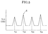
- values of the dielectric constant can be obtained only at resonance frequencies (f01 ⁇ fo4) as shown in Fig. 5, which means that it is impossible to obtain continuous values of the dielectric constant with frequency change, if the resonance method is deployed. Also it is impossible to make adjustment by changing the electrical correction length, because the resonator must have a symmetrical structure in this measurement method.
- dielectric constant ⁇ r and conductor skin resistance R s are unknown. While dielectric constant ⁇ r can be obtained only as discrete values as described above, conductor skin resistance is actually difficult to obtain because it depends on the oxidization status of the conductor surface, on the shape of the conductor cross section, and also on the frequency.
- the purpose of this invention is to provide with a method for continuous and accurate measurement of the effective dielectric constant and the dielectric loss of a dielectric material at the same condition as it is implemented in actual circuits.
- the invention provides with a solution for already explained problems of the conventional resonance method in measuring high frequency characteristics of a dielectric material.
- Another purpose of this invention is to improve the poor accuracy of the conventional high frequency circuit simulators, in order to realize high accuracy in high frequency circuit design.
- This purpose is realized by providing with a design method using the actual wavelength-shortening ratio of the circuit that is obtained through the measurement of circuit impedance at the same condition as the circuit is practically used.
- the high frequency measurement method for dielectric materials of this invention is characterized as; it measures amplitude and phase variations of the electric field component of an electromagnetic wave along its propagation direction on a high frequency transmission line which is actually implemented as a microstrip line, by using a device whose refraction index changes according to the electric field (or an E-O prober using Pockels Effect), in order to get effective dielectric constant and dielectric loss of said transmission line.
- the high frequency circuit design method of this invention is characterized as; phase variation rate of the electric field component of an electromagnetic wave along its propagation direction on a high frequency transmission line which is actually implemented as a microstrip line is measured by using a device whose refraction index changes according to the electric field (or an E-O prober using Pockels Effect), said phase variation rate is used to derive the wavelength-shortening ratio of said transmission line and said wavelength-shortening ratio is used in the high frequency circuit design.
- the high frequency circuit design method of this invention is characterized as; in high frequency circuit design, phase variation rate of the electric field component of an electromagnetic wave along its propagation direction on a high frequency transmission line which is actually implemented as a microstrip line is measured by using a device whose refraction index changes according to the electric field (or an E-O prober using Pockels Effect), said phase variation rate is used to derive the wavelength-shortening ratio of said transmission line, a data table for the high frequency circuit design is generated using said wavelength-shortening ratio and said data table is used in the design.
- z denotes the position along the transmission line
- k ⁇ - j ⁇ .
- the equation (1) shows that exp ⁇ j( ⁇ t - ⁇ z) ⁇ is the phase component and exp(- ⁇ z) is the loss component.
- the following equation can be derived for the loss component.
- wavelength ⁇ of an electromagnetic wave propagating in a dielectric material becomes shorter than wavelength ⁇ 0 in the vacuum.
- ⁇ ⁇ 0 / ⁇ r 1/2
- ⁇ r ⁇ / ⁇ 0 ( ⁇ r >1)
- ⁇ r 1/2 is generally called as wavelength-shortening ratio.
- equations (6) to (8) are derived as the following.
- Figure 1 is a birds-eye view of a microstrip line which is used for the high frequency measurement employing the measurement method of this invention.
- the line 5 in the center of the substrate surface works as a transmission line.
- Points 1 which are shown by symbols ⁇ in the figure denote the measuring points. These measuring points are placed along the propagation direction of the electromagnetic wave, at 5mm intervals from the edge of the transmission line 5.
- Amplitude and phase variations of the electric field component of the electromagnetic wave along its propagation direction on the high frequency transmission line are measured at said measuring points 1, by touching a measuring element whose refraction index changes according to the electric field applied to it.
- the wavelength-shortening ratio can be derived from equation (10), when the phase component in the electric field component of the electromagnetic wave propagating along the transmission is detected at position z.
- the precise value of ⁇ can be obtained since ⁇ is the gradient of phase ⁇ in the direction of z and it does not include errors inherent to measurement instruments.
- the design method of this invention for high frequency circuits that uses an E-O prober is characterizes as; (a) it uses a measuring element whose refraction coefficient changes according to the electromagnetic field applied to it in order to measure the phase component variation ratio against the propagation direction of the electromagnetic wave which propagates along the transmission line, (b) it calculates the transmission wavelength of the transmission line from said phase component variation rate, (c) it derives the wavelength-shortening ratio of said transmission line from the ratio between said transmission wavelength and the wavelength in the vacuum, and (d) it composes an impedance conversion circuit by using the derived wavelength-shortening ratio.
- the precise value of the wavelength-shortening ratio can be obtained by using the measurement method of this invention, since measurement errors usually inherent to measuring instruments can be avoided because the phase value of the electric field component of the electromagnetic wave which propagates along the high frequency transmission line is directly measured, and because the variation rate of said measured phase value against the propagation direction is used for the design.
- This sensor is an ultra-high speed voltage waveform measuring equipment, or so-called E-O prober, which uses a non-contact electric field sensor. Examples of such a sensor are explained in detail in such references as "Highly Sensitive Real Time Electro-Optic Probing for Long Logic Pattern Analysis", Hironori Takahashi, Shin-ichiro Aoshima, Kazuhiko Wakamori, Isuke Hirano and Yutaka Tsuchiya, IEICE Trans. Electron, Vol. E78-C, No.
- the E-O prober is an ultra-high speed voltage waveform measuring equipment for the evaluation of a microwave circuit, consisting of a non-contact electric field sensor and a semiconductor pulse laser.
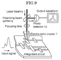
- the E-O prober can measure voltage waveforms inside a device such as an MMIC with high time-resolution and without touching the device nor disturbing the device status. This feature of the E-O prober, which has not been realized by conventional electric measuring methods, comes from its measurement principle shown in Fig. 9.
- an electric field sensor 7 that is composed of an electro-optic crystal is placed near the electrode under measurement.
- the refraction index of the electric field sensor changes according to the applied voltage at said electrode.
- a laser beam 9 is applied to the electric field sensor, the polarization status of the laser beam is changed according to the change in the refraction index of the crystal.
- This optical output is detected by an optical detector 10, and then amplified by a lock-in amplifier or the like, to get an enough level of a voltage waveform.
- the response time of the electro-optic crystal used in the electric field sensor is as fast as less than 1 psec., high time resolution as narrow as the laser pulse width can be obtained, if sampling measurement method using a pulsed laser beam is employed. In addition to this, transmission distortion caused by a transmission line does not exist in this measurement method, since the optical beam is used for measurement.
- the electrical field sensor crystal is attached to a silica-glass holder which is fixed at the top of a metallic or ceramic needle.
- One side length of the sensor is about 200 ⁇ m.
- the electric field sensor detects the leaked electric field from the electrode, so that the sensor need not touch the electrode. Since the laser beam is reflected by the mirror surface of the electric field sensor bottom, it does not reach to the electrode. Thus the laser beam does not affect the behavior of the measured device.
- the electric field sensor works as a load for the electrode to be measured, its capacitance is very small. As a result it affects the electrode little, enabling the non-intrusive measurement.
- the measurable area of the electric field sensor is determined by the focused optical beam diameter, which allows measuring anywhere in an IC, as far as the sensor can access.
- a device whose refraction index changes according to the electric field is not limited to the device using Pockels effect (refraction index changes in proportion to the electric field).
- a device using Kerr effect (refraction index changes in proportion to the square of the electric field) may be also used.
- FIG 10 shows the structure of E-O prober equipment.
- the main body of the E-O prober is assembled on a probe station 11 for microwave devices, and is used as a microscope for observation.
- An E-O head 12, which is the electric field sensor, is set under an object lens 13, and is moved by a motor driven from an external controller.
- a semiconductor laser LD is contained in a control unit 14, and the laser light enters into or comes out from the main body through an optical fiber 15.
- An output from the main oscillator 16 of a signal source which is 10MHz for example, is fed to the control unit 16 and is used as a triggering signal, in order to synchronize the optical output to the device under measurement.
- the semiconductor laser lights synchronous to this triggering signal, at the frequency of 1 MHz, for example.
- the measuring operation is carried out on a personal computer 17. Watching a microscopic image on the personal computer monitor, measurement position is determined first by manipulating an XY stage 18 from outside. Then, after bringing the E-O head near to the electrode to be measured by using an auto-focusing function, measurement begins. Processed waveform data are displayed on the personal computer. Amplitude and phase information in the frequency domain can be derived by using Fast Fourier Transform (FFT). By using such a simple method as described above, a voltage waveform at any arbitrary point in an IC can be obtained, just as like as the measurement using a sampling oscilloscope.
- FFT Fast Fourier Transform
- the timing of the measurement at the measuring point is kept constant even if the electric field sensor is moved on the device under measurement.
- the device under measurement is a microstrip line, and that an impulse wave is applied to the transmission line.
- the waveform measured at the output end is time delayed as compared to the waveform measured at the input end. This delay, which is previously mentioned ⁇ , depends on the propagation velocity of the voltage wave propagating on the transmission line. If the waveform attenuates because the electric resistance of the transmission line is large, the amplitude of the waveform at the output port becomes small, so that previously mentioned ⁇ is measured.
- the impedance of the electric field sensor in the E-O prober is so large that the sensor does not affect the behavior of the device under test.
- the transmission line is fabricated on a substrate made from a dielectric material with a certain value of permittivity
- the propagation velocity of the waveform on the transmission line depends mainly on the dielectric constant of the substrate.
- the attenuation of the waveform depends on the loss tangent of the substrate.
- the double refraction coefficient of the E-O crystal is changed according to the electric field intensity, when the electric field on the transmission line is coupled to the E-O crystal as described above. If the pulsed laser light is injected to the E-O crystal at this condition, the polarization status of the laser light is changed, and thus the waveform of the signal under measurement can be observed.
- the spatial resolution, the frequency bandwidth and the measurement sensitivity of the E-O prober used here are 5 ⁇ m, 20GHz and 50mV, respectively.
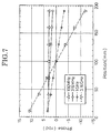
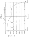
- Figures 7, and 8 show measurement examples for a dielectric material.
- the value of ⁇ can be derived by using Equation (2) from the measured loss characteristic curve (Fig. 8) of the electric field at each measuring point. Also, The value of ⁇ can be derived from the electric field variation at each measuring point (the slope of each line in Fig. 7). Consequently, the effective dielectric constant and the dielectric loss can be calculated by applying values of ⁇ and ⁇ derived as above to equations (6), (7) and (8).
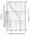
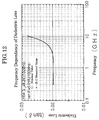
- Tables 1 and 2 show the experiment result and the calculation result. These results are illustrated as figures in Fig. 11 and Fig. 12, respectively.
- the wavelength-shortening ratio in Fig. 11 is the very important factor for circuit design, and the dielectric loss curve in Fig. 12 is also very important data for evaluating high frequency characteristics of a dielectric material.
- Fig. 11 shows similar data plots as the conventional empirical analysis curve, the analyzed values are merely supposed values based on empiricism. Additionally this analysis is complex and needs much calculation time. Considering all of these factors, and taking into consideration that the method is much simpler and the measurement results are much more accurate and reliable, it is evident that the measuring method of this invention is much superior to conventional methods.
- Fig. 12 shows the nominal dielectric loss of the dielectric material used in the measurement. As previously mentioned, it is not the value at a high frequency, especially at 1GHz or higher, but the one at a low frequency. This is only because there are no conventional ways to measure dielectric loss in the high frequency region, so that the value at the lower frequency is substituted. However, as Fig. 12 shows, the dielectric loss characteristics in the high frequency region are clearly different from those in the low frequency region.
- the measurement method of this invention provides with; (1) a continuous measurement method up to about 10GHz for effective permittivity and dielectric loss of a dielectric body implemented as an actual circuit, instead of using approximated values for them based on empirical formulae, and (2) a method to derive effective dielectric constant of a dielectric body at the same condition as it is used for a common microstrip line structure, without using any complicated structures as a tri-plate microstrip line which is necessary for the conventional resonance measurement method.
- the conventional measurement method using this structure is not accurate enough for deriving the dielectric loss, resulting in a big difference between the derived value and the actual value for the microstrip line.
- the measurement method of this invention is not affected by such error causes, so that the accurate effective dielectric constant and the dielectric loss can be derived at the same condition as the transmission line is practically used for signal transmission.
- PTFE is the abbreviation of Poly-Tetra-Fluoro-Ethylene (Teflon as the product name)
- BT is the abbreviation of Bismaray-imido-Triasin.
- BT resin is the product name of glass-degenerated BT substrates by Mitsubishi Gas and Chemical Co. Ltd.. Material characteristics of PTFE and BT resin are illustrated in Table 3.
- Fig. 1 shows a microstrip line which is used for the embodiment of the invention.
- the line running in the center of the substrate is the transmission line.
- Each point 1 shown by symbol ⁇ is the measuring point.
- Figures 19 and 20 show phase variations of the voltage waveform measured at each measuring point.
- the value of ⁇ can be derived as the gradient of curves in Fig. 19 and Fig. 20.
- the transmission wavelength ⁇ (the length corresponding to 2 ⁇ radian is equal to the wavelength) can be derived.
- the wavelength- shortening ratio is calculated from this ⁇ and the designed frequency. Transmission wavelengths and effective dielectric constants derived by using said E-O prober measuring method are listed in Table 4 and Table 5, respectively.
- Figures 21 and 22 depict the frequency dependency of the wavelength-shortening ratio.
- the wavelength-shortening ratio of BT resin at 1GHz is calculated as 1.66 by using this measuring method, whereas the one derived by the high frequency simulator is 1.71.
- PTFE BT Resin Frequency ⁇ (rad/mm) ⁇ (mm) ⁇ (rad/mm) ⁇ (mm) 100 MHz 0.00304 2066.84 0.00348 1806.5 251 MHz 0.00768 818.12 0.0084 749.97 1 GHz 0.0314 200.10 0.0328 191.88 3.98 GHz 0.1266 49.63 0.1326 47.38 10 GHz 0.3281 19.15 0.3920 16.
- Evaluation experiment for the values of wavelength-shortening ratio was carried out by using a microstrip line shown in Fig. 13.
- the evaluation circuit is made of three portions as shown in the figure, one is having the characteristic impedance of 63 ⁇ and the length of 18.1 mm, and the other two are having the characteristic impedance of 52.4 ⁇ and are respectively placed at the both sides of the first portion.
- the total length of the line is 100mm.
- a high frequency signal is applied to the terminal at the left side of the transmission line of the evaluation circuit through a connector, and the terminal at the right side is terminated by 50 ⁇ through another connector. No reflections occur by virtue of this termination, so that there exists only forward propagating wave on the transmission line.
- the symbol L in the figure shows an experimental parameter, and its values were set to 32mm, 43.5mm and 62.6mm in the experiment.
- the evaluation experiment procedure is as follows.
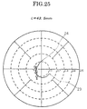
- mag ⁇ means ⁇ 0 in Fig.23
- ⁇ ⁇ means ⁇ in Fig.23.
- These lengths for L are values which are temporarily designed based on the data obtained by the E-O prober.
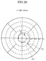
- point 21 in Fig.24 shows the value of ⁇ at 0.5GHz
- point 22 is the value of ⁇ at 1.5GHz.
- ⁇ 1, ⁇ 2 and ⁇ 3 in the figure show the values of ⁇ at interim frequencies 0.9GHz, 1.0GHz and 1.1GHz, respectively.
- points 23 and 25 show the values of ⁇ at 0.5GHz
- points 24 and 26 show the values of ⁇ at 1.5GHz. The following values are based on the measurement values at point ⁇ 2, namely, at 1GHz.
- a precise measurement method for high frequency characteristics, especially for the effective dielectric constant, of the dielectric material is important in developing, designing and estimating a circuit board for a high frequency circuit, since the impedance of a microstrip line is determined by the effective dielectric constant and the line length.
- the measurement method of this invention provides with such a precise measurement method for high frequency characteristics of the dielectric material, leading to its significant effectiveness such that;
- the purpose of this invention is to provide with a method for continuous and accurate measurement of the effective dielectric constant and the dielectric loss of a dielectric material at the same condition as it is implemented in actual circuits.
- Another purpose of this invention is to improve the high frequency circuit design accuracy by providing with a design method using the actual wavelength-shortening ratio of the circuit that is obtained through the measurement of circuit impedance at the same condition as the circuit is practically used.
- the high frequency measurement method for dielectric materials of this invention is characterized as; it measures amplitude and phase variations of the electric field component of an electromagnetic wave along its propagation direction on a high frequency transmission line which is actually implemented as a microstrip line, by using a device whose refraction index changes according to the electric field (or an E-O prober using Pockels Effect), in order to get effective dielectric constant and dielectric loss of said transmission line.
- the high frequency circuit design method of this invention is characterized as; phase variation rate of the electric field component of an electromagnetic wave along its propagation direction on a high frequency transmission line which is actually implemented as a microstrip line is measured by using a device whose refraction index changes according to the electric field (or an E-O prober using Pockels Effect), said phase variation rate is used to derive the wavelength-shortening ratio of said transmission line and said wavelength-shortening ratio is used for the high frequency circuit design.
Landscapes
- Physics & Mathematics (AREA)
- General Physics & Mathematics (AREA)
- Measurement Of Resistance Or Impedance (AREA)
Applications Claiming Priority (2)
| Application Number | Priority Date | Filing Date | Title |
|---|---|---|---|
| JP34874597A JPH11166952A (ja) | 1997-12-04 | 1997-12-04 | 誘電体材料の高周波特性測定方法 |
| JP34874597 | 1997-12-04 |
Publications (2)
| Publication Number | Publication Date |
|---|---|
| EP0921404A2 true EP0921404A2 (fr) | 1999-06-09 |
| EP0921404A3 EP0921404A3 (fr) | 2000-02-23 |
Family
ID=18399091
Family Applications (1)
| Application Number | Title | Priority Date | Filing Date |
|---|---|---|---|
| EP98121710A Withdrawn EP0921404A3 (fr) | 1997-12-04 | 1998-11-13 | Procédé de mesure pour des caractéristiques en hautes fréquences des matériaux diélectriques et procédé de conception des circuits haute fréquence |
Country Status (2)
| Country | Link |
|---|---|
| EP (1) | EP0921404A3 (fr) |
| JP (1) | JPH11166952A (fr) |
Cited By (7)
| Publication number | Priority date | Publication date | Assignee | Title |
|---|---|---|---|---|
| FR2906039A1 (fr) * | 2006-09-20 | 2008-03-21 | Univ Paris Sud Etablissement P | Procede et dispositif pour caracteriser un signal electrique se propageant dans un echantillon. |
| US7701222B2 (en) | 2007-10-19 | 2010-04-20 | International Business Machines Corporation | Method for validating printed circuit board materials for high speed applications |
| DE102014210826A1 (de) * | 2014-06-06 | 2015-12-17 | Conti Temic Microelectronic Gmbh | Prüfverfahren für ein Platinensubstrat und Platine, die insbesondere zur Verwendung in einem solchen Prüfverfahren geeignet ist |
| CN110412436A (zh) * | 2019-07-23 | 2019-11-05 | 大连世有电力科技有限公司 | 基于光电式电压测量的变压器套管介损频谱检测装置 |
| CN111337748A (zh) * | 2020-04-22 | 2020-06-26 | 广西科技大学 | 适用于高温高频条件下的阻抗测量方法 |
| US12078727B2 (en) | 2020-09-14 | 2024-09-03 | Rohde & Schwarz Gmbh & Co. Kg | Imaging system and method for material characterization of a sample |
| CN120652908A (zh) * | 2025-08-19 | 2025-09-16 | 深圳市东一思创电子有限公司 | 射频同轴连接器高频信号传输优化方法 |
Families Citing this family (2)
| Publication number | Priority date | Publication date | Assignee | Title |
|---|---|---|---|---|
| US7649633B2 (en) | 2003-11-20 | 2010-01-19 | National Institute Of Advanced Industrial Science And Technology | Method and instrument for measuring complex dielectric constant of a sample by optical spectral measurement |
| JP7211538B2 (ja) * | 2019-12-20 | 2023-01-24 | 日本電信電話株式会社 | 誘電率測定方法、誘電率測定装置及び誘電率測定プログラム |
Family Cites Families (1)
| Publication number | Priority date | Publication date | Assignee | Title |
|---|---|---|---|---|
| US4603293A (en) * | 1984-03-27 | 1986-07-29 | University Of Rochester | Measurement of electrical signals with subpicosecond resolution |
-
1997
- 1997-12-04 JP JP34874597A patent/JPH11166952A/ja active Pending
-
1998
- 1998-11-13 EP EP98121710A patent/EP0921404A3/fr not_active Withdrawn
Cited By (11)
| Publication number | Priority date | Publication date | Assignee | Title |
|---|---|---|---|---|
| FR2906039A1 (fr) * | 2006-09-20 | 2008-03-21 | Univ Paris Sud Etablissement P | Procede et dispositif pour caracteriser un signal electrique se propageant dans un echantillon. |
| WO2008034962A3 (fr) * | 2006-09-20 | 2008-05-08 | Univ Paris Sud | Procédé et dispositif pour caractériser un signal électrique se propageant dans un échantillon |
| US8421493B2 (en) | 2006-09-20 | 2013-04-16 | Universite Paris Sud | Process and device for characterising an electric signal propagating in a sample |
| US7701222B2 (en) | 2007-10-19 | 2010-04-20 | International Business Machines Corporation | Method for validating printed circuit board materials for high speed applications |
| DE102014210826A1 (de) * | 2014-06-06 | 2015-12-17 | Conti Temic Microelectronic Gmbh | Prüfverfahren für ein Platinensubstrat und Platine, die insbesondere zur Verwendung in einem solchen Prüfverfahren geeignet ist |
| DE102014210826B4 (de) * | 2014-06-06 | 2025-07-03 | Continental Autonomous Mobility Germany GmbH | Prüfverfahren für ein Platinensubstrat und Platine, die insbesondere zur Verwendung in einem solchen Prüfverfahren geeignet ist |
| CN110412436A (zh) * | 2019-07-23 | 2019-11-05 | 大连世有电力科技有限公司 | 基于光电式电压测量的变压器套管介损频谱检测装置 |
| CN111337748A (zh) * | 2020-04-22 | 2020-06-26 | 广西科技大学 | 适用于高温高频条件下的阻抗测量方法 |
| CN111337748B (zh) * | 2020-04-22 | 2022-02-01 | 广西科技大学 | 适用于高温高频条件下的阻抗测量方法 |
| US12078727B2 (en) | 2020-09-14 | 2024-09-03 | Rohde & Schwarz Gmbh & Co. Kg | Imaging system and method for material characterization of a sample |
| CN120652908A (zh) * | 2025-08-19 | 2025-09-16 | 深圳市东一思创电子有限公司 | 射频同轴连接器高频信号传输优化方法 |
Also Published As
| Publication number | Publication date |
|---|---|
| JPH11166952A (ja) | 1999-06-22 |
| EP0921404A3 (fr) | 2000-02-23 |
Similar Documents
| Publication | Publication Date | Title |
|---|---|---|
| EP0160209B1 (fr) | Mesure de signaux électriques avec une résolution inférieure aux picosecondes | |
| Wang et al. | Characterization of dielectric materials at WR-15 band (50–75 GHz) using VNA-based technique | |
| Wang et al. | Broadband printed-circuit-board characterization using multimode substrate-integrated-waveguide resonator | |
| Baker-Jarvis et al. | Dielectric and magnetic measurements: A survey of nondestructive, quasi-nondestructive, and process-control techniques | |
| US10483610B2 (en) | Waveguide mount for microstrip circuit and material characterization | |
| US4745361A (en) | Electro-optic measurement (network analysis) system | |
| Hasar | Permittivity measurement of thin dielectric materials from reflection-only measurements using one-port vector network analyzers | |
| EP0921404A2 (fr) | Procédé de mesure pour des caractéristiques en hautes fréquences des matériaux diélectriques et procédé de conception des circuits haute fréquence | |
| Alexandrou et al. | Time-domain characterization of bent coplanar waveguides | |
| Stanley et al. | Determination of the permittivity of transmission lines at milli-kelvin temperatures | |
| Hasar | Thickness-independent automated constitutive parameters extraction of thin solid and liquid materials from waveguide measurements | |
| US11754605B2 (en) | Series tee splitter for impedance measurements | |
| Deutsch et al. | Characterization of resistive transmission lines to 70 GHz with ultrafast optoelectronics | |
| Yang et al. | High-resolution electro-optic mapping of near-field distributions in integrated microwave circuits | |
| Sahri et al. | Application of 1.55-µm photonic technology to practical millimeter-wave network analysis | |
| US10591530B1 (en) | Coplanar load pull test fixture for wave measurements | |
| KR100732935B1 (ko) | 송신기준 임펄스를 이용한 유전율 측정 프로브 와 측정장치및 그 측정방법 | |
| Hong et al. | Measurement of high-permittivity dielectric characteristics at microwave and mm-wave frequencies | |
| Takahashi et al. | High speed system for measuring electromagnetic field distribution | |
| Kang | Free-Space Material Measurement for a Small Dielectric Plate at W-band | |
| Sequeira | Extracting epsilon and mu of materials from vector reflection measurements | |
| Smith et al. | Spatial field characterization for guided-wave Terahertz sensing | |
| Brown | CHARACTERIZATION AND SIMULATION OF MICROWAVE STRIPLINE DEVICES | |
| JPH11311648A (ja) | 高周波回路の設計方法 | |
| Baker-Jarvis et al. | Dielectric Measurements On Printed-Wiring And Circuit Boards, Thin Films, And Substrates: An Overview1 |
Legal Events
| Date | Code | Title | Description |
|---|---|---|---|
| PUAI | Public reference made under article 153(3) epc to a published international application that has entered the european phase |
Free format text: ORIGINAL CODE: 0009012 |
|
| 17P | Request for examination filed |
Effective date: 19981113 |
|
| AK | Designated contracting states |
Kind code of ref document: A2 Designated state(s): DE GB |
|
| AX | Request for extension of the european patent |
Free format text: AL;LT;LV;MK;RO;SI |
|
| PUAL | Search report despatched |
Free format text: ORIGINAL CODE: 0009013 |
|
| AK | Designated contracting states |
Kind code of ref document: A3 Designated state(s): AT BE CH CY DE DK ES FI FR GB GR IE IT LI LU MC NL PT SE |
|
| AX | Request for extension of the european patent |
Free format text: AL;LT;LV;MK;RO;SI |
|
| AKX | Designation fees paid |
Free format text: DE GB |
|
| STAA | Information on the status of an ep patent application or granted ep patent |
Free format text: STATUS: THE APPLICATION IS DEEMED TO BE WITHDRAWN |
|
| 18D | Application deemed to be withdrawn |
Effective date: 20020603 |