EP0921430A1 - Aktivmatrix-Flüssigkristallanzeige - Google Patents
Aktivmatrix-Flüssigkristallanzeige Download PDFInfo
- Publication number
- EP0921430A1 EP0921430A1 EP98122076A EP98122076A EP0921430A1 EP 0921430 A1 EP0921430 A1 EP 0921430A1 EP 98122076 A EP98122076 A EP 98122076A EP 98122076 A EP98122076 A EP 98122076A EP 0921430 A1 EP0921430 A1 EP 0921430A1
- Authority
- EP
- European Patent Office
- Prior art keywords
- parallel
- electrode
- active matrix
- crystal display
- extending portion
- Prior art date
- Legal status (The legal status is an assumption and is not a legal conclusion. Google has not performed a legal analysis and makes no representation as to the accuracy of the status listed.)
- Granted
Links
- 239000004973 liquid crystal related substance Substances 0.000 title claims abstract description 39
- 239000011159 matrix material Substances 0.000 title claims abstract description 29
- 239000000758 substrate Substances 0.000 claims abstract description 57
- 230000005684 electric field Effects 0.000 claims abstract description 11
- 230000003287 optical effect Effects 0.000 claims description 11
- 239000010408 film Substances 0.000 description 20
- 238000000034 method Methods 0.000 description 18
- 230000000087 stabilizing effect Effects 0.000 description 8
- 238000004519 manufacturing process Methods 0.000 description 7
- 230000004044 response Effects 0.000 description 7
- 230000008569 process Effects 0.000 description 6
- 229910021417 amorphous silicon Inorganic materials 0.000 description 5
- 238000010521 absorption reaction Methods 0.000 description 4
- 230000005669 field effect Effects 0.000 description 4
- 239000010409 thin film Substances 0.000 description 4
- 239000004065 semiconductor Substances 0.000 description 3
- VYZAMTAEIAYCRO-UHFFFAOYSA-N Chromium Chemical compound [Cr] VYZAMTAEIAYCRO-UHFFFAOYSA-N 0.000 description 2
- 229910052581 Si3N4 Inorganic materials 0.000 description 2
- 239000000463 material Substances 0.000 description 2
- 239000000203 mixture Substances 0.000 description 2
- 238000002161 passivation Methods 0.000 description 2
- 230000010287 polarization Effects 0.000 description 2
- HQVNEWCFYHHQES-UHFFFAOYSA-N silicon nitride Chemical compound N12[Si]34N5[Si]62N3[Si]51N64 HQVNEWCFYHHQES-UHFFFAOYSA-N 0.000 description 2
- 230000004075 alteration Effects 0.000 description 1
- 238000010276 construction Methods 0.000 description 1
- 238000007796 conventional method Methods 0.000 description 1
- 239000006185 dispersion Substances 0.000 description 1
- 230000002708 enhancing effect Effects 0.000 description 1
- 230000004048 modification Effects 0.000 description 1
- 238000012986 modification Methods 0.000 description 1
- 238000007789 sealing Methods 0.000 description 1
- 239000003566 sealing material Substances 0.000 description 1
- 230000009466 transformation Effects 0.000 description 1
Images





Classifications
-
- G—PHYSICS
- G02—OPTICS
- G02F—OPTICAL DEVICES OR ARRANGEMENTS FOR THE CONTROL OF LIGHT BY MODIFICATION OF THE OPTICAL PROPERTIES OF THE MEDIA OF THE ELEMENTS INVOLVED THEREIN; NON-LINEAR OPTICS; FREQUENCY-CHANGING OF LIGHT; OPTICAL LOGIC ELEMENTS; OPTICAL ANALOGUE/DIGITAL CONVERTERS
- G02F1/00—Devices or arrangements for the control of the intensity, colour, phase, polarisation or direction of light arriving from an independent light source, e.g. switching, gating or modulating; Non-linear optics
- G02F1/01—Devices or arrangements for the control of the intensity, colour, phase, polarisation or direction of light arriving from an independent light source, e.g. switching, gating or modulating; Non-linear optics for the control of the intensity, phase, polarisation or colour
- G02F1/13—Devices or arrangements for the control of the intensity, colour, phase, polarisation or direction of light arriving from an independent light source, e.g. switching, gating or modulating; Non-linear optics for the control of the intensity, phase, polarisation or colour based on liquid crystals, e.g. single liquid crystal display cells
- G02F1/133—Constructional arrangements; Operation of liquid crystal cells; Circuit arrangements
- G02F1/1333—Constructional arrangements; Manufacturing methods
- G02F1/1343—Electrodes
- G02F1/134309—Electrodes characterised by their geometrical arrangement
- G02F1/134363—Electrodes characterised by their geometrical arrangement for applying an electric field parallel to the substrate, i.e. in-plane switching [IPS]
-
- G—PHYSICS
- G02—OPTICS
- G02F—OPTICAL DEVICES OR ARRANGEMENTS FOR THE CONTROL OF LIGHT BY MODIFICATION OF THE OPTICAL PROPERTIES OF THE MEDIA OF THE ELEMENTS INVOLVED THEREIN; NON-LINEAR OPTICS; FREQUENCY-CHANGING OF LIGHT; OPTICAL LOGIC ELEMENTS; OPTICAL ANALOGUE/DIGITAL CONVERTERS
- G02F1/00—Devices or arrangements for the control of the intensity, colour, phase, polarisation or direction of light arriving from an independent light source, e.g. switching, gating or modulating; Non-linear optics
- G02F1/01—Devices or arrangements for the control of the intensity, colour, phase, polarisation or direction of light arriving from an independent light source, e.g. switching, gating or modulating; Non-linear optics for the control of the intensity, phase, polarisation or colour
- G02F1/13—Devices or arrangements for the control of the intensity, colour, phase, polarisation or direction of light arriving from an independent light source, e.g. switching, gating or modulating; Non-linear optics for the control of the intensity, phase, polarisation or colour based on liquid crystals, e.g. single liquid crystal display cells
- G02F1/133—Constructional arrangements; Operation of liquid crystal cells; Circuit arrangements
- G02F1/136—Liquid crystal cells structurally associated with a semi-conducting layer or substrate, e.g. cells forming part of an integrated circuit
- G02F1/1362—Active matrix addressed cells
- G02F1/136227—Through-hole connection of the pixel electrode to the active element through an insulation layer
-
- G—PHYSICS
- G02—OPTICS
- G02F—OPTICAL DEVICES OR ARRANGEMENTS FOR THE CONTROL OF LIGHT BY MODIFICATION OF THE OPTICAL PROPERTIES OF THE MEDIA OF THE ELEMENTS INVOLVED THEREIN; NON-LINEAR OPTICS; FREQUENCY-CHANGING OF LIGHT; OPTICAL LOGIC ELEMENTS; OPTICAL ANALOGUE/DIGITAL CONVERTERS
- G02F1/00—Devices or arrangements for the control of the intensity, colour, phase, polarisation or direction of light arriving from an independent light source, e.g. switching, gating or modulating; Non-linear optics
- G02F1/01—Devices or arrangements for the control of the intensity, colour, phase, polarisation or direction of light arriving from an independent light source, e.g. switching, gating or modulating; Non-linear optics for the control of the intensity, phase, polarisation or colour
- G02F1/13—Devices or arrangements for the control of the intensity, colour, phase, polarisation or direction of light arriving from an independent light source, e.g. switching, gating or modulating; Non-linear optics for the control of the intensity, phase, polarisation or colour based on liquid crystals, e.g. single liquid crystal display cells
- G02F1/133—Constructional arrangements; Operation of liquid crystal cells; Circuit arrangements
- G02F1/136—Liquid crystal cells structurally associated with a semi-conducting layer or substrate, e.g. cells forming part of an integrated circuit
- G02F1/1362—Active matrix addressed cells
- G02F1/1368—Active matrix addressed cells in which the switching element is a three-electrode device
Definitions
- This invention relates to a liquid-crystal display, and more particularly to, an active matrix liquid-crystal display using lateral electric field drive system.
- An active matrix liquid-crystal display where thin film field-effect transistor (TFT) is used as a switching element of pixel has a high image quality, and is wide used as a display device of portable computer or recently a monitor for space-saving type desktop computer.
- TFT thin film field-effect transistor
- a display system using the lateral electric field is proposed.
- This system is, for example, disclosed in Japanese patent application laid-open No.6-160878 (1994).
- a pixel electrode and an opposing electrode are formed parallel on a same substrate, a voltage is applied between them to form parallel field on the surface of the substrate, thereby the direction of anisotropic axis (liquid-crystal director) of liquid crystal (hereinafter also referred to as 'LC') is varied, thereby the amount of transmitted light is controlled.
- 7 is a LC director
- 8 is an emission-side polarizing plate
- 10 is a transparent insulative substrate
- 11 is orientation film
- 12 is an incidence-side polarizing plate
- 18 is transparent conductive film
- 21 is a dividing boundary.
- Japanese patent publication No.59-7367 (1984) discloses the method that, as shown in FIG.2, LC with positive permittivity anisotropy is vertically oriented and LC director 7 is inclined by applying lateral field through comb-like electrode 24 formed on a transparent insulative substrate 10. Also in this method, for the purpose of determining uniquely the inclining direction of LC, it is necessary to incline, in advance, the orientation direction of LC to either side, because there exist two inclining directions of LC when LC is completely vertically oriented.
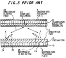
- Japanese patent application laid-open No.56-88179 (1981) discloses a method where comb-like electrodes 24 are formed on both sides of a transparent insulative substrate 10 as shown in FIG.3.
- the direction of electric field occurring when a voltage is applied to the comb-like electrode 24 is oblique.
- the oblique electric field 22 generates in two directions and therefore LC oriented vertically is inclined in the two directions.
- the precision of overlapping is worse than that of the case that both are formed on a same substrate. Therefore, it is difficult to reduce the dispersion of electrode intervals and high-precision LC cell cannot be produced.
- an object of the invention to provide an active matrix liquid-crystal display which has a good view-angle characteristic, excellent response characteristic and reliability.
- an active matrix liquid-crystal display comprises:
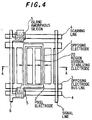
- FIG.4 is a plan view showing one pixel of an active matrix liquid-crystal display in the first embodiment of the invention.
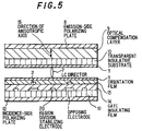
- FIG.5 is a cross sectional view cut along the line A-A in FIG.4.
- the active matrix liquid-crystal display of the invention is composed of two transparent insulative substrates 10. Disposed on one transparent insulative substrate 10 are several scanning lines 4, several signal lines 6 formed in the direction of intersecting the scanning line 4, and several switching elements (thin-film field-effect transistors) formed near the intersecting point of the scanning line 4 and signal line 6. Also, a pixel electrode 2 connected to each switching element is formed, through gate insulating film 14, above a wider opposing electrode 1 than this.
- each pixel electrode 2 is connected to the thin-film field-effect transistor with an island amorphous silicon 5 as a semiconductor layer and the scanning line 4 as a gate.
- the scanning line 4 is turn on, a potential of the signal line 6 can be written.
- An alternating-current voltage can be applied between this and the opposing electrode 1 which is kept a constant potential by an opposing electrode bus line 3.
- region division stabilizing electrodes 20 extending parallel, with an interval, to the opposing electrode 1 just under the pixel electrode 2 are formed.
- orientation film 11 is disposed outside passivation film 13 formed on one transparent insulative substrate 10.
- optical compensation layer 9 is formed on another transparent insulative substrate 10
- an emission-side polarizing plate 8 is formed on this optical compensation layer 9, and orientation film 11 is formed on the outer surface of the transparent insulative substrate 10.
- LC is disposed between both the transparent insulative substrates 10. LC has positive permittivity anisotropy, and is oriented nearly vertically to both the transparent insulative substrates 10.
- An incidence-side polarizing plate 12 outside one transparent insulative substrate 10 and the emission-side polarizing plate 8 outside another transparent insulative substrate 10 are disposed in crossed-Nicol state.
- the polarization axis of the incidence-side polarizing plate 12 is made to be 45° to the longitudinal direction of the pixel electrode 2 shown in FIG.4.
- the absorption axis of the incidence-side polarizing plate 12 is made to be along the rubbing direction, and the absorption axis of the emission-side polarizing plate 8 is made to be perpendicular to the rubbing direction.
- refractive-index anisotropy when viewing from the front surface, refractive-index anisotropy generates in the direction of inclining LC, i.e., in the direction of 45° to the polarization axis to form the crossed-Nicol.
- retardation to the transmitted light of the incidence-side polarizing plate 12 occurs in the LC layer, thereby the permittivity is increased.
- the inclining angle of LC can be controlled by controlling the applied voltage. Therefore, the amount of transmitted light can be controlled by the voltage.
- the inclining directions of LC director 7 at both sides of the pixel electrode 2 are separated into two directions that are 180° different from each other. If it inclines in only one direction, when viewing obliquely the transparent insulative substrate 10 from the inclining direction of LC, tone inversion etc. occurs and the view angle is narrowed. In contrast to this, when LC's are inclined in the two directions as in the first embodiment of the invention, due to the two regions compensating each other, the occurrence of tone inversion becomes hard and the view-angle characteristic becomes good.
- an active matrix substrate with such a pixel composition as shown in FIG.4 will be prepared.
- Chrome film of 150nm thick is deposited on the transparent insulative substrate 10, and then it is patterned into a shape to form the linear opposing electrode 1, linear electrode 20 for stabilizing the region division to be connected with the opposing electrode 1, scanning line 4, and opposing electrode bus line 3.
- silicon nitride film of 400nm as gate insulating film 14 amorphous silicon film of 350nm as semiconductor layer, and n-type amorphous silicon film of 30nm are deposited, and then the amorphous silicon film is patterned into the island shape 5.
- chrome film of 150nm is deposited, and then it is patterned into a shape to form the signal line 6 and pixel electrode 2.
- 200nm thick silicon nitride film as the passivation film 13 is deposited, and is patterned to expose the terminal electrode.
- the width of pixel electrode 2 is 4 ⁇ m, and the opposing electrode 1 disposed under the pixel electrode 2 is 8 ⁇ m in width, wider than by 2 ⁇ m at both sides thereof.
- the width of linear electrode 20 for stabilizing the region division, which is connected to the opposing electrode 1, to be formed near the center of two adjacent pixel electrodes 2 is 4 ⁇ m.
- orientation films 11 that LC to contact these is perpendicularly oriented are coated respectively. These are bonded, fixing the fringe with a sealing material, filling LC into this, sealing it.
- the LC cell gap dLC is 5.5 ⁇ m.
- the refractive-index anisotropy ⁇ nLC of LC filled is 0.075.
- the direction of LC director 7 is oriented perpendicularly to the substrate (transparent insulative substrate 10).
- the optical compensation layer 9 is formed outside the opposing substrate (transparent insulative substrate 10).
- the optical compensation layer 9 has negative uniaxial refractive-index anisotropy, where the direction of refractive-index anisotropic axis is made perpendicular to the transparent insulative substrate 10.
- the product, ⁇ nF ⁇ dF, of the refractive-index anisotropy ⁇ nF and thickness dF in the optical compensation layer 9 is 165nm.
- the absorption axis of the incidence-side polarizing plate 12 is directed in the direction of 45° to the longitudinal direction of pixel electrode 2, and the absorption axis of the emission-side polarizing plate 8 is directed perpendicularly to this.
- the LC display panel fabricated as described above is normally black and presents a good front display characteristic. Also, the view angle characteristic is very good. Also, the response is fast and a good image can be obtained even in movie display.
- the pixel electrode 2 is composed of single or several linear electrodes, the wider linear opposing electrode 1 than the pixel electrode 2 is formed through the gate insulating film 14.
- the direction of LC oriented perpendicularly to the transparent insulative substrate 10 is controlled.
- the optical compensation layer 9 with negative uniaxial refractive-index anisotropy in the normal-line direction of the substrate between the other transparent insulative substrate 10 and emission-side polarizing plate 8, the white floatation caused by that LC layer has retardation in black display state, i.e., perpendicular orientation state, can be suppressed.
- LC's are inclined in different directions 17 on both sides of pixel electrode 2, and therefore a boundary 16 occurs in a region where LC's are inclined in the reverse direction each other near the center thereof.
- this boundary 16 may be discrimination and may cause the display non-uniformity or residual image.
- it is effective to form the linear electrode (region division stabilizing electrode) 20 for stabilizing the region division, which is connected to the opposing electrode 1, near the center of two adjacent pixel electrodes 2.
- the optical compensation layer 9 is disposed between the emission-side polarizing plate 8 and the other transparent insulative substrate 10. However, it can be disposed separately between the emission-side polarizing plate 8 and the other transparent insulative substrate 10, and between the incidence-side polarizing plate 12 and one transparent insulative substrate 10, thereby making the sum of both retardation equal to the retardation of LC.
- LC is oriented nearly perpendicular to the substrate.
- LC director 7 is inclined in the longitudinal direction of the signal line 6.
- the extending direction of pixel electrode 2 is made parallel to the signal line 6.
- it can be parallel to the scanning line 4.
- the fabrication method is similar to that explained above in the first embodiment.
- the quality of image is on nearly same level.
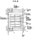
- FIG.9 is a plan view showing one pixel of an active matrix liquid-crystal display in the second embodiment of the invention.
- the pixel electrode 2 is formed, through the gate insulating film 14, over the wider opposing electrode 1 than this.
- Each pixel electrode 2 is connected to the thin-film field-effect transistor with an island amorphous silicon 5 as a semiconductor layer and the scanning line 4 as a gate.
- the scanning line 4 is turn on, a potential of the signal line 6 can be written.
- An alternating-current voltage can be applied between this and the opposing electrode 1 which is kept a constant potential by an opposing electrode bus line 3.
- region division stabilizing electrodes 20 extending parallel, with an interval, to the opposing electrode 1 just under the pixel electrode 2 are formed.
- the pixel electrode 2 has a parallel extending portion 2a extending parallel to the signal line 6 and a orthogonal extending portion 2b (portion extending parallel to the scanning line 4) extending in the orthogonal direction of the parallel extending portion 2a.
- the other composition is the same as that in the first embodiment described earlier.
- directions where LC's are to be inclined by voltage application are, in total, four, of the pixel electrode 2, two directions perpendicularly to the parallel extending portion 2a extending parallel to the signal line 6 and two directions perpendicularly to the portion extending parallel to the scanning line 4, i.e., the orthogonal extending portion 2b.
- LC's inclined to these four directions are compensated each other, and therefore the view angle can be better than that in the first embodiment.
- the fabrication method of the second embodiment is the same as that of the first embodiment.
- an active matrix substrate with pixel structure shown in FIG.9 is fabricated.
- the width of pixel electrode 2 is 4 ⁇ m
- the opposing electrode 1 disposed under the pixel electrode 2 is 8 ⁇ m in width, wider than by 2 ⁇ m at both sides thereof.
- the width of linear electrode 20 for stabilizing the region division, which is connected to the opposing electrode 1, to be formed near the center of two adjacent pixel electrodes 2 is 4 ⁇ m.
- the fabrication process following below is the same as that in the first embodiment.
- the LC display panel fabricated as described above is normally black and presents a good front display characteristic. Also, the view angle characteristic is better than that of the LC display in the first embodiment. Also, the response is fast and a good image can be obtained even in movie display.
- the optical compensation layer 9 is disposed between the emission-side polarizing plate 8 and the other transparent insulative substrate 10. However, it can be disposed separately between the incidence-side polarizing plate 12 and one transparent insulative substrate 10-1. Also, it can be disposed separately between the emission-side polarizing plate 8 and the other transparent insulative substrate 10-2 and between the incidence-side polarizing plate 12 and one transparent insulative substrate 10-1, thereby making the sum of both retardation equal to the retardation of LC.
- the liquid-crystal layer is perpendicularly oriented and LC's on both sides of pixel electrode are inclined in two directions of 180° different each other by a voltage applied between a wide opposing electrode and a pixel electrode disposed over the opposing electrode.
Landscapes
- Physics & Mathematics (AREA)
- Nonlinear Science (AREA)
- General Physics & Mathematics (AREA)
- Chemical & Material Sciences (AREA)
- Crystallography & Structural Chemistry (AREA)
- Mathematical Physics (AREA)
- Optics & Photonics (AREA)
- Geometry (AREA)
- Engineering & Computer Science (AREA)
- Microelectronics & Electronic Packaging (AREA)
- Liquid Crystal (AREA)
- Thin Film Transistor (AREA)
- Devices For Indicating Variable Information By Combining Individual Elements (AREA)
Applications Claiming Priority (2)
| Application Number | Priority Date | Filing Date | Title |
|---|---|---|---|
| JP9320121A JP3031317B2 (ja) | 1997-11-20 | 1997-11-20 | アクティブマトリクス液晶表示装置 |
| JP32012197 | 1997-11-20 |
Publications (2)
| Publication Number | Publication Date |
|---|---|
| EP0921430A1 true EP0921430A1 (de) | 1999-06-09 |
| EP0921430B1 EP0921430B1 (de) | 2006-04-12 |
Family
ID=18117938
Family Applications (1)
| Application Number | Title | Priority Date | Filing Date |
|---|---|---|---|
| EP98122076A Expired - Lifetime EP0921430B1 (de) | 1997-11-20 | 1998-11-20 | Aktivmatrix-Flüssigkristallanzeige |
Country Status (5)
| Country | Link |
|---|---|
| US (1) | US6052168A (de) |
| EP (1) | EP0921430B1 (de) |
| JP (1) | JP3031317B2 (de) |
| KR (1) | KR100314697B1 (de) |
| DE (1) | DE69834164T2 (de) |
Cited By (1)
| Publication number | Priority date | Publication date | Assignee | Title |
|---|---|---|---|---|
| EP2051135A4 (de) * | 2006-08-08 | 2010-06-16 | Sharp Kk | Tft-substrat, flüssigkristallanzeigeschirm und flüssigkristallanzeigeanordnung mit dem substrat und verfahren zur herstellung eines tft-substrats |
Families Citing this family (19)
| Publication number | Priority date | Publication date | Assignee | Title |
|---|---|---|---|---|
| JP2991995B2 (ja) * | 1997-07-14 | 1999-12-20 | 三菱電機株式会社 | 液晶表示装置 |
| JP3479696B2 (ja) * | 1997-12-08 | 2003-12-15 | ビオイ−ハイディス テクノロジー カンパニー リミテッド | 液晶表示装置 |
| TW451099B (en) * | 1998-01-23 | 2001-08-21 | Hitachi Ltd | Liquid crystal display device |
| JP2982869B2 (ja) * | 1998-04-16 | 1999-11-29 | インターナショナル・ビジネス・マシーンズ・コーポレイション | 液晶表示装置 |
| KR100306799B1 (ko) * | 1998-05-29 | 2001-11-30 | 박종섭 | 액정표시장치 |
| JP3129293B2 (ja) | 1998-08-13 | 2001-01-29 | 日本電気株式会社 | 液晶表示装置 |
| JP3957430B2 (ja) * | 1998-09-18 | 2007-08-15 | シャープ株式会社 | 液晶表示装置 |
| US6642984B1 (en) * | 1998-12-08 | 2003-11-04 | Fujitsu Display Technologies Corporation | Liquid crystal display apparatus having wide transparent electrode and stripe electrodes |
| US6762816B1 (en) * | 1999-06-11 | 2004-07-13 | Matsushita Electric Industrial Co., Ltd. | Liquid crystal display with special electrode configurations and compositions and method for producing the same |
| JP3481509B2 (ja) * | 1999-06-16 | 2003-12-22 | Nec液晶テクノロジー株式会社 | 液晶表示装置 |
| US6636289B2 (en) * | 2000-04-19 | 2003-10-21 | Lg.Philips Lcd Co., Ltd. | In-plane switching LCD panel with multiple domains and rubbing directions symetric about a line |
| KR100587367B1 (ko) * | 2000-10-20 | 2006-06-08 | 엘지.필립스 엘시디 주식회사 | 횡전계방식 액정표시장치 및 그 제조방법 |
| US6669520B2 (en) * | 2001-09-19 | 2003-12-30 | United Microelectronics Corp. | Method of fabricating an LC panel |
| KR100895017B1 (ko) * | 2002-12-10 | 2009-04-30 | 엘지디스플레이 주식회사 | 개구율이 향상된 횡전계모드 액정표시소자 |
| JP3864929B2 (ja) * | 2003-04-15 | 2007-01-10 | ソニー株式会社 | 液晶表示素子、画像表示装置 |
| US7564510B2 (en) * | 2004-01-26 | 2009-07-21 | Sharp Kabushiki Kaisha | Liquid crystal display device and method for driving the same |
| JP5477523B2 (ja) * | 2006-06-15 | 2014-04-23 | 三国電子有限会社 | 低コスト大画面広視野角高速応答液晶表示装置 |
| JP5426823B2 (ja) * | 2007-11-06 | 2014-02-26 | エルジー ディスプレイ カンパニー リミテッド | 液晶表示装置 |
| WO2012086666A1 (ja) * | 2010-12-22 | 2012-06-28 | シャープ株式会社 | 液晶パネルおよび液晶表示装置 |
Citations (3)
| Publication number | Priority date | Publication date | Assignee | Title |
|---|---|---|---|---|
| JPH06202073A (ja) * | 1992-12-28 | 1994-07-22 | Hitachi Ltd | アクティブマトリクス型液晶表示装置 |
| JPH09197420A (ja) * | 1996-01-12 | 1997-07-31 | Nec Corp | 液晶素子 |
| EP0805374A2 (de) * | 1996-05-01 | 1997-11-05 | Stanley Electric Co., Ltd. | Flüssigkristall-Anzeigevorrichtung vom horizontalen Feldtyp |
Family Cites Families (8)
| Publication number | Priority date | Publication date | Assignee | Title |
|---|---|---|---|---|
| JPS5688179A (en) * | 1979-12-20 | 1981-07-17 | Tokyo Shibaura Electric Co | Color liquiddcrystal display unit |
| JPS597367B2 (ja) * | 1981-04-27 | 1984-02-17 | シャープ株式会社 | 電界効果型液晶表示装置 |
| JPS597367A (ja) * | 1982-07-05 | 1984-01-14 | Fuji Xerox Co Ltd | 電子写真用透明フイルム |
| JP2940354B2 (ja) * | 1992-09-18 | 1999-08-25 | 株式会社日立製作所 | 液晶表示装置 |
| US5504603A (en) * | 1994-04-04 | 1996-04-02 | Rockwell International Corporation | Optical compensator for improved gray scale performance in liquid crystal display |
| JP3396130B2 (ja) * | 1996-06-03 | 2003-04-14 | シャープ株式会社 | 液晶表示装置 |
| JPH1026765A (ja) * | 1996-07-10 | 1998-01-27 | Toshiba Corp | 液晶表示素子、投影型液晶表示装置及び基板 |
| JPH10186351A (ja) * | 1996-12-24 | 1998-07-14 | Hitachi Ltd | 液晶表示装置 |
-
1997
- 1997-11-20 JP JP9320121A patent/JP3031317B2/ja not_active Expired - Lifetime
-
1998
- 1998-11-19 US US09/195,618 patent/US6052168A/en not_active Expired - Lifetime
- 1998-11-20 EP EP98122076A patent/EP0921430B1/de not_active Expired - Lifetime
- 1998-11-20 KR KR1019980049875A patent/KR100314697B1/ko not_active Expired - Fee Related
- 1998-11-20 DE DE69834164T patent/DE69834164T2/de not_active Expired - Lifetime
Patent Citations (3)
| Publication number | Priority date | Publication date | Assignee | Title |
|---|---|---|---|---|
| JPH06202073A (ja) * | 1992-12-28 | 1994-07-22 | Hitachi Ltd | アクティブマトリクス型液晶表示装置 |
| JPH09197420A (ja) * | 1996-01-12 | 1997-07-31 | Nec Corp | 液晶素子 |
| EP0805374A2 (de) * | 1996-05-01 | 1997-11-05 | Stanley Electric Co., Ltd. | Flüssigkristall-Anzeigevorrichtung vom horizontalen Feldtyp |
Non-Patent Citations (2)
| Title |
|---|
| PATENT ABSTRACTS OF JAPAN vol. 018, no. 557 (P - 1817) 24 October 1994 (1994-10-24) * |
| PATENT ABSTRACTS OF JAPAN vol. 097, no. 011 28 November 1997 (1997-11-28) * |
Cited By (1)
| Publication number | Priority date | Publication date | Assignee | Title |
|---|---|---|---|---|
| EP2051135A4 (de) * | 2006-08-08 | 2010-06-16 | Sharp Kk | Tft-substrat, flüssigkristallanzeigeschirm und flüssigkristallanzeigeanordnung mit dem substrat und verfahren zur herstellung eines tft-substrats |
Also Published As
| Publication number | Publication date |
|---|---|
| JPH11153802A (ja) | 1999-06-08 |
| US6052168A (en) | 2000-04-18 |
| KR19990045445A (ko) | 1999-06-25 |
| JP3031317B2 (ja) | 2000-04-10 |
| EP0921430B1 (de) | 2006-04-12 |
| KR100314697B1 (ko) | 2002-10-25 |
| DE69834164T2 (de) | 2007-01-25 |
| DE69834164D1 (de) | 2006-05-24 |
Similar Documents
| Publication | Publication Date | Title |
|---|---|---|
| EP0921430B1 (de) | Aktivmatrix-Flüssigkristallanzeige | |
| US6750934B2 (en) | Active-matrix liquid crystal display | |
| KR100359352B1 (ko) | 액정 표시 장치 및 그 제조 방법 | |
| EP0916992B1 (de) | Flüssigkristall-Anzeigevorrichtung | |
| KR100246980B1 (ko) | 액티브 매트릭스형 액정표시소자 | |
| US7474292B2 (en) | Liquid crystal display device | |
| US20070200990A1 (en) | Liquid crystal display device | |
| JP4287628B2 (ja) | 液晶表示装置および液晶表示装置の製造方法 | |
| JP3234357B2 (ja) | 液晶表示装置 | |
| JP2002182230A (ja) | フリンジフィールドスイッチングモード液晶表示装置 | |
| JPH06273803A (ja) | アクティブマトリクス型液晶表示装置 | |
| US6784967B2 (en) | In-plane switching LCD device having slanted corner portions | |
| KR20040002156A (ko) | 수직 배향 모드 액정표시장치 | |
| US20010043301A1 (en) | Structure of a multi-domain wide viewing angle liquid crystal display | |
| JP3039517B2 (ja) | アクティブマトリクス液晶表示装置 | |
| US20020018156A1 (en) | In-plane switching LCD device | |
| KR100781477B1 (ko) | 액정 표시 장치 | |
| JP2856188B2 (ja) | アクティブマトリクス液晶表示パネル | |
| US7499138B2 (en) | Panel and a liquid crystal display including the panel | |
| US20040239856A1 (en) | Liquid crystal display device | |
| JPH05232474A (ja) | 液晶表示素子 | |
| JPH11174462A (ja) | 液晶表示素子 | |
| US6573966B1 (en) | Parallel field device with compensating domains held by a boundary surface and stabilized by auxiliary electrodes | |
| KR100709700B1 (ko) | 액정 표시 장치 및 액정 표시 장치용 기판 | |
| KR20010096155A (ko) | 액정 표시 장치 |
Legal Events
| Date | Code | Title | Description |
|---|---|---|---|
| PUAI | Public reference made under article 153(3) epc to a published international application that has entered the european phase |
Free format text: ORIGINAL CODE: 0009012 |
|
| 17P | Request for examination filed |
Effective date: 19990308 |
|
| AK | Designated contracting states |
Kind code of ref document: A1 Designated state(s): DE FR GB |
|
| AX | Request for extension of the european patent |
Free format text: AL;LT;LV;MK;RO;SI |
|
| AKX | Designation fees paid |
Free format text: DE FR GB |
|
| RAP1 | Party data changed (applicant data changed or rights of an application transferred) |
Owner name: NEC LCD TECHNOLOGIES, LTD. |
|
| GRAP | Despatch of communication of intention to grant a patent |
Free format text: ORIGINAL CODE: EPIDOSNIGR1 |
|
| GRAS | Grant fee paid |
Free format text: ORIGINAL CODE: EPIDOSNIGR3 |
|
| GRAA | (expected) grant |
Free format text: ORIGINAL CODE: 0009210 |
|
| AK | Designated contracting states |
Kind code of ref document: B1 Designated state(s): DE FR GB |
|
| REG | Reference to a national code |
Ref country code: GB Ref legal event code: FG4D |
|
| REF | Corresponds to: |
Ref document number: 69834164 Country of ref document: DE Date of ref document: 20060524 Kind code of ref document: P |
|
| PLBE | No opposition filed within time limit |
Free format text: ORIGINAL CODE: 0009261 |
|
| STAA | Information on the status of an ep patent application or granted ep patent |
Free format text: STATUS: NO OPPOSITION FILED WITHIN TIME LIMIT |
|
| 26N | No opposition filed |
Effective date: 20070115 |
|
| EN | Fr: translation not filed | ||
| PG25 | Lapsed in a contracting state [announced via postgrant information from national office to epo] |
Ref country code: FR Free format text: LAPSE BECAUSE OF FAILURE TO SUBMIT A TRANSLATION OF THE DESCRIPTION OR TO PAY THE FEE WITHIN THE PRESCRIBED TIME-LIMIT Effective date: 20070309 |
|
| PG25 | Lapsed in a contracting state [announced via postgrant information from national office to epo] |
Ref country code: FR Free format text: LAPSE BECAUSE OF FAILURE TO SUBMIT A TRANSLATION OF THE DESCRIPTION OR TO PAY THE FEE WITHIN THE PRESCRIBED TIME-LIMIT Effective date: 20060412 |
|
| REG | Reference to a national code |
Ref country code: DE Ref legal event code: R082 Ref document number: 69834164 Country of ref document: DE Representative=s name: GLAWE DELFS MOLL PARTNERSCHAFT MBB VON PATENT-, DE Effective date: 20110919 Ref country code: DE Ref legal event code: R081 Ref document number: 69834164 Country of ref document: DE Owner name: NLT TECHNOLOGIES, LTD., KAWASAKI, JP Free format text: FORMER OWNER: NEC LCD TECHNOLOGIES, LTD., KAWASAKI, KANAGAWA, JP Effective date: 20110919 |
|
| PGFP | Annual fee paid to national office [announced via postgrant information from national office to epo] |
Ref country code: DE Payment date: 20171121 Year of fee payment: 20 |
|
| PGFP | Annual fee paid to national office [announced via postgrant information from national office to epo] |
Ref country code: GB Payment date: 20171123 Year of fee payment: 20 |
|
| REG | Reference to a national code |
Ref country code: DE Ref legal event code: R071 Ref document number: 69834164 Country of ref document: DE |
|
| REG | Reference to a national code |
Ref country code: GB Ref legal event code: PE20 Expiry date: 20181119 |
|
| PG25 | Lapsed in a contracting state [announced via postgrant information from national office to epo] |
Ref country code: GB Free format text: LAPSE BECAUSE OF EXPIRATION OF PROTECTION Effective date: 20181119 |