EP0921579A2 - Dünfilmtransistor basierend auf substituierten Phthalocyaninen - Google Patents
Dünfilmtransistor basierend auf substituierten Phthalocyaninen Download PDFInfo
- Publication number
- EP0921579A2 EP0921579A2 EP98309580A EP98309580A EP0921579A2 EP 0921579 A2 EP0921579 A2 EP 0921579A2 EP 98309580 A EP98309580 A EP 98309580A EP 98309580 A EP98309580 A EP 98309580A EP 0921579 A2 EP0921579 A2 EP 0921579A2
- Authority
- EP
- European Patent Office
- Prior art keywords
- phthalocyanine
- layer
- substrate
- thin film
- substituted
- Prior art date
- Legal status (The legal status is an assumption and is not a legal conclusion. Google has not performed a legal analysis and makes no representation as to the accuracy of the status listed.)
- Withdrawn
Links
- 239000010409 thin film Substances 0.000 title claims abstract description 13
- 239000000758 substrate Substances 0.000 claims abstract description 63
- IEQIEDJGQAUEQZ-UHFFFAOYSA-N phthalocyanine Chemical class N1C(N=C2C3=CC=CC=C3C(N=C3C4=CC=CC=C4C(=N4)N3)=N2)=C(C=CC=C2)C2=C1N=C1C2=CC=CC=C2C4=N1 IEQIEDJGQAUEQZ-UHFFFAOYSA-N 0.000 claims abstract description 51
- 150000001875 compounds Chemical class 0.000 claims abstract description 36
- 230000005669 field effect Effects 0.000 claims abstract description 29
- HCHKCACWOHOZIP-UHFFFAOYSA-N Zinc Chemical compound [Zn] HCHKCACWOHOZIP-UHFFFAOYSA-N 0.000 claims abstract description 7
- 229910052725 zinc Inorganic materials 0.000 claims abstract description 7
- 239000011701 zinc Substances 0.000 claims abstract description 7
- PXGOKWXKJXAPGV-UHFFFAOYSA-N Fluorine Chemical compound FF PXGOKWXKJXAPGV-UHFFFAOYSA-N 0.000 claims abstract description 5
- 229910052731 fluorine Inorganic materials 0.000 claims abstract description 5
- 239000011737 fluorine Substances 0.000 claims abstract description 5
- 239000004065 semiconductor Substances 0.000 claims description 40
- 239000010949 copper Substances 0.000 claims description 16
- RYGMFSIKBFXOCR-UHFFFAOYSA-N Copper Chemical group [Cu] RYGMFSIKBFXOCR-UHFFFAOYSA-N 0.000 claims description 15
- XEEYBQQBJWHFJM-UHFFFAOYSA-N Iron Chemical group [Fe] XEEYBQQBJWHFJM-UHFFFAOYSA-N 0.000 claims description 15
- 229910052802 copper Inorganic materials 0.000 claims description 15
- 229910052742 iron Inorganic materials 0.000 claims description 7
- 239000000460 chlorine Substances 0.000 claims description 6
- ZAMOUSCENKQFHK-UHFFFAOYSA-N Chlorine atom Chemical compound [Cl] ZAMOUSCENKQFHK-UHFFFAOYSA-N 0.000 claims description 4
- 229910052801 chlorine Inorganic materials 0.000 claims description 4
- 125000006575 electron-withdrawing group Chemical group 0.000 claims description 3
- 125000001424 substituent group Chemical group 0.000 claims 2
- 239000000463 material Substances 0.000 abstract description 55
- 239000010408 film Substances 0.000 abstract description 42
- 238000000034 method Methods 0.000 abstract description 12
- ATJFFYVFTNAWJD-UHFFFAOYSA-N Tin Chemical compound [Sn] ATJFFYVFTNAWJD-UHFFFAOYSA-N 0.000 abstract description 3
- RBTKNAXYKSUFRK-UHFFFAOYSA-N heliogen blue Chemical compound [Cu].[N-]1C2=C(C=CC=C3)C3=C1N=C([N-]1)C3=CC=CC=C3C1=NC([N-]1)=C(C=CC=C3)C3=C1N=C([N-]1)C3=CC=CC=C3C1=N2 RBTKNAXYKSUFRK-UHFFFAOYSA-N 0.000 abstract description 3
- 229910052739 hydrogen Inorganic materials 0.000 abstract description 3
- 239000001257 hydrogen Substances 0.000 abstract description 3
- 229910052718 tin Inorganic materials 0.000 abstract description 3
- 125000001309 chloro group Chemical group Cl* 0.000 abstract description 2
- 125000004435 hydrogen atom Chemical class [H]* 0.000 abstract description 2
- 230000037230 mobility Effects 0.000 description 59
- 229910052751 metal Inorganic materials 0.000 description 16
- 239000002184 metal Substances 0.000 description 16
- 229910052710 silicon Inorganic materials 0.000 description 8
- 239000010703 silicon Substances 0.000 description 8
- VYPSYNLAJGMNEJ-UHFFFAOYSA-N Silicium dioxide Chemical compound O=[Si]=O VYPSYNLAJGMNEJ-UHFFFAOYSA-N 0.000 description 6
- XUIMIQQOPSSXEZ-UHFFFAOYSA-N Silicon Chemical compound [Si] XUIMIQQOPSSXEZ-UHFFFAOYSA-N 0.000 description 6
- 238000000151 deposition Methods 0.000 description 5
- 230000008021 deposition Effects 0.000 description 5
- 239000003989 dielectric material Substances 0.000 description 5
- 230000000694 effects Effects 0.000 description 5
- PCHJSUWPFVWCPO-UHFFFAOYSA-N gold Chemical compound [Au] PCHJSUWPFVWCPO-UHFFFAOYSA-N 0.000 description 5
- 229910052737 gold Inorganic materials 0.000 description 5
- 239000010931 gold Substances 0.000 description 5
- 239000011521 glass Substances 0.000 description 4
- -1 gold) Chemical class 0.000 description 4
- 230000005525 hole transport Effects 0.000 description 4
- 229920003023 plastic Polymers 0.000 description 4
- BASFCYQUMIYNBI-UHFFFAOYSA-N platinum Chemical compound [Pt] BASFCYQUMIYNBI-UHFFFAOYSA-N 0.000 description 4
- 229920006395 saturated elastomer Polymers 0.000 description 4
- PXHVJJICTQNCMI-UHFFFAOYSA-N Nickel Chemical compound [Ni] PXHVJJICTQNCMI-UHFFFAOYSA-N 0.000 description 3
- 230000015572 biosynthetic process Effects 0.000 description 3
- 230000007423 decrease Effects 0.000 description 3
- FJAOBQORBYMRNO-UHFFFAOYSA-N f16cupc Chemical compound [Cu+2].[N-]1C(N=C2C3=C(F)C(F)=C(F)C(F)=C3C(N=C3C4=C(F)C(F)=C(F)C(F)=C4C(=N4)[N-]3)=N2)=C(C(F)=C(F)C(F)=C2F)C2=C1N=C1C2=C(F)C(F)=C(F)C(F)=C2C4=N1 FJAOBQORBYMRNO-UHFFFAOYSA-N 0.000 description 3
- 150000002500 ions Chemical class 0.000 description 3
- 235000012239 silicon dioxide Nutrition 0.000 description 3
- 239000000377 silicon dioxide Substances 0.000 description 3
- 230000008022 sublimation Effects 0.000 description 3
- 238000000859 sublimation Methods 0.000 description 3
- 239000011135 tin Substances 0.000 description 3
- 238000001771 vacuum deposition Methods 0.000 description 3
- OPFJDXRVMFKJJO-ZHHKINOHSA-N N-{[3-(2-benzamido-4-methyl-1,3-thiazol-5-yl)-pyrazol-5-yl]carbonyl}-G-dR-G-dD-dD-dD-NH2 Chemical compound S1C(C=2NN=C(C=2)C(=O)NCC(=O)N[C@H](CCCN=C(N)N)C(=O)NCC(=O)N[C@H](CC(O)=O)C(=O)N[C@H](CC(O)=O)C(=O)N[C@H](CC(O)=O)C(N)=O)=C(C)N=C1NC(=O)C1=CC=CC=C1 OPFJDXRVMFKJJO-ZHHKINOHSA-N 0.000 description 2
- KYQCOXFCLRTKLS-UHFFFAOYSA-N Pyrazine Chemical compound C1=CN=CC=N1 KYQCOXFCLRTKLS-UHFFFAOYSA-N 0.000 description 2
- 229910052581 Si3N4 Inorganic materials 0.000 description 2
- 238000002441 X-ray diffraction Methods 0.000 description 2
- 229910052782 aluminium Inorganic materials 0.000 description 2
- XAGFODPZIPBFFR-UHFFFAOYSA-N aluminium Chemical compound [Al] XAGFODPZIPBFFR-UHFFFAOYSA-N 0.000 description 2
- 229940126086 compound 21 Drugs 0.000 description 2
- 238000007796 conventional method Methods 0.000 description 2
- 230000008020 evaporation Effects 0.000 description 2
- 238000001704 evaporation Methods 0.000 description 2
- TWNQGVIAIRXVLR-UHFFFAOYSA-N oxo(oxoalumanyloxy)alumane Chemical compound O=[Al]O[Al]=O TWNQGVIAIRXVLR-UHFFFAOYSA-N 0.000 description 2
- 239000004033 plastic Substances 0.000 description 2
- 229910052697 platinum Inorganic materials 0.000 description 2
- 150000003376 silicon Chemical class 0.000 description 2
- HQVNEWCFYHHQES-UHFFFAOYSA-N silicon nitride Chemical compound N12[Si]34N5[Si]62N3[Si]51N64 HQVNEWCFYHHQES-UHFFFAOYSA-N 0.000 description 2
- WFKWXMTUELFFGS-UHFFFAOYSA-N tungsten Chemical compound [W] WFKWXMTUELFFGS-UHFFFAOYSA-N 0.000 description 2
- 229910052721 tungsten Inorganic materials 0.000 description 2
- 239000010937 tungsten Substances 0.000 description 2
- OYPRJOBELJOOCE-UHFFFAOYSA-N Calcium Chemical compound [Ca] OYPRJOBELJOOCE-UHFFFAOYSA-N 0.000 description 1
- UFHFLCQGNIYNRP-UHFFFAOYSA-N Hydrogen Chemical compound [H][H] UFHFLCQGNIYNRP-UHFFFAOYSA-N 0.000 description 1
- NRCMAYZCPIVABH-UHFFFAOYSA-N Quinacridone Chemical compound N1C2=CC=CC=C2C(=O)C2=C1C=C1C(=O)C3=CC=CC=C3NC1=C2 NRCMAYZCPIVABH-UHFFFAOYSA-N 0.000 description 1
- BQCADISMDOOEFD-UHFFFAOYSA-N Silver Chemical compound [Ag] BQCADISMDOOEFD-UHFFFAOYSA-N 0.000 description 1
- 239000008186 active pharmaceutical agent Substances 0.000 description 1
- HSFWRNGVRCDJHI-UHFFFAOYSA-N alpha-acetylene Natural products C#C HSFWRNGVRCDJHI-UHFFFAOYSA-N 0.000 description 1
- 150000004984 aromatic diamines Chemical class 0.000 description 1
- 125000004429 atom Chemical group 0.000 description 1
- 229910052791 calcium Inorganic materials 0.000 description 1
- 239000011575 calcium Substances 0.000 description 1
- 230000000295 complement effect Effects 0.000 description 1
- 229920002457 flexible plastic Polymers 0.000 description 1
- 125000001153 fluoro group Chemical group F* 0.000 description 1
- 229910052738 indium Inorganic materials 0.000 description 1
- APFVFJFRJDLVQX-UHFFFAOYSA-N indium atom Chemical compound [In] APFVFJFRJDLVQX-UHFFFAOYSA-N 0.000 description 1
- 238000002347 injection Methods 0.000 description 1
- 239000007924 injection Substances 0.000 description 1
- 238000004519 manufacturing process Methods 0.000 description 1
- 150000002739 metals Chemical class 0.000 description 1
- 229910052759 nickel Inorganic materials 0.000 description 1
- 230000003287 optical effect Effects 0.000 description 1
- 239000011368 organic material Substances 0.000 description 1
- 239000000049 pigment Substances 0.000 description 1
- 229920003227 poly(N-vinyl carbazole) Polymers 0.000 description 1
- 229920000553 poly(phenylenevinylene) Polymers 0.000 description 1
- 229920001197 polyacetylene Polymers 0.000 description 1
- 229920000128 polypyrrole Polymers 0.000 description 1
- 229910052709 silver Inorganic materials 0.000 description 1
- 239000004332 silver Substances 0.000 description 1
- 238000004528 spin coating Methods 0.000 description 1
- 239000000126 substance Substances 0.000 description 1
- 229920002994 synthetic fiber Polymers 0.000 description 1
- JBQYATWDVHIOAR-UHFFFAOYSA-N tellanylidenegermanium Chemical compound [Te]=[Ge] JBQYATWDVHIOAR-UHFFFAOYSA-N 0.000 description 1
Images
Classifications
-
- H—ELECTRICITY
- H10—SEMICONDUCTOR DEVICES; ELECTRIC SOLID-STATE DEVICES NOT OTHERWISE PROVIDED FOR
- H10K—ORGANIC ELECTRIC SOLID-STATE DEVICES
- H10K85/00—Organic materials used in the body or electrodes of devices covered by this subclass
- H10K85/30—Coordination compounds
- H10K85/311—Phthalocyanine
-
- H—ELECTRICITY
- H10—SEMICONDUCTOR DEVICES; ELECTRIC SOLID-STATE DEVICES NOT OTHERWISE PROVIDED FOR
- H10K—ORGANIC ELECTRIC SOLID-STATE DEVICES
- H10K10/00—Organic devices specially adapted for rectifying, amplifying, oscillating or switching; Organic capacitors or resistors having potential barriers
- H10K10/40—Organic transistors
- H10K10/46—Field-effect transistors, e.g. organic thin-film transistors [OTFT]
- H10K10/462—Insulated gate field-effect transistors [IGFETs]
- H10K10/466—Lateral bottom-gate IGFETs comprising only a single gate
-
- H—ELECTRICITY
- H10—SEMICONDUCTOR DEVICES; ELECTRIC SOLID-STATE DEVICES NOT OTHERWISE PROVIDED FOR
- H10K—ORGANIC ELECTRIC SOLID-STATE DEVICES
- H10K30/00—Organic devices sensitive to infrared radiation, light, electromagnetic radiation of shorter wavelength or corpuscular radiation
-
- H—ELECTRICITY
- H10—SEMICONDUCTOR DEVICES; ELECTRIC SOLID-STATE DEVICES NOT OTHERWISE PROVIDED FOR
- H10K—ORGANIC ELECTRIC SOLID-STATE DEVICES
- H10K50/00—Organic light-emitting devices
-
- H—ELECTRICITY
- H10—SEMICONDUCTOR DEVICES; ELECTRIC SOLID-STATE DEVICES NOT OTHERWISE PROVIDED FOR
- H10K—ORGANIC ELECTRIC SOLID-STATE DEVICES
- H10K30/00—Organic devices sensitive to infrared radiation, light, electromagnetic radiation of shorter wavelength or corpuscular radiation
- H10K30/50—Photovoltaic [PV] devices
-
- H—ELECTRICITY
- H10—SEMICONDUCTOR DEVICES; ELECTRIC SOLID-STATE DEVICES NOT OTHERWISE PROVIDED FOR
- H10K—ORGANIC ELECTRIC SOLID-STATE DEVICES
- H10K50/00—Organic light-emitting devices
- H10K50/10—OLEDs or polymer light-emitting diodes [PLED]
- H10K50/14—Carrier transporting layers
- H10K50/16—Electron transporting layers
-
- Y—GENERAL TAGGING OF NEW TECHNOLOGICAL DEVELOPMENTS; GENERAL TAGGING OF CROSS-SECTIONAL TECHNOLOGIES SPANNING OVER SEVERAL SECTIONS OF THE IPC; TECHNICAL SUBJECTS COVERED BY FORMER USPC CROSS-REFERENCE ART COLLECTIONS [XRACs] AND DIGESTS
- Y02—TECHNOLOGIES OR APPLICATIONS FOR MITIGATION OR ADAPTATION AGAINST CLIMATE CHANGE
- Y02E—REDUCTION OF GREENHOUSE GAS [GHG] EMISSIONS, RELATED TO ENERGY GENERATION, TRANSMISSION OR DISTRIBUTION
- Y02E10/00—Energy generation through renewable energy sources
- Y02E10/50—Photovoltaic [PV] energy
- Y02E10/549—Organic PV cells
Definitions
- This invention relates to thin film transistors (TFTs) that contain an active layer of organic material, and to methods for making such transistors.
- Organic semiconductor materials are currently being investigated for use as the active layer in a variety of devices including light-emitting diodes, nonlinear optical devices, and TFTs such as metal-insulator-semiconductor field effect transistors (MIS-FETs).
- TFTs such as metal-insulator-semiconductor field effect transistors (MIS-FETs).
- Organic semiconductor materials offer processing advantages such as compatibility with flexible plastic substrates and ease of application by spin-coating and their use in processes for device fabrication is therefore attractive.
- the resulting devices must have an on/off ratio (of the source/drain current) suited for the particular application.
- devices with on/off ratios as low as 100 are suited for some application, typically TFT devices must have an on/off ratio of at least about 10 3 .
- Organic semiconductor materials that govern the on/off ratio are carrier mobility and conductivity.
- Organic semiconductor materials typically have a carrier mobility in excess of about 10 -8 cm 2 /Vs but less than 1 cm 2 /Vs. Consequently, based upon the relationship between carrier mobility, material conductivity, and device on/off ratio, the requisite conductivity of the organic semiconductor material is defined by the carrier mobility of the material and the desired on/off ratio.
- Brown et al. A class of doped amorphous organic semiconductors is described in Brown, A.R., et al., "A universal relation between conductivity and field-effect mobility in doped amorphous organic semiconductors," Synthetic Materials , Vol. 68, pp. 65-70 (1994). Brown et al. report a linear relationship between the conductivity and the field effect mobility of such material, i.e., as the conductivity increases so does the field-effect mobility. Although Brown et al. report materials with a very high mobility, this high mobility was achieved at the expense of conductivity. Brown et al. conclude that high on/off ratios and high mobilities are not to be expected in devices constructed from amorphous organic semiconductors. Accordingly, if satisfactory devices are to be made from these materials, the field effect mobility and the conductivity of these materials must be within a range that provides a device with an on/off ratio of at least 10 5 .
- the present invention is directed to semiconductor devices with substituted organic semiconductor materials.
- These organic semiconductor materials are coordination compounds of substituted phthalocyanine (referred to herein with the abbreviation Pc) with copper, zinc, tin, iron or hydrogen. These coordination compounds form ordered films, and exhibit higher field effect mobility at lower conductivities than amorphous, doped phthalocyanine.
- At least one of the six-membered rings of the coordination compound has at least one chlorine or fluorine substituent thereon. It is advantageous if the six-membered rings are completely substituted with either fluorine or chlorine atoms.
- the embodiment of the present invention in which the six-membered rings are completely substituted is illustrated by the following structure: wherein X is either a metal atom such as copper, zinc, or iron and R is either chlorine or fluorine.
- X is either a metal atom such as copper, zinc, or iron and R is either chlorine or fluorine.
- the present invention is also directed to a process for making thin film devices with the organic thin film material.
- the present invention is directed to a semiconductor TFT device in which the active layer is an organic semiconductor material with a field effect mobility greater than 10 -3 cm 2 /V-s and a conductivity in the range of about 10 -9 S/cm to about 10 -7 S/cm.
- the device is a MIS-FET type TFT with an active layer of the organic semiconductor.
- Such devices typically have three spaced-apart contacts (e.g. conductive metals such as gold), at least two of which are in physical contact with the semiconductor layer. The third contact is adapted to control the current through the semiconductor layer between the first and second contacts.
- the TFT device of the present invention is formed on a conventional substrate material such as glass, silicon or plastic.
- a layer of dielectric material is formed over the substrate.
- One of the contacts is physically connected to the substrate and the layer of dielectric material is interposed between the other two contacts and the substrate.
- device is a light emitting diode (LED) wherein the electron transport layer is the substituted organic semiconductor material.
- the device is a solar cell.
- the solar cell has a p-n junction which consists of two material layers.
- the n layer is the electron transporting substituted organic semiconductor material of the present invention.
- the layer of phthalocyanine coordination compound is formed on a heated substrate.
- the phthalocyanine coordination compound is formed on a heated substrate, device performance is improved.
- the temperature of the substrate is in the range of about 30°C to about 215°C
- the mobility of the resulting devices is greater than a like device in which the layer of phthalocyanine is formed on an unheated substrate.
- the temperature range in which advantageous mobility is observed depends on the metal coordinate in the phthalocyanine coordination compound. For example, if the metal coordinate is copper, advantageous mobility is observed throughout the range of about 30°C to about 215°C. If the metal coordinate is zinc, advantageous mobility is observed if the substrate temperature is about 125°C to about 215°C. If the metal coordinate is iron, advantageous mobility is observed if the temperature of the substrate is about 100°C to about 215°C.
- the substituted phthalocyanine coordination compounds of the present invention are n-channel materials (i.e. electrons are transported through these materials). Therefore, these materials are used in devices that require n-channel materials. Such devices include Complementary MIS-FETs and Bipolar devices, which have both n-channel and p-channel devices on the same substrate. Another exemplary device is the n-channel MIS-FET.
- the n-channel materials of the present invention are also useful in light-emitting diodes (LED) and solar cells.
- the present invention is directed to semiconductor devices in which the active layer is a substituted phthalocyanine coordination compound and a process for making the device.
- the devices of the present invention are equipped with contacts for the application of current through the active layer.
- the substituted phthalocyanine coordination compound has four six-membered rings, at least one of which is substituted with a strong electron withdrawing group such as chlorine or fluorine. It is advantageous if all four of the six-membered rings in the coordination compound are completely substituted with the electron withdrawing groups.
- the embodiment of the present invention in which all of the six-membered rings are completely substituted is illustrated by the following structure:
- the coordinate ion is indicated generally by the letter X. It is advantageous if the coordinate ion is either copper, zinc, or iron.
- the device is an n-channel TFT device.
- the device of the present invention has an on/off ratio greater than 10 3 at 20°C.
- the phthalocyanine has a field effect mobility greater than 10 -3 cm 2 /V-s and a conductivity in the range of about 10 -9 S/cm to about 10 -7 S/cm.
- FIG. 1 illustrates one example of a MIS-FET type device according to the invention.
- the transistor 20 is a substrate 11 over which a layer of dielectric material 13 and a metal contact 15 are formed. Two additional metal contacts, 17 and 19, are formed over the dielectric layer 13.
- a layer of the phthalocyanine coordination compound 21 is formed over and between the contacts 17 and 19.
- the transistor of the present invention is formed in a variety of different structures which are not detailed herein.
- the substrate of the above-described device is made of conventional materials such as silicon, glass, or plastic.
- the contacts are made of a conventional material for this purpose such as gold.
- the dielectric material is a conventional material such as silicon dioxide, silicon nitride (Si 3 N 4 ), or aluminum oxide (Al 2 O 3 ).
- the contacts and the dielectric layer are formed on the substrate using well known, conventional techniques which are not discussed in detail herein.
- MIS-FET type TFTs are formed with a 12 ⁇ m channel length and a 250 ⁇ m gate length on an n-doped silicon substrate.
- a 3000 ⁇ thick layer of silicon dioxide is formed over the substrate.
- the silicon dioxide layer functions as a gate dielectric material and has a capacitance of about 10 nF/cm 2 .
- Two separate gold contacts are formed over the gate dielectric layer.
- a film of a phthalocyanine coordination compound is formed over the gate dielectric layer and the contacts formed thereon. The phthalocyanine film is formed on a heated substrate. The temperature of the substrate is in the range of about 30° to about 215°C.
- the substrate temperature range in which an advantageous mobility of the resulting device is observed depends upon the metal coordinate in the phthalocyanine coordination compound. For example, an advantageous mobility is observed throughout the entire temperature range of about 30°C to about 215°C when the metal coordinate is copper. However, an advantageous mobility is observed through the temperature range of about 100°C to about 215°C when the metal coordinate is iron.
- the phthalocyanine film is formed on the substrate using conventional techniques such as vacuum deposition. It is advantageous if the thickness of the phthalocyanine film is about 30 nm to about 100 nm. TFTs so formed have an on/off ratio greater than 10 4 at 20°C.
- the device is a light emitting diode (LED) wherein the electron transport layer is the substituted organic semiconductor material.
- LED light emitting diode
- One example on a suitable LED would be a glass substrate or a transparent plastic substrate on which a conventional anode such as an ITO electrode is formed. Over the anode is formed a hole transport layer.
- suitable materials for the hole transport layer include copper phthalocyanine, aromatic diamines, polyvinylcarbazole, and polyphenylene vinylene. Suitable thicknesses for these layers are in the range of about 30 nm to about 100 nm.
- An emitter layer is formed over the hole transported layer. Conventional emitter materials are contemplated as suitable and are selected base upon the desired color of the LED.
- the thickness of the emitter layer is on the order of about 10 nm or less.
- the electron transport layer is formed over the emitter layer.
- the electron transport layer has a thickness in the range of about 5 nm to about 20 nm.
- a cathode is formed over the electron transport layer.
- the cathode has a thickness of at least about 40 nm. Suitable materials for the cathode include, by way of example, aluminum and calcium.
- a separate emitter layer is not present.
- either the hole transport layer or the electron transport layer is doped with the emitter material, or the hole transport material is also a light-emitting material.
- the device is a solar cell.
- the solar cell has a p-n junction which consists of two material layers.
- the n layer is the electron transporting substituted organic semiconductor material of the present invention.
- a suitable solar cell is a glass substrate or a transparent plastic substrate on which a conventional electrode such as an ITO electrode is formed. Over the electrode is formed the substituted phthalocyanine n-channel semiconductor material.
- a layer of a p-channel semiconductor material is formed over the n-channel semiconductor layer.
- suitable p-channel materials include metalloporphyrins, quinacridone pigments, polyacetylene, and polypyrrole. Both the n-channel layer and the p-channel layer have a thickness of about 10 nm to about 1 ⁇ m.
- a conventional metal (e.g. gold, silver, aluminum, and indium) electrode is formed over the p-channel layer.
- Phthalocyanine coordination compounds with platinum (Pt), copper (Cu), zinc (Zn), nickel (Ni), iron (Fe), tin (Sn), and hydrogen (H 2 ) were obtained from a commercial supplier.
- the phthalocyanine coordination compound is referred to generally as X-Pc, where X is a generic designation for the coordination ion (e.g., Pt, Fe, H 2 , etc.)
- X is a generic designation for the coordination ion (e.g., Pt, Fe, H 2 , etc.)
- a layer of phthalocyanine coordination compound 21 was formed on a substrate to form the device 20 depicted in FIG. 2 and described generally above.
- substrate is used to refer to the structure of a silicon substrate 11 on which is formed a layer of gate dielectric 13 with two contacts 17 and 19 formed thereon.
- a third contact 15 is formed directly on the silicon substrate.
- the temperature of the substrate was controlled during the deposition of each film thereon to determine the effect of substrate temperature on the mobility and conductivity of the phthalocyanine layer.
- Individual films of each of the above-identified phthalocyanine coordination compounds were formed on substrates heated to temperatures of 30°C, 125°C, and 200°C. Each film was formed using vacuum deposition in an evaporation chamber at a pressure of 2 x 10 -6 torr.
- About 50 mg of the phthalocyanine was placed in a tungsten boat.
- the boat was placed in a conventional evaporator system.
- the substrate was also placed in the evaporator on a copper block.
- a temperature controller was used to control the temperature of the copper block which, in turn, was used to control the temperature of the substrate.
- the boat was heated to a temperature of about 380°C and the phthalocyanine film was formed at a rate of about 4 ⁇ to about 5 ⁇ per second.
- I DS (WC i /2L) ⁇ (V G -V O ) 2
- W is the channel width (250 ⁇ m)
- L is the channel length (12 ⁇ m)
- C i is the capacitance per unit area of the gate dielectric (10 nF/cm 2 ).
- the I DS at the saturated region is determined by observing the relationship between the drain-source voltage (V DS ) and the drain-source current at a given V G .
- I DS at the saturated region is where I DS no longer increases with increasing drain-source voltage.
- I DS at the saturated region varies with V G . This method for determining V O is conventional and well known to one skilled in the art.
- the field effect mobilities reported in Table I are average values. Devices were formed using two substrates for every material and every temperature reported in Table I. For example, devices with a Cu-Pc film were formed on six substrates total, two at each of the reported temperatures. At least twenty devices were formed on each substrate.
- X-ray diffraction analysis of the films enumerated in Table I shows an increase in order in most of the films (i.e. the films became less amorphous) with an increase in the temperature of the substrate on which the films were formed.
- the order of the films was determined from the x-ray diffraction trace that results from the (200) lattice planes. A trace with a single peak was indicative of a highly ordered film. The intensity of this peak was observed to increase with an increase in the temperature of the substrate on which the film was formed.
- the order of the film is related to the field effect mobility of the material.
- the field effect mobility of most films increased as the temperature of the substrate was increased from 30° to 125°C.
- the order of the film also increased with increasing substrate temperature during film formation.
- Table I also shows a decrease in field effect mobility as the substrate temperature during deposition was increased from 125° to 200°C. This effect may be explained by the fact that film discontinuities increase at higher temperatures and these discontinuities have a negative effect on field effect mobility.
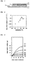
- FIG. 2 The relationship between the temperature of the substrate during film formation and the field effect mobility of a Cu-Pc film is illustrated in FIG. 2.
- FIG. 2 demonstrates that the field effect mobility of the Cu-Pc film increases dramatically as the temperature of the substrate increases from about 30°C to about 140°C. At substrate temperatures above 140°C, the trend reverses and the field effect mobility decreases with increasing temperature.
- the substituted phthalocyanines of the present invention are n-type semiconductors (i.e. the materials transport electrons).
- the materials are also stable in air.
- stable in air means that the electron transport properties of the semiconductor material do not degrade substantially over time in an air-containing atmosphere.
- Devices were formed using the above identified phthalocyanine coordination compounds as the active layer.
- a layer of each of the above-described phthalocyanine coordination compounds 21 was applied onto a separate n-doped silicon substrate to form the device 20 depicted in FIG. 2 and described generally above.
- the term substrate is used to refer to the structure of a silicon substrate 11 on which is formed a layer of gate dielectric 13 with two contacts 17 and 19 formed thereon.
- a third contact 15 is formed directly on the silicon substrate.
- the dielectric layer was 300 nm thick and had a capacitance (C i ) per unit area of 10 nF/cm 2 .
- the contacts were gold contacts.
- Devices were made having channel length of 25 ⁇ m, 12 ⁇ m, 4 ⁇ m, and 1.5 ⁇ m.
- the temperature of the substrate was controlled during the deposition of each film thereon to determine the effect of substrate temperature on the mobility and conductivity of the phthalocyanine layer.
- Individual films of each of the above-identified substituted phthalocyanines coordination compounds were formed on substrates heated to temperatures of 30°C, 125°C, and 215°C. Each film was formed using vacuum deposition in an evaporation chamber at a pressure of 2 x 10 -6 torr. About 50 mg of the phthalocyanine was placed in a tungsten boat. The boat was placed in a conventional evaporator system. The substrate was also placed in the evaporator on a copper block. A temperature controller was used to control the temperature of the copper block which, in turn, was used to control the temperature of the substrate. The boat was heated to a temperature of about 380°C and the phthalocyanine film was formed at a rate of about 0.4 nm to about 0.5 nm per second.
- the mobility of the devices clearly increased when the deposition temperature increased from 30°C to 125°C. Decreases in mobilities for some devices were observed when the deposition temperature was increased above about 150°C, however.
- the substituted phthalocyanine films formed at elevated temperature have an advantageous morphology for electron transport.
- the relationship between substrate temperature and the mobility of the resulting device depends somewhat on the metal coordinate in the substituted phthalocyanine coordination compound. For example, an advantageous mobility was observed throughout the entire temperature range of about 30°C to about 215°C when the metal coordinate was copper. However, an advantageous mobility was observed through the temperature range of about 100°C to about 215°C when the metal coordinate was iron. An advantageous mobility was observed through the temperature range of about 125°C to about 215°C when the metal coordinate was zinc.
- the measured mobilities of the fluorinated phthalocyanines were the highest.
- the halogen-substituted phthalocyanines were observed to be stable in air.
- the electron mobility and the on/off ratio of devices with halogen-substituted phthalocyanine semiconductors did not change substantially even after the devices were stored in open air for more than six months.
- the devices formed with the chlorine-substituted phthalocyanine material at 30°C did not demonstrate measurable field-effect mobility and the chlorine-substituted material desorbed (i.e., the films did not form) at 215°C. Therefore, it appears that the fluorine-substituted phthalocyanine materials can be deposited under a wider range of conditions than the chlorine-substituted phthalocyanine materials.
- FIG. 3 is a current-voltage curve obtained for a device with a F 16 CuPc semiconductor deposited on the substrate at a temperature of 125°C.
- the drain-source current ( ⁇ A) is reported as a function of the drain-source voltage (V) at various gate voltages.
- the measured device had a channel length of 12 ⁇ m.
- the film as deposited performs as an n-channel transistor.
Landscapes
- Chemical & Material Sciences (AREA)
- Inorganic Chemistry (AREA)
- Engineering & Computer Science (AREA)
- Materials Engineering (AREA)
- Physics & Mathematics (AREA)
- Optics & Photonics (AREA)
- Electromagnetism (AREA)
- Thin Film Transistor (AREA)
- Nitrogen Condensed Heterocyclic Rings (AREA)
- Photovoltaic Devices (AREA)
- Led Devices (AREA)
- Electroluminescent Light Sources (AREA)
Applications Claiming Priority (2)
| Application Number | Priority Date | Filing Date | Title |
|---|---|---|---|
| US97664997A | 1997-11-24 | 1997-11-24 | |
| US976649 | 1997-11-24 |
Publications (2)
| Publication Number | Publication Date |
|---|---|
| EP0921579A2 true EP0921579A2 (de) | 1999-06-09 |
| EP0921579A3 EP0921579A3 (de) | 1999-12-15 |
Family
ID=25524327
Family Applications (1)
| Application Number | Title | Priority Date | Filing Date |
|---|---|---|---|
| EP98309580A Withdrawn EP0921579A3 (de) | 1997-11-24 | 1998-11-24 | Dünfilmtransistor basierend auf substituierten Phthalocyaninen |
Country Status (4)
| Country | Link |
|---|---|
| EP (1) | EP0921579A3 (de) |
| JP (1) | JPH11251601A (de) |
| KR (1) | KR100336283B1 (de) |
| TW (1) | TW399338B (de) |
Cited By (12)
| Publication number | Priority date | Publication date | Assignee | Title |
|---|---|---|---|---|
| US6747287B1 (en) | 2001-10-18 | 2004-06-08 | Nec Corporation | Organic thin film transistor |
| WO2004087836A1 (en) * | 2003-03-31 | 2004-10-14 | Canon Kabushiki Kaisha | Field effect transistor and method of producing the same |
| EP1443570A3 (de) * | 2003-01-30 | 2005-11-09 | Changchun Institute of applied Chemistry Chinese Academy of Science | Organischer Dünnfilmtransistor mit einem Heteroübergang und einer Gatterisolationsschicht |
| WO2008003760A3 (en) * | 2006-07-06 | 2008-07-10 | Basf Se | THE USE OF CHLORINATED COPPER PHTHALOCYANINES AS AIR-STABLE n-CHANNEL ORGANIC SEMICONDUCTORS |
| EP1811573A4 (de) * | 2004-11-11 | 2010-03-24 | Mitsubishi Chem Corp | Feldeffekttransistor |
| US8022401B2 (en) | 2006-11-14 | 2011-09-20 | Idemitsu Kosan, Co., Ltd. | Organic thin film transistor and organic thin film light-emitting transistor |
| US8129494B2 (en) | 2006-12-26 | 2012-03-06 | Asahi Kasei E-Materials Corporation | Resin composition for printing plate |
| US8148720B2 (en) | 2006-11-24 | 2012-04-03 | Idemitsu Kosan Co., Ltd. | Organic thin film transistor and organic thin film light-emitting transistor |
| US8203139B2 (en) | 2006-11-24 | 2012-06-19 | Idemitsu Kosan Co., Ltd | Organic thin film transistor and organic thin film light-emitting transistor using an organic semiconductor layer having an aromatic hydrocarbon group or an aromatic heterocyclic group in the center thereof |
| US8207525B2 (en) | 2006-12-04 | 2012-06-26 | Idemitsu Kosan Co., Ltd. | Organic thin film transistor and organic thin film light emitting transistor |
| US8217389B2 (en) | 2006-10-12 | 2012-07-10 | Idemitsu Kosan, Co., Ltd. | Organic thin film transistor device and organic thin film light-emitting transistor |
| US8330147B2 (en) | 2006-12-04 | 2012-12-11 | Idemitsu Kosan, Co., Ltd. | Organic thin film transistor and organic thin film light emitting transistor having organic semiconductor compound with divalent aromatic hydrocarbon group and divalent aromatic heterocyclic group |
Families Citing this family (9)
| Publication number | Priority date | Publication date | Assignee | Title |
|---|---|---|---|---|
| US7193237B2 (en) | 2002-03-27 | 2007-03-20 | Mitsubishi Chemical Corporation | Organic semiconductor material and organic electronic device |
| WO2004075279A1 (ja) | 2003-02-18 | 2004-09-02 | Konica Minolta Holdings, Inc. | 有機薄膜トランジスタ素子及びその製造方法 |
| KR100965178B1 (ko) * | 2003-07-22 | 2010-06-24 | 삼성전자주식회사 | 유기반도체 패턴의 형성 방법과 이를 이용한 유기 박막트랜지스터의 제조 방법 |
| CA2540369A1 (en) | 2003-10-02 | 2005-04-07 | Nicolas Drolet | 2,7-carbazolenevinylene derivatives as novel materials in producing organic based electronic devices |
| JP4736318B2 (ja) * | 2003-11-28 | 2011-07-27 | Tdk株式会社 | 積層体の製造方法及び有機電界効果トランジスタの製造方法 |
| US7521710B2 (en) | 2006-02-16 | 2009-04-21 | Idemitsu Kosan Co., Ltd. | Organic thin film transistor |
| JP5405719B2 (ja) * | 2006-03-20 | 2014-02-05 | 富士フイルム株式会社 | フタロシアニン化合物、並びにそれを用いた半導体及び電子素子 |
| JPWO2008059817A1 (ja) | 2006-11-14 | 2010-03-04 | 出光興産株式会社 | 有機薄膜トランジスタ及び有機薄膜発光トランジスタ |
| CN101842917B (zh) * | 2007-10-31 | 2012-10-03 | 巴斯夫欧洲公司 | 卤化酞菁的用途 |
Family Cites Families (3)
| Publication number | Priority date | Publication date | Assignee | Title |
|---|---|---|---|---|
| NL233195A (de) * | 1957-11-13 | |||
| CA1030959A (en) * | 1973-11-27 | 1978-05-09 | Jost Von Der Crone | Halogen-containing metal phthalocyanines and a process for their manufacture |
| JPH08199161A (ja) * | 1995-01-26 | 1996-08-06 | Mitsubishi Chem Corp | 有機電界発光素子 |
-
1998
- 1998-10-28 TW TW087117899A patent/TW399338B/zh not_active IP Right Cessation
- 1998-11-23 KR KR19980050224A patent/KR100336283B1/ko not_active Expired - Fee Related
- 1998-11-24 EP EP98309580A patent/EP0921579A3/de not_active Withdrawn
- 1998-11-24 JP JP33315298A patent/JPH11251601A/ja active Pending
Cited By (16)
| Publication number | Priority date | Publication date | Assignee | Title |
|---|---|---|---|---|
| US6747287B1 (en) | 2001-10-18 | 2004-06-08 | Nec Corporation | Organic thin film transistor |
| EP1443570A3 (de) * | 2003-01-30 | 2005-11-09 | Changchun Institute of applied Chemistry Chinese Academy of Science | Organischer Dünnfilmtransistor mit einem Heteroübergang und einer Gatterisolationsschicht |
| WO2004087836A1 (en) * | 2003-03-31 | 2004-10-14 | Canon Kabushiki Kaisha | Field effect transistor and method of producing the same |
| US7094625B2 (en) | 2003-03-31 | 2006-08-22 | Canon Kabushiki Kaisha | Field effect transistor and method of producing the same |
| US8178397B2 (en) | 2004-11-11 | 2012-05-15 | Mitsubishi Chemical Corporation | Field effect transistor |
| EP1811573A4 (de) * | 2004-11-11 | 2010-03-24 | Mitsubishi Chem Corp | Feldeffekttransistor |
| WO2008003760A3 (en) * | 2006-07-06 | 2008-07-10 | Basf Se | THE USE OF CHLORINATED COPPER PHTHALOCYANINES AS AIR-STABLE n-CHANNEL ORGANIC SEMICONDUCTORS |
| US8217389B2 (en) | 2006-10-12 | 2012-07-10 | Idemitsu Kosan, Co., Ltd. | Organic thin film transistor device and organic thin film light-emitting transistor |
| US8022401B2 (en) | 2006-11-14 | 2011-09-20 | Idemitsu Kosan, Co., Ltd. | Organic thin film transistor and organic thin film light-emitting transistor |
| US8148720B2 (en) | 2006-11-24 | 2012-04-03 | Idemitsu Kosan Co., Ltd. | Organic thin film transistor and organic thin film light-emitting transistor |
| US8203139B2 (en) | 2006-11-24 | 2012-06-19 | Idemitsu Kosan Co., Ltd | Organic thin film transistor and organic thin film light-emitting transistor using an organic semiconductor layer having an aromatic hydrocarbon group or an aromatic heterocyclic group in the center thereof |
| US8207525B2 (en) | 2006-12-04 | 2012-06-26 | Idemitsu Kosan Co., Ltd. | Organic thin film transistor and organic thin film light emitting transistor |
| US8330147B2 (en) | 2006-12-04 | 2012-12-11 | Idemitsu Kosan, Co., Ltd. | Organic thin film transistor and organic thin film light emitting transistor having organic semiconductor compound with divalent aromatic hydrocarbon group and divalent aromatic heterocyclic group |
| TWI425688B (zh) * | 2006-12-04 | 2014-02-01 | Idemitsu Kosan Co | Organic thin film transistor and organic thin film emitting transistor |
| US8129494B2 (en) | 2006-12-26 | 2012-03-06 | Asahi Kasei E-Materials Corporation | Resin composition for printing plate |
| US8263730B2 (en) | 2006-12-26 | 2012-09-11 | Asahi Kasei E-Materials Corporation | Resin composition for printing plate |
Also Published As
| Publication number | Publication date |
|---|---|
| EP0921579A3 (de) | 1999-12-15 |
| KR19990045501A (ko) | 1999-06-25 |
| TW399338B (en) | 2000-07-21 |
| KR100336283B1 (ko) | 2002-09-18 |
| JPH11251601A (ja) | 1999-09-17 |
Similar Documents
| Publication | Publication Date | Title |
|---|---|---|
| US5969376A (en) | Organic thin film transistor having a phthalocyanine semiconductor layer | |
| EP0921579A2 (de) | Dünfilmtransistor basierend auf substituierten Phthalocyaninen | |
| Bao et al. | Organic field‐effect transistors with high mobility based on copper phthalocyanine | |
| Peng et al. | All‐organic thin‐film transistors made of alpha‐sexithienyl semiconducting and various polymeric insulating layers | |
| Gundlach et al. | Pentacene TFT with improved linear region characteristics using chemically modified source and drain electrodes | |
| Haddon et al. | C60 thin film transistors | |
| US8735882B2 (en) | ZnO based semiconductor devices and methods of manufacturing the same | |
| US8314425B2 (en) | Field-effect transistor using amorphouse oxide | |
| EP0716459A2 (de) | Artikel mit organischen Dünnfilmtransistoren | |
| US20050032268A1 (en) | Organic thin film transistor and method of manufacturing the same | |
| US9564481B2 (en) | Fully-printed carbon nanotube thin film transistor circuits for organic light emitting diode | |
| GB1572181A (en) | Device comprising a thin film of organic materila | |
| US20070056063A1 (en) | Process for modifying at least one electrical property of a nanotube or a nanowire and a transistor incorporating it | |
| US9755024B2 (en) | Functionalized ZnO or ZnO alloy films exhibiting high electron mobility | |
| US20060088875A1 (en) | Means for electrical contacting or isolation of organic or inorganic semiconductors and a method for its fabrication | |
| Roberts et al. | Photovoltaic properties of cadmium-telluride/Langmuir-film solar cells | |
| WO2006108272A2 (en) | Metal/fullerene anode structure and application of same | |
| Daraktchiev et al. | Ultrathin organic transistors on oxide surfaces | |
| US6429040B1 (en) | Device comprising a bipolar semi-conducting film | |
| US20060231954A1 (en) | Electric contact materials comprising organic heterojunction and device | |
| Kobayashi et al. | C60 thin-film transistors with high field-effect mobility, fabricated by molecular beam deposition | |
| Bouvet et al. | Electrical transduction in phthalocyanine-based gas sensors: from classical chemiresistors to new functional structures | |
| Clarisse et al. | The operation and characteristics of diphthalocyanine field effect transistors | |
| JP4429584B2 (ja) | 縦型の電界効果トランジスタ | |
| EP2506292A1 (de) | Verfahren zur herstellung einer kontaktstruktur für eine organische halbleitervorrichtung sowie kontaktstruktur für eine organische halbleitervorrichtung |
Legal Events
| Date | Code | Title | Description |
|---|---|---|---|
| PUAI | Public reference made under article 153(3) epc to a published international application that has entered the european phase |
Free format text: ORIGINAL CODE: 0009012 |
|
| AK | Designated contracting states |
Kind code of ref document: A2 Designated state(s): DE FR GB |
|
| AX | Request for extension of the european patent |
Free format text: AL;LT;LV;MK;RO;SI |
|
| PUAL | Search report despatched |
Free format text: ORIGINAL CODE: 0009013 |
|
| AK | Designated contracting states |
Kind code of ref document: A3 Designated state(s): AT BE CH CY DE DK ES FI FR GB GR IE IT LI LU MC NL PT SE |
|
| AX | Request for extension of the european patent |
Free format text: AL;LT;LV;MK;RO;SI |
|
| 17P | Request for examination filed |
Effective date: 20000602 |
|
| AKX | Designation fees paid |
Free format text: DE FR GB |
|
| STAA | Information on the status of an ep patent application or granted ep patent |
Free format text: STATUS: THE APPLICATION HAS BEEN WITHDRAWN |
|
| 18W | Application withdrawn |
Effective date: 20030522 |