EP0921613A2 - Laser compact à matériaux solides et transmetteur utilisant le même - Google Patents
Laser compact à matériaux solides et transmetteur utilisant le même Download PDFInfo
- Publication number
- EP0921613A2 EP0921613A2 EP98122689A EP98122689A EP0921613A2 EP 0921613 A2 EP0921613 A2 EP 0921613A2 EP 98122689 A EP98122689 A EP 98122689A EP 98122689 A EP98122689 A EP 98122689A EP 0921613 A2 EP0921613 A2 EP 0921613A2
- Authority
- EP
- European Patent Office
- Prior art keywords
- laser
- gain crystal
- mirror
- chirped mirror
- cavity
- Prior art date
- Legal status (The legal status is an assumption and is not a legal conclusion. Google has not performed a legal analysis and makes no representation as to the accuracy of the status listed.)
- Granted
Links
- 239000013078 crystal Substances 0.000 claims abstract description 58
- 238000005086 pumping Methods 0.000 claims abstract description 32
- 239000006185 dispersion Substances 0.000 claims abstract description 8
- 230000003287 optical effect Effects 0.000 claims description 47
- 239000011248 coating agent Substances 0.000 claims description 18
- 238000000576 coating method Methods 0.000 claims description 18
- 238000004891 communication Methods 0.000 claims description 12
- 239000004065 semiconductor Substances 0.000 claims description 9
- 239000006096 absorbing agent Substances 0.000 claims description 7
- 239000011521 glass Substances 0.000 claims description 4
- 201000009310 astigmatism Diseases 0.000 claims description 3
- PNEYBMLMFCGWSK-UHFFFAOYSA-N aluminium oxide Inorganic materials [O-2].[O-2].[O-2].[Al+3].[Al+3] PNEYBMLMFCGWSK-UHFFFAOYSA-N 0.000 claims description 2
- 229910052593 corundum Inorganic materials 0.000 claims description 2
- 229910052839 forsterite Inorganic materials 0.000 claims description 2
- 239000007787 solid Substances 0.000 claims description 2
- 229910001845 yogo sapphire Inorganic materials 0.000 claims description 2
- 239000000758 substrate Substances 0.000 claims 2
- 230000008030 elimination Effects 0.000 abstract 1
- 238000003379 elimination reaction Methods 0.000 abstract 1
- 238000010586 diagram Methods 0.000 description 11
- 238000001228 spectrum Methods 0.000 description 4
- VYPSYNLAJGMNEJ-UHFFFAOYSA-N Silicium dioxide Chemical compound O=[Si]=O VYPSYNLAJGMNEJ-UHFFFAOYSA-N 0.000 description 2
- 239000005350 fused silica glass Substances 0.000 description 2
- 230000010355 oscillation Effects 0.000 description 2
- 229910017502 Nd:YVO4 Inorganic materials 0.000 description 1
- 238000010521 absorption reaction Methods 0.000 description 1
- 230000005540 biological transmission Effects 0.000 description 1
- 238000005516 engineering process Methods 0.000 description 1
- 239000000463 material Substances 0.000 description 1
- 238000005259 measurement Methods 0.000 description 1
- 239000013307 optical fiber Substances 0.000 description 1
- 230000010287 polarization Effects 0.000 description 1
- 230000010349 pulsation Effects 0.000 description 1
- 238000000926 separation method Methods 0.000 description 1
- 238000004611 spectroscopical analysis Methods 0.000 description 1
Images



Classifications
-
- H—ELECTRICITY
- H04—ELECTRIC COMMUNICATION TECHNIQUE
- H04B—TRANSMISSION
- H04B10/00—Transmission systems employing electromagnetic waves other than radio-waves, e.g. infrared, visible or ultraviolet light, or employing corpuscular radiation, e.g. quantum communication
- H04B10/50—Transmitters
-
- H—ELECTRICITY
- H01—ELECTRIC ELEMENTS
- H01S—DEVICES USING THE PROCESS OF LIGHT AMPLIFICATION BY STIMULATED EMISSION OF RADIATION [LASER] TO AMPLIFY OR GENERATE LIGHT; DEVICES USING STIMULATED EMISSION OF ELECTROMAGNETIC RADIATION IN WAVE RANGES OTHER THAN OPTICAL
- H01S3/00—Lasers, i.e. devices using stimulated emission of electromagnetic radiation in the infrared, visible or ultraviolet wave range
- H01S3/05—Construction or shape of optical resonators; Accommodation of active medium therein; Shape of active medium
- H01S3/08—Construction or shape of optical resonators or components thereof
- H01S3/08059—Constructional details of the reflector, e.g. shape
-
- H—ELECTRICITY
- H01—ELECTRIC ELEMENTS
- H01S—DEVICES USING THE PROCESS OF LIGHT AMPLIFICATION BY STIMULATED EMISSION OF RADIATION [LASER] TO AMPLIFY OR GENERATE LIGHT; DEVICES USING STIMULATED EMISSION OF ELECTROMAGNETIC RADIATION IN WAVE RANGES OTHER THAN OPTICAL
- H01S3/00—Lasers, i.e. devices using stimulated emission of electromagnetic radiation in the infrared, visible or ultraviolet wave range
- H01S3/02—Constructional details
- H01S3/025—Constructional details of solid state lasers, e.g. housings or mountings
-
- H—ELECTRICITY
- H01—ELECTRIC ELEMENTS
- H01S—DEVICES USING THE PROCESS OF LIGHT AMPLIFICATION BY STIMULATED EMISSION OF RADIATION [LASER] TO AMPLIFY OR GENERATE LIGHT; DEVICES USING STIMULATED EMISSION OF ELECTROMAGNETIC RADIATION IN WAVE RANGES OTHER THAN OPTICAL
- H01S3/00—Lasers, i.e. devices using stimulated emission of electromagnetic radiation in the infrared, visible or ultraviolet wave range
- H01S3/05—Construction or shape of optical resonators; Accommodation of active medium therein; Shape of active medium
- H01S3/06—Construction or shape of active medium
- H01S3/0602—Crystal lasers or glass lasers
- H01S3/0606—Crystal lasers or glass lasers with polygonal cross-section, e.g. slab, prism
-
- H—ELECTRICITY
- H01—ELECTRIC ELEMENTS
- H01S—DEVICES USING THE PROCESS OF LIGHT AMPLIFICATION BY STIMULATED EMISSION OF RADIATION [LASER] TO AMPLIFY OR GENERATE LIGHT; DEVICES USING STIMULATED EMISSION OF ELECTROMAGNETIC RADIATION IN WAVE RANGES OTHER THAN OPTICAL
- H01S3/00—Lasers, i.e. devices using stimulated emission of electromagnetic radiation in the infrared, visible or ultraviolet wave range
- H01S3/05—Construction or shape of optical resonators; Accommodation of active medium therein; Shape of active medium
- H01S3/06—Construction or shape of active medium
- H01S3/0619—Coatings, e.g. AR, HR, passivation layer
- H01S3/0621—Coatings on the end-faces, e.g. input/output surfaces of the laser light
-
- H—ELECTRICITY
- H01—ELECTRIC ELEMENTS
- H01S—DEVICES USING THE PROCESS OF LIGHT AMPLIFICATION BY STIMULATED EMISSION OF RADIATION [LASER] TO AMPLIFY OR GENERATE LIGHT; DEVICES USING STIMULATED EMISSION OF ELECTROMAGNETIC RADIATION IN WAVE RANGES OTHER THAN OPTICAL
- H01S3/00—Lasers, i.e. devices using stimulated emission of electromagnetic radiation in the infrared, visible or ultraviolet wave range
- H01S3/10—Controlling the intensity, frequency, phase, polarisation or direction of the emitted radiation, e.g. switching, gating, modulating or demodulating
- H01S3/11—Mode locking; Q-switching; Other giant-pulse techniques, e.g. cavity dumping
- H01S3/1106—Mode locking
- H01S3/1112—Passive mode locking
Definitions
- the present invention relates to a compact solid-state laser, and particularly to a compact solid-state laser used for the multiwavelength optical source for the wavelength-division-multiplexed communication system, the wide-spectrum optical source for spectroscopy, the ultra-short pulse source for distance measurement, the ultra-short pulse source for instrumentation, and the like.
- the invention also relates to a transmitter using this compact solid-state laser.
- this basic structure has too many component parts and needs to space out the prism pair or grating pair by several tens centimeters for dispersion compensation, and therefore it does not allow the compact design of solid-state laser.
- the repetition frequency cannot be raised unless the cavity length is made short.
- the conventional solid-state laser has a repetition frequency of around 100 MHz, whereas the solid-state laser used for the communication system must have a repetition frequency of several gigahertz or higher.
- the present invention is intended to offer a compact solid-state laser which is designed to compensate the dispersion by means of a chirped mirror formed by multilayer coating (described in the article entitled “Chirped multilayer coating for broadband dispersion control in femtsecond laser” by Robert Szipocs et al. in OPTICS LETTERS, Vol.19, No.3, pp.201-203, published in 1994), so that the cavity is virtually formed of only two elements of a chirped mirror and a gain crystal.
- the gain crystal has its one side rendered the reflection coating, chirped-mirror coating, or saturable-absorber mirror coating so that it functions as a mirror, with the chirped mirror serving for another mirror of the cavity, thereby reducing the number of mirrors required.
- Fig. 1 through Fig. 4 show the arrangements of compact solid-state laser based on the embodiments of this invention.
- the compact solid-state laser has its cavity formed between the right-side reflection surface 1a of a gain crystal 1 and the right-side reflection surface 2a of a chirped mirror 2.
- Reference numeral 6 denotes the pumping light directed to the gain crystal 1
- 3 is the optical source of the pumping light
- 4 is the laser output
- 5 is a dichroic mirror which diverts the course of the laser output 4.
- the compact solid-state laser can have several arrangements depending on the manner of leading in the pumping light 6 and leading out the laser output 4, of which four representative types are shown in Fig. 1 through Fig. 4.
- the pumping light 6 is incident to the chirped mirror 2 from its back, and the laser output 4 is led out from the reflection surface 1a of the gain crystal 1.
- the pumping light 6 is incident to the reflection surface 1a of the gain crystal 1, and the laser output 4 is led out from the back of the chirped mirror 2.
- the pumping light 6 is introduced into the cavity by being incident to the back of the chirped mirror 2 through the dichroic mirror 5, and the laser output 4 is taken out from the back of the chirped mirror 2 and led out by being diverted by the dichroic mirror 5.
- the pumping light 6 and the laser output 4 exist on the side of the right-side reflection surface 1a.
- the pumping light 6 is introduced into the cavity by being incident to the reflection surface 1a of the gain crystal 1 through the dichroic mirror 5, and the laser output 4 is taken out from the reflection surface 1a of the gain crystal 1 and led out by being diverted by the dichroic mirror 5.
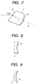
- the gain crystal 1 used in the foregoing arrangements of solid-state laser can have various structures as shown in Fig. 5, Fig. 6 and Fig. 7.
- the gain crystal 1 has its right-side reflection surface 1a rendered the reflection coating, chirped mirror coating, or saturable-absorber mirror coating.
- the reflection surface 1a is coated to become an output-coupler mirror of several percent or less.
- the gain crystal 1 has its reflection surface 1a rendered the high-reflection coating.
- the gain crystal 1 has its left-side surface 1b rendered the anti-reflection coating, and further may be rendered the saturable-absorber coating, instead of the saturable-absorber mirror coating of the reflection surface 1a, as shown in Fig. 5. Or, the gain crystal 1 is polished to provide a Brewster angle ⁇ B so as to suppress the reflection, as shown in Fig. 6 and Fig. 7. Shown in Fig. 6 is the simplest structure of gain crystal having a Brewster angle ⁇ B , with its reflection surface 1a being rendered the planar cutting.
- the Brewster angle ⁇ B differs slightly depending on the wavelength. Accordingly, in dealing with a wide spectrum as in the case of ultra-short pulse oscillator, the optical path varies in the gain crystal 1. It can be correct effectively by the provision of a cylindrical curving surface for the reflection surface 1a as shown in Fig. 7. Shown by the dashed line 6 in Fig. 6 and Fig. 7 is the incident pumping light 6 of the case of incidence on the side of the reflection surface 1a.
- Fig. 8 and Fig. 9 show examples of the structure of chirped mirror 2 which can be used in the foregoing arrangements of solid-state laser.
- the chirped mirror 2 is a concave mirror having a focal distance of around several tens millimeters, which is determined depending on the repetition frequency.
- the chirped mirror has a multilayer coating on the right-side surface 2a as shown in Fig. 8 and Fig. 9.
- the chirped mirror 2 may have its unused back surface (opposite to its mirror surface 2a) simply left planar as shown in Fig. 8.
- the respective optical systems are required on that side.
- the mirror 2 may have its back surface simply left planar as shown in Fig. 8.
- the chirped mirror 2 may be designed to have its solid body working as a focusing lens so that the whole device becomes much smaller.
- the pumping optical source 3 is a solid-state laser or a semiconductor laser, the latter being useful for the compactness of the whole device.
- the pumping optical source 3 may include a lens system for the enhancement of pumping ability, and may include an isolator, also.
- the pumping optical source 3, gain crystal 1 and chirped mirror 2 have a common optical axis obviously, as will be explained in regard to the structure in connection with the transmitter of optical communication system.
- gain crystal 1 is a Brewster-cut one like Fig. 6 or Fig. 7, and that pumping light 6 is introduced into the cavity through the chirped mirror 2 like Fig. 1 or Fig. 3, then the lens 32 in optical source 30 is tilted by a few or more degrees to compensate astigmatism, as shown in Fig. 10, where an isolator 33 is also drawn.
- a glass or fused-silica plate 34 may be set in the cavity at a Brewster angle q B , as shown in Fig. 11.
- the compact solid-state laser used in this transmitter adopts the Cr:YAG crystal having an oscillation wavelength of the 1.5- ⁇ m band.
- the absorption band of the Cr:YAG crystal has a peak at a wavelength around 1.05 ⁇ m.
- a solid-state laser of Nd:YVO 4 , Nd:YLF or Nd:YAG, or a semiconductor laser can be used.
- the Cr:YAG laser has a wide spectrum (200 nm at maximum) when it is operated in ultra-short pulse oscillation, and accordingly it is useful for the optical source of the wavelength-division-multiplexed communication system.
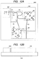
- Figs. 12A and 12B show the plan view and side view of a transmitter of wavelength-division-multiplexed communication system which employs a compact solid-state laser of Cr:YAG.
- Indicated by 4000 is the Cr:YAG laser, which consists of a pumping optical source 3, a gain crystal 1 and a chirped mirror 2, as has been shown in Fig. 2, and it provides all wavelengths necessary for the wavelength-division-multiplexed communication system.
- Indicated by 1000 is a signal synthesizer, which converts the light, which comes from the Cr:YAG laser 4000 and is incident to the optical fiber 101, into wavelength-division-multiplexed signals in response to the signals to be transmitted.
- Indicated by 3000 is a constant-temperature maintaining device, which maintains the suitable temperature for the operation of the signal synthesizer 1000 and Cr:YAG laser 4000 and also serves for the chassis of these parts.
- the signal synthesizer 1000 can be the one that has been offered in the U.S. Patent Application Serial No.08/997,700 (and the corresponding EP patent publication EP 0 851 205) which is the preceding patent application of the present application, and it will be explained here only briefly.
- the incident light from Cr:YAG laser 4000 is introduced into a waveguide 101.
- the incident light is introduced into an optical path constituting the interferometer 100 through the waveguide 101. Since the other waveguide 102 contacts the waveguide 101 so as to form a separation path in the interferometer 100, the incident light is divided into two optical-paths corresponding to the waveguides 101 and 102. These two optical-paths are brought into contact with each other again at positions where their optical path lengths differ from each other. As a result, interference occurs in the above-described incident light and hence waveforms having predetermined spectrum are obtained from exits of the optical paths 101 and 102.
- the light emitted from the optical path 101 and the light emitted from the optical path 102 are introduced into the multichannel modulators 200 and 300, respectively.
- the multichannel modulators 200 and 300 are substantially identical in configuration to each other.
- the light or optical pulses launched from the optical paths 101 and 102 to the multichannel modulators 200 and 300 are set to parallel light beams by cut-away portions 201 and 301 having plano-concave shapes acting plano-convex lenses, respectively.
- the parallel light beams transmitted through the cut-away portions 201 and 301 are respectively introduced to cut-away portions 211 and 311 serving as diffraction gratings.
- the light or optical pulses separated into every frequency by the diffraction gratings 211 and 311 are focused on the spatial light modulators 231 and 331 every frequency through cut-away portions 221 an 321 acting plano-convex lenses.
- the spatial light modulators 231 and 331 allow the light or optical pulses subjected to optical modulation every frequency to pass therethrough according to the modulating signals S 1 and S 2 because voltages for varying absorptance or refractive index are respectively applied to focusing positions associated with each frequency.
- the optical pulses transmitted through the spatial light modulators 231 and 331 are respectively introduced to cut-away portions 251 and 351 used to serve as diffraction gratings through cut-away portions 241 and 341 functioning as plano-convex lenses, where they are restored to the parallel light beams.
- the optical pulses restored to the parallel light beams are focused on their corresponding optical paths 103 and 104 through cut-away portions 261 and 361 acting plano-convex lenses.
- the optical pulses introduced into the optical paths 103 and 104 are coupled by the optical coupler 400 so that a signal waveform for sending is obtained.
- signal lines for the spatial light modulators 231 and 331 are omitted.
- the output signal is transmitted in an arbitrary manner to a receiving terminal, in which the signal is demultiplexed by means of a proper demultiplexer and detected in terms of individual wavelengths by means of proper detectors.
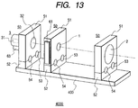
- Fig. 13 explains the compact solid-state laser 4000 shown in Fig. 12.
- part holders 50 each consisting of a holder 51 for mounting the pumping optical source 3, gain crystal 1 or chirped mirror 2, and a fixture 52 which serves to fix the holder 50 to the base plate 400.
- a pair of vertical angle adjusting means 53 and horizontal angle adjusting means 54 are equipped between the holder 51 and fixture 52. After the parts 3, 1 and 2 are mounted on the holders 51 and the fixtures 52 are fixed to the base plate 400, the angle adjusting means 53 and 54 are operated so that these parts have a common optical axis as shown by the dash-dot line.
- the part holders 50 and associated angle adjusting means 53 and 54 which are shown very simply in the figure, are specifically commercially-available holders named "CENTER MOUNT", Models 9807,9813M & 9855 manufactured by ⁇ -Focus (Corp.), or holders named "ULTIMA Series” manufactured by Newport (Corp.), for example.
- the pumping optical source 3 is made up of a semiconductor laser 31 and a convergent lens 32.
- the pumping optical source 3 may also include an isolator between the convergent lens 32 and the gain crystal 1 although it is not shown in Fig.13.
- the gain crystal 1 produces much heat which cannot be conducted sufficiently to the constant-temperature maintaining device 3000 through the part holder 50 and base plate 400, and therefore there are attached Peltier's elements 61 on both side walls of the holder 51 of the gain crystal 1.
- Another Peltier's element 63 is attached to the pumping optical source 3 in its section close to the semiconductor laser 31, so that the laser 31 is cooled and the tuning of wavelength based on temperature control is make possible.
- the wiring of the Peltier's elements are not shown in the figure.
- the transmitter can be made compact based on the compact solid-state laser and signal synthesizer.
- the conventional solid-state laser is not small enough, and therefore it is virtually limited to experimental uses by specialists.
- the inventive compact solid-state laser is capable of being built in a variety of measuring instruments.
- multiple laser devices are arrayed to arrange optical sources, whereas, using such a solid-state laser as a Cr:YAG laser enables the generation of multiple wavelengths from a single optical source.
- the inventive compact solid-state laser which is operative at a higher repetition frequency can readily be incorporated in the wavelength-division-multiplexed communication equipment, and it will increase significantly the transmission capacity of wavelength-division-multiplexed communication system.
Landscapes
- Physics & Mathematics (AREA)
- Electromagnetism (AREA)
- Engineering & Computer Science (AREA)
- Computer Networks & Wireless Communication (AREA)
- Signal Processing (AREA)
- Plasma & Fusion (AREA)
- Optics & Photonics (AREA)
- Lasers (AREA)
Applications Claiming Priority (2)
| Application Number | Priority Date | Filing Date | Title |
|---|---|---|---|
| JP33527697 | 1997-12-05 | ||
| JP9335276A JPH11168252A (ja) | 1997-12-05 | 1997-12-05 | 小型固体レーザー |
Publications (3)
| Publication Number | Publication Date |
|---|---|
| EP0921613A2 true EP0921613A2 (fr) | 1999-06-09 |
| EP0921613A3 EP0921613A3 (fr) | 2000-08-23 |
| EP0921613B1 EP0921613B1 (fr) | 2003-02-19 |
Family
ID=18286717
Family Applications (1)
| Application Number | Title | Priority Date | Filing Date |
|---|---|---|---|
| EP98122689A Expired - Lifetime EP0921613B1 (fr) | 1997-12-05 | 1998-11-30 | Laser compact à matériau amplificateur solide et transmetteur utilisant le même matériau |
Country Status (3)
| Country | Link |
|---|---|
| EP (1) | EP0921613B1 (fr) |
| JP (1) | JPH11168252A (fr) |
| DE (1) | DE69811463T2 (fr) |
Cited By (2)
| Publication number | Priority date | Publication date | Assignee | Title |
|---|---|---|---|---|
| EP1143581A3 (fr) * | 2000-04-05 | 2004-09-15 | Hitachi, Ltd. | Laser à l'état solide et émetteur optique |
| EP2180562A1 (fr) * | 2008-10-23 | 2010-04-28 | Fujifilm Corporation | Laser à l'état solide compact à blocage de mode |
Families Citing this family (11)
| Publication number | Priority date | Publication date | Assignee | Title |
|---|---|---|---|---|
| KR100757101B1 (ko) | 2005-12-06 | 2007-09-10 | 광주과학기술원 | 고반복률 펨토초 재생 증폭 장치 |
| JP2008028379A (ja) * | 2006-06-22 | 2008-02-07 | Fujifilm Corp | モードロックレーザ装置 |
| EP1870972A1 (fr) | 2006-06-22 | 2007-12-26 | Fujifilm Corporation | Dispositif laser à mode couplé |
| JP2009016607A (ja) * | 2007-07-05 | 2009-01-22 | Fujifilm Corp | モードロックレーザ装置 |
| US7864821B2 (en) | 2007-09-28 | 2011-01-04 | Fujifilm Corporation | Mode-locked solid-state laser apparatus |
| EP2042893A3 (fr) | 2007-09-28 | 2010-12-15 | Fujinon Corporation | Miroir à dispersion négative et appareil laser à l'état solide à mode bloqué incluant le miroir |
| JP5456994B2 (ja) | 2008-06-20 | 2014-04-02 | 富士フイルム株式会社 | モード同期固体レーザ装置 |
| JP5456992B2 (ja) | 2008-06-20 | 2014-04-02 | 富士フイルム株式会社 | モード同期固体レーザ装置 |
| JP5456993B2 (ja) | 2008-06-20 | 2014-04-02 | 富士フイルム株式会社 | モード同期固体レーザ装置 |
| JP2010258198A (ja) | 2009-04-24 | 2010-11-11 | Fujifilm Corp | モード同期固体レーザ装置 |
| US8953651B2 (en) * | 2010-02-24 | 2015-02-10 | Alcon Lensx, Inc. | High power femtosecond laser with repetition rate adjustable according to scanning speed |
Family Cites Families (2)
| Publication number | Priority date | Publication date | Assignee | Title |
|---|---|---|---|---|
| JPH0425084A (ja) * | 1990-05-16 | 1992-01-28 | Mitsubishi Electric Corp | 固体レーザ装置 |
| EP0851205B1 (fr) * | 1996-12-26 | 2003-03-26 | Hitachi, Ltd. | Interféromètre optique et synthétiseur de signal utilisant l'interféromètre |
-
1997
- 1997-12-05 JP JP9335276A patent/JPH11168252A/ja active Pending
-
1998
- 1998-11-30 EP EP98122689A patent/EP0921613B1/fr not_active Expired - Lifetime
- 1998-11-30 DE DE69811463T patent/DE69811463T2/de not_active Expired - Fee Related
Cited By (3)
| Publication number | Priority date | Publication date | Assignee | Title |
|---|---|---|---|---|
| EP1143581A3 (fr) * | 2000-04-05 | 2004-09-15 | Hitachi, Ltd. | Laser à l'état solide et émetteur optique |
| EP2180562A1 (fr) * | 2008-10-23 | 2010-04-28 | Fujifilm Corporation | Laser à l'état solide compact à blocage de mode |
| JP2010103291A (ja) * | 2008-10-23 | 2010-05-06 | Fujifilm Corp | モード同期レーザ装置 |
Also Published As
| Publication number | Publication date |
|---|---|
| EP0921613B1 (fr) | 2003-02-19 |
| DE69811463T2 (de) | 2004-01-15 |
| JPH11168252A (ja) | 1999-06-22 |
| EP0921613A3 (fr) | 2000-08-23 |
| DE69811463D1 (de) | 2003-03-27 |
Similar Documents
| Publication | Publication Date | Title |
|---|---|---|
| US6229835B1 (en) | Compact solid-state laser and transmitter using the same | |
| US6226424B1 (en) | Integrated wavelength-select transmitter | |
| JP3726676B2 (ja) | 外部共振器型モード同期半導体レーザ装置 | |
| US6572278B2 (en) | Opto-electronic device having staked connection between parts to prevent differential thermal expansion | |
| EP0921613B1 (fr) | Laser compact à matériau amplificateur solide et transmetteur utilisant le même matériau | |
| US5825792A (en) | Wavelength monitoring and control assembly for WDM optical transmission systems | |
| US9246595B2 (en) | Small packaged tunable laser transmitter | |
| JP4449060B2 (ja) | 光ファイバにおける色分散の補償装置及び方法 | |
| CA2327654A1 (fr) | Interferometre non lineaire pour multiplexeur a division de longueur d'onde dense a fibre optique utilisant un procede de phase differentielle de separation de longueur d'onde | |
| US6795479B2 (en) | Generation of optical pulse train having high repetition rate using mode-locked laser | |
| US20030072336A1 (en) | Miniaturized internal laser stabilizing apparatus with inline output for fiber optic applications | |
| JP2010093078A (ja) | 光学素子、レーザ光発振装置及びレーザ光増幅装置 | |
| US6754248B2 (en) | Solid-state laser and optical transmitter | |
| JP2010020105A (ja) | 光半導体装置及びその製造方法 | |
| CA2329089A1 (fr) | Stabilisation a retroaction d'une diode laser a grande surface par un reseau de fibres | |
| JP2002252401A (ja) | レーザ装置 | |
| US20020075914A1 (en) | Semiconductor laser module, laser unit, and raman amplifier | |
| US20250167506A1 (en) | Laser amplifier utilizing multiple end pump spots and method of manufacture | |
| US20030035608A1 (en) | Multi-channel compensation of chromatic dispersion slope using etalons with wavelength dependent variable reflectivity | |
| JP6507659B2 (ja) | 光モジュールの製造方法 | |
| JPWO2001005003A1 (ja) | レーザ装置 | |
| US12308609B2 (en) | Integration of optical gain subassembly with silicon photonics | |
| US20040208543A1 (en) | Multiplexer and pulse generating laser device | |
| EP1037336A2 (fr) | Laser à l'ètat solid compensè pour l'astigmatism de la lumière de pompage | |
| US20050094696A1 (en) | Compact front facet tap for laser device |
Legal Events
| Date | Code | Title | Description |
|---|---|---|---|
| PUAI | Public reference made under article 153(3) epc to a published international application that has entered the european phase |
Free format text: ORIGINAL CODE: 0009012 |
|
| AK | Designated contracting states |
Kind code of ref document: A2 Designated state(s): DE FR GB IT SE |
|
| AX | Request for extension of the european patent |
Free format text: AL;LT;LV;MK;RO;SI |
|
| PUAL | Search report despatched |
Free format text: ORIGINAL CODE: 0009013 |
|
| AK | Designated contracting states |
Kind code of ref document: A3 Designated state(s): AT BE CH CY DE DK ES FI FR GB GR IE IT LI LU MC NL PT SE |
|
| AX | Request for extension of the european patent |
Free format text: AL;LT;LV;MK;RO;SI |
|
| 17P | Request for examination filed |
Effective date: 20000919 |
|
| AKX | Designation fees paid |
Free format text: DE FR GB IT SE |
|
| GRAG | Despatch of communication of intention to grant |
Free format text: ORIGINAL CODE: EPIDOS AGRA |
|
| 17Q | First examination report despatched |
Effective date: 20020213 |
|
| GRAG | Despatch of communication of intention to grant |
Free format text: ORIGINAL CODE: EPIDOS AGRA |
|
| GRAG | Despatch of communication of intention to grant |
Free format text: ORIGINAL CODE: EPIDOS AGRA |
|
| GRAH | Despatch of communication of intention to grant a patent |
Free format text: ORIGINAL CODE: EPIDOS IGRA |
|
| GRAH | Despatch of communication of intention to grant a patent |
Free format text: ORIGINAL CODE: EPIDOS IGRA |
|
| GRAA | (expected) grant |
Free format text: ORIGINAL CODE: 0009210 |
|
| AK | Designated contracting states |
Designated state(s): DE FR GB IT SE |
|
| REG | Reference to a national code |
Ref country code: GB Ref legal event code: FG4D |
|
| REF | Corresponds to: |
Ref document number: 69811463 Country of ref document: DE Date of ref document: 20030327 Kind code of ref document: P |
|
| REG | Reference to a national code |
Ref country code: SE Ref legal event code: TRGR |
|
| ET | Fr: translation filed | ||
| PG25 | Lapsed in a contracting state [announced via postgrant information from national office to epo] |
Ref country code: SE Free format text: LAPSE BECAUSE OF NON-PAYMENT OF DUE FEES Effective date: 20031201 |
|
| PLBE | No opposition filed within time limit |
Free format text: ORIGINAL CODE: 0009261 |
|
| STAA | Information on the status of an ep patent application or granted ep patent |
Free format text: STATUS: NO OPPOSITION FILED WITHIN TIME LIMIT |
|
| 26N | No opposition filed |
Effective date: 20031120 |
|
| EUG | Se: european patent has lapsed | ||
| PGFP | Annual fee paid to national office [announced via postgrant information from national office to epo] |
Ref country code: FR Payment date: 20051024 Year of fee payment: 8 |
|
| PGFP | Annual fee paid to national office [announced via postgrant information from national office to epo] |
Ref country code: GB Payment date: 20051109 Year of fee payment: 8 |
|
| PG25 | Lapsed in a contracting state [announced via postgrant information from national office to epo] |
Ref country code: IT Free format text: LAPSE BECAUSE OF NON-PAYMENT OF DUE FEES;WARNING: LAPSES OF ITALIAN PATENTS WITH EFFECTIVE DATE BEFORE 2007 MAY HAVE OCCURRED AT ANY TIME BEFORE 2007. THE CORRECT EFFECTIVE DATE MAY BE DIFFERENT FROM THE ONE RECORDED. Effective date: 20051130 |
|
| PGFP | Annual fee paid to national office [announced via postgrant information from national office to epo] |
Ref country code: DE Payment date: 20051202 Year of fee payment: 8 |
|
| PG25 | Lapsed in a contracting state [announced via postgrant information from national office to epo] |
Ref country code: DE Free format text: LAPSE BECAUSE OF NON-PAYMENT OF DUE FEES Effective date: 20070601 |
|
| GBPC | Gb: european patent ceased through non-payment of renewal fee |
Effective date: 20061130 |
|
| REG | Reference to a national code |
Ref country code: FR Ref legal event code: ST Effective date: 20070731 |
|
| PG25 | Lapsed in a contracting state [announced via postgrant information from national office to epo] |
Ref country code: GB Free format text: LAPSE BECAUSE OF NON-PAYMENT OF DUE FEES Effective date: 20061130 |
|
| PG25 | Lapsed in a contracting state [announced via postgrant information from national office to epo] |
Ref country code: FR Free format text: LAPSE BECAUSE OF NON-PAYMENT OF DUE FEES Effective date: 20061130 |