EP0923121A1 - Verfahren zur Herstellung von Dünnschichtvorrichtungen unter Verwendung der anisotropen Reflektionstechnik - Google Patents
Verfahren zur Herstellung von Dünnschichtvorrichtungen unter Verwendung der anisotropen Reflektionstechnik Download PDFInfo
- Publication number
- EP0923121A1 EP0923121A1 EP98402985A EP98402985A EP0923121A1 EP 0923121 A1 EP0923121 A1 EP 0923121A1 EP 98402985 A EP98402985 A EP 98402985A EP 98402985 A EP98402985 A EP 98402985A EP 0923121 A1 EP0923121 A1 EP 0923121A1
- Authority
- EP
- European Patent Office
- Prior art keywords
- layer
- etching
- signature
- silicon
- sample
- Prior art date
- Legal status (The legal status is an assumption and is not a legal conclusion. Google has not performed a legal analysis and makes no representation as to the accuracy of the status listed.)
- Withdrawn
Links
Images


Classifications
-
- H—ELECTRICITY
- H10—SEMICONDUCTOR DEVICES; ELECTRIC SOLID-STATE DEVICES NOT OTHERWISE PROVIDED FOR
- H10P—GENERIC PROCESSES OR APPARATUS FOR THE MANUFACTURE OR TREATMENT OF DEVICES COVERED BY CLASS H10
- H10P74/00—Testing or measuring during manufacture or treatment of wafers, substrates or devices
- H10P74/23—Testing or measuring during manufacture or treatment of wafers, substrates or devices characterised by multiple measurements, corrections, marking or sorting processes
- H10P74/238—Testing or measuring during manufacture or treatment of wafers, substrates or devices characterised by multiple measurements, corrections, marking or sorting processes comprising acting in response to an ongoing measurement without interruption of processing, e.g. endpoint detection or in-situ thickness measurement
-
- C—CHEMISTRY; METALLURGY
- C23—COATING METALLIC MATERIAL; COATING MATERIAL WITH METALLIC MATERIAL; CHEMICAL SURFACE TREATMENT; DIFFUSION TREATMENT OF METALLIC MATERIAL; COATING BY VACUUM EVAPORATION, BY SPUTTERING, BY ION IMPLANTATION OR BY CHEMICAL VAPOUR DEPOSITION, IN GENERAL; INHIBITING CORROSION OF METALLIC MATERIAL OR INCRUSTATION IN GENERAL
- C23C—COATING METALLIC MATERIAL; COATING MATERIAL WITH METALLIC MATERIAL; SURFACE TREATMENT OF METALLIC MATERIAL BY DIFFUSION INTO THE SURFACE, BY CHEMICAL CONVERSION OR SUBSTITUTION; COATING BY VACUUM EVAPORATION, BY SPUTTERING, BY ION IMPLANTATION OR BY CHEMICAL VAPOUR DEPOSITION, IN GENERAL
- C23C14/00—Coating by vacuum evaporation, by sputtering or by ion implantation of the coating forming material
- C23C14/22—Coating by vacuum evaporation, by sputtering or by ion implantation of the coating forming material characterised by the process of coating
- C23C14/54—Controlling or regulating the coating process
- C23C14/542—Controlling the film thickness or evaporation rate
- C23C14/545—Controlling the film thickness or evaporation rate using measurement on deposited material
- C23C14/547—Controlling the film thickness or evaporation rate using measurement on deposited material using optical methods
-
- G—PHYSICS
- G01—MEASURING; TESTING
- G01B—MEASURING LENGTH, THICKNESS OR SIMILAR LINEAR DIMENSIONS; MEASURING ANGLES; MEASURING AREAS; MEASURING IRREGULARITIES OF SURFACES OR CONTOURS
- G01B11/00—Measuring arrangements characterised by the use of optical techniques
- G01B11/02—Measuring arrangements characterised by the use of optical techniques for measuring length, width or thickness
- G01B11/06—Measuring arrangements characterised by the use of optical techniques for measuring length, width or thickness for measuring thickness ; e.g. of sheet material
- G01B11/0616—Measuring arrangements characterised by the use of optical techniques for measuring length, width or thickness for measuring thickness ; e.g. of sheet material of coating
- G01B11/0683—Measuring arrangements characterised by the use of optical techniques for measuring length, width or thickness for measuring thickness ; e.g. of sheet material of coating measurement during deposition or removal of the layer
Definitions
- the present invention relates generally using the anisotropic reflectance technique to control industrial manufacturing processes for thin film devices, such as semiconductor devices.
- the anisotropic reflectance technique measures the optical anisotropy of a sample under normal or near-normal incidence. It consists of illuminating the sample analyzed by a beam of polarized light under incidence normal or almost normal (typically a few degrees) and to be measured the intensity of the specularly reflected beam (or one of its polarization components), and this by varying the state of polarization of the incident beam and / or that of the reflected beam.
- reflectance measuring devices anisotropic, which differ according to the method of variation of the state of polarization (rotating elements, photoelastic modulator, etc.) and depending on the wavelength range. This is generally located in the ultraviolet and visible domains, possibly in the infrared.
- the measured quantity (s) can be expressed as a function of the reflection coefficients r x and r y of the light polarized along the two optical axes x and y of the sample parallel to the surface of this latest. This or these measured quantities represent the optical anisotropy under normal incidence of the sample analyzed.
- the samples considered in the present invention are consisting of a stack of thin layers (flat or not, homogeneous or not) on a substrate, such as stacks of a semiconductor device.
- a substrate such as stacks of a semiconductor device.
- the masks used in phitolithography constitute an example of a non-homogeneous thin layer.
- the materials making up the devices considered in the present invention generally do not have an optical anisotropy clean.
- Optical anisotropy under normal incidence of samples considered in the present invention then comes from structures due to the non-flatness of at least one of the layers of the stack, and / or at the presence of an organic or inorganic mask. Quantitatively, the optical anisotropy under normal incidence of these samples depends the nature of the materials making up the sample, the geometry of this (in particular, the thickness of the thin layers) and the analysis wavelength.
- Industrial devices manufacturing processes microelectronics include steps for depositing and etching thin layers.
- the engraving methods are generally used to transfer an image in a thin layer from a mask made of photosensitive resin, oxide or any other material.
- the prior transfer of the image in this mask generally includes a photolithography step conventional.
- the presence of structure in the mask and in the thin layer during etching can cause optical anisotropy under normal incidence. If necessary, due to the evolution of the sample geometry during the etching process, its anisotropy optics undergoes variations. It would therefore be advantageous to be able to use variations of one or more quantities measured by a device anisotropic reflectance, installed on the engraving machine, for monitor the engraving process in real time.
- the optical reflectance technique could be used to track the deposition of a material on a sample with optic anisotropy at normal incidence.
- Such control of the stages of etching or depositing thin layers by the Anisotropic reflectance technique has several advantages.
- the anisotropic reflectance technique does not disturb not the etching and deposition processes, the light beam used not inducing a change in the physical state of the sample on which one carries out the engraving or the deposit.
- the installation of a anisotropic reflectance device on an etching or deposition frame operating under vacuum or under controlled atmosphere requires only the presence a transparent window vis-à-vis the light beam, and allows focus the light at normal incidence on the sample.
- the evolution of one or more quantities measured by this anisotropic reflectance technique during the etching process or of deposit made on a given type of sample constitutes a signature of the process.
- This signature can be obtained from one or more analysis wavelengths.
- the object of the present invention is therefore to obtain by anisotropic reflectance technique of a signature characterizing a engraving or filing process, and the use of this signature to modify in real time the operating conditions of an engraving process or deposit at the time deemed appropriate or to stop the process.
- the process operating conditions can be parameters such as gas flow rates used, the electrical powers applied for generate the plasma or polarize the substrate, or any other parameter influencing the process.
- the signature generally includes at least one singularity, for example example an extremum characteristic of the end of engraving or deposit a layer for example.
- the determination of this singularity or these singularities in the signature can be done either by prior calibration either by means of a theoretical model.
- the use of theoretical model is possible in the particular case where the structures inducing anisotropy have a periodicity parallel to the surface of the sample.
- a calibration should preferably be carried out for each type of sample. So, in the case of an engraving process, the calibration can consist, for example, of an end of attack detection conventional, for example by optical emission spectroscopy, which identifies a signature on the signature.
- This singularity having been identified in the signature of the engraving process for a type given sample, signature can be used later to modify the operating conditions of the process during etching other samples of the same type.
- the calibration can by example be performed using another means of characterization giving the thickness of the deposited layer.
- a thickness satisfactory has been obtained, we can use a singularity of the signature correspondent to control subsequent samples.
- the signature obtained by this technique of anisotropic reflectance depends in particular on the wavelength (s) used, it is advantageous to carry out a preliminary step of determination of the most suitable wavelength (s) for get a signature as simple as possible to use, for example from so that the singularities where we want to modify the conditions of the process correspond to extremes of the signature.
- Anisotropic reflectance measurements were made using of an anisotropic spectroscopic reflectance device with modulation of phases, marketed by ISA, to obtain the signatures according to the invention.
- the incident beam of this device coming from a white light source (Xenon arc lamp), crosses a polarizer and a photoelastic modulator operating at 50 kHz, before arriving at the sample with an angle of incidence of 2 , 5 °.
- the beam specularly reflected by the sample passed through an analyzer, then a monochromator to allow the selection of the wavelength, and the intensity of the beam was measured by a photomultiplier.
- an acquisition system made it possible to extract the quantities characterizing the optical anisotropy, here expressed in the form: or
- r x and r y are the reflection coefficients of the polarized light along the two optical axes x and y of the sample parallel to the surface of the latter.
- ⁇ r / r we use only ⁇ r / r as signature of the processes.
- ⁇ is sensitive to a possible birefringence of the window of the etching chamber traversed by the beam, and is therefore liable to vary from etching chamber to another.
- the anisotropic reflectance technique was used to control the engraving of several types of samples.
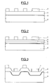
- Figure 1 shows one of these composite samples, before etching, of the stacking of a mask 1 on a silicon layer polycrystalline (or polysilicon) 2 of thickness 200 nm on a layer of silicon oxide 3, called gate oxide, of thickness 4.5 nm on a silicon substrate 4.
- the mask 1 was made of thick silicon oxide 150 nm, and its design included submicron structures (i.e. at least one lateral dimension of which is less than 1 ⁇ m).
- the diameter of the incident beam of the anisotropic reflecting apparatus being of 8 ⁇ m, the analyzed area included different types of structures.
- Figure 2 shows another type of composite sample, before engraving, stacking of a mask 1 identical to that of FIG. 1 on a layer of polysilicon 5 with a thickness of 80 nm on a layer of 120 nm thick polycrystalline germanium 6 on an oxide layer silicon 3 with a thickness of 4.5 nm on a silicon substrate 4.
- the etching of the samples was carried out in a frame of engraving shown in Figure 4, marketed by the company LUCAS LABS, located in Sunnyvale (California, United States).
- the frame was planned to accommodate silicon plates 8 with a diameter of 200 mm. These were fixed on a substrate holder of 9 and their temperature maintained at 35 ° C thanks to cooling by a flow of helium on the rear face.
- the anisotropic reflectance apparatus 10 was installed on the engraving frame as shown in Figure 4.
- a high density plasma source 11 also marketed by Lucas LABS, was used to produce the plasma.
- the gas mixture used was composed of 80 cm 3 of chlorine (Cl 2 ), and 40 cm 3 of oxygen (O 2 ) diluted to 20% in helium (He), under standard conditions.
- the power applied to the source was maintained at 2500 W and the pressure at 267 Pa (2mTorr).
- the power applied to the substrate holder was 400 W for 5 s, in order to remove a thin layer of native oxide on the surface of the polysilicon.
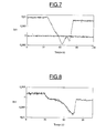
- FIG. 5 represents an anisotropic reflectance signature obtained for the sample represented in FIG. 1, at a wavelength of 280 nm (corresponding to an energy of 4.4 eV).
- the engraving has started in point 12.
- the end of the polysilicon attack was detected by the technique conventional optical emission spectroscopy of plasma, at length 251 nm wave, and corresponds to point 13 on the reflectance signature anisotropic.
- the overprint step was started at this point and lasted 15 s, up to point 14.
- point 13 corresponding to the end of attack of the polysilicon is not a point very easily usable for trigger the no over-etching step. We will see later that we can get signatures where the end of the attack is announced by a sudden variation of ⁇ r / r.
- Step a) the procedure described below was used.
- Signature in Figure 5 obtained at a wavelength of 280 nm, corresponds to step a) of this procedure:
- the point corresponding to the end of the attack a been identified as the transition point between a negative slope and a zero slope, after passing through a successive minimum and maximum.
- Step b) consists, as indicated above, in applying to a sample of the same type the same process, but this time cut into slices of 5 s each, by performing a spectroscopic measurement after each slice, and a real-time measurement at the same wavelength that in a) (280 nm) during each section.
- FIG. 7 represents a signature 20 obtained at a length of 590 nm wave, always for the same type of sample, and a signature 21 obtained at the same wavelength for a sample similar but without mask.
- engraving has started at point 22, and the overprinting step was triggered at point 23.6 s before the end of the polysilicon attack 24.
- the over-etching step lasted another 15 s at from point 24, to point 25.
- the end of the polysilicon attack corresponds to a very rapid variation of ⁇ r / r, easily identifiable, in particular on the derivative, and the no over-etching can be triggered before the end of the attack, for example on the second minimum of ⁇ r / r.
- ⁇ r / r remains zero (at noise measurement), which confirms the fact that the anisotropy measured on the other samples come from the mask structures and their transfer to the polysilicon during the etching.
- FIG. 8 illustrates the case of a sample similar to that of the Figure 1, but with a 1 ⁇ m thick resin mask instead of the oxide mask, the mask design being identical. Optimization of the analysis wavelength led for this sample to a length 280 nm (4.4 eV) wave.
- the end of polysilicon attack polysilicon (point 26) still corresponds to a brutal variation of ⁇ r / r, and the signature can therefore be used to modify the operating conditions of the process.
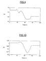
- Figure 9 shows the engraving signature at one length 280 nm waveform for a sample similar to that in Figure 8, but with a different mask design.
- the comparison of figures 8 and 9 shows that the values of ⁇ r / r are larger in absolute terms for the sample in Figure 9, which means that it has a higher strong anisotropy (i.e. more anisotropic structures and / or more strongly anisotropic structures).
- point 27 the end of the attack of polysilicon (point 27) again corresponds to a sudden change in ⁇ r / r.
- the wavelength of 280 nm well suited for resin masks which could be related to the absorption of the resin at this wavelength.
- Figure 10 shows an engraving signature at one length 480 nm (2.6 eV) optimized waveform, for a sample similar to that in Figure 1, but with an oxide mask of the same design as the sample of figure 9.
- the over-etching step was started at the point 29). This last point corresponds to a stabilization of ⁇ r / r, i.e. a cancellation of the derivative.
- Figure 11 shows the etching signature of the sample of Figure 2 at a wavelength of 480 nm. It corresponds to the etching the polysilicon and germanium layers of the sample.
- the over-etching step has been started in point 30, which is the minimum of ⁇ r / r.
- the end of the attack on germanium took place at point 31.8 s after point 30.
- the engraving signature of the sample shown in the figure 3 is given in FIG. 12 for a wavelength of 590 nm.
- This sample included an underlying topography, introducing additional structures.
- the over-etching step was triggered at point 32 of FIG. 12, which corresponds to a rapid variation of ⁇ r / r.
- the end of polysilicon attack (point 33) can be identified by a maximum of ⁇ r / r, and takes place 9 s after point 32.
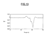
- the last example shown is that of a sample composed of the following stack: mask made of silicon oxide (identical to that of FIGS. 1, 2 and 3) on a layer of polysilicon of thickness 80 nm, on a layer of silicon-germanium polycrystalline alloy (Si 0.45 Ge 0.55 ) of thickness 120 nm, on a layer of silicon oxide of thickness 4.5 nm, on a topography identical to that shown in FIG. 3.
- the signature of the end of attack of such a sample at a wavelength of 590 nm is shown in FIG. 13.
- the over-etching step has been started in point 34, and the end of attack of the alloy has occurred 11 s later in point 35.
- the reflectance signatures anisotropic can be used to control etching processes of sample comprising anisotropic structures. These signatures can be used to modify the operating conditions of plasma to the end of the attack, or even before. Wavelength can be chosen so that the points where we want to modify the conditions of the process correspond to particular points. Of the same way, these signatures can be used to control the thin film deposition processes on anisotropic structures.
Landscapes
- Chemical & Material Sciences (AREA)
- Chemical Kinetics & Catalysis (AREA)
- Engineering & Computer Science (AREA)
- Materials Engineering (AREA)
- Mechanical Engineering (AREA)
- Metallurgy (AREA)
- Organic Chemistry (AREA)
- Physics & Mathematics (AREA)
- General Physics & Mathematics (AREA)
- Drying Of Semiconductors (AREA)
Applications Claiming Priority (2)
| Application Number | Priority Date | Filing Date | Title |
|---|---|---|---|
| FR9715150A FR2771850B1 (fr) | 1997-12-02 | 1997-12-02 | Procede de fabrication de dispositifs en couches minces utilisant la technique de la reflectance anisotrope |
| FR9715150 | 1997-12-02 |
Publications (1)
| Publication Number | Publication Date |
|---|---|
| EP0923121A1 true EP0923121A1 (de) | 1999-06-16 |
Family
ID=9514049
Family Applications (1)
| Application Number | Title | Priority Date | Filing Date |
|---|---|---|---|
| EP98402985A Withdrawn EP0923121A1 (de) | 1997-12-02 | 1998-11-30 | Verfahren zur Herstellung von Dünnschichtvorrichtungen unter Verwendung der anisotropen Reflektionstechnik |
Country Status (2)
| Country | Link |
|---|---|
| EP (1) | EP0923121A1 (de) |
| FR (1) | FR2771850B1 (de) |
Citations (4)
| Publication number | Priority date | Publication date | Assignee | Title |
|---|---|---|---|---|
| JPH02254792A (ja) * | 1989-03-29 | 1990-10-15 | Hitachi Ltd | パターン検出方法及び装置 |
| FR2698443A1 (fr) * | 1992-11-25 | 1994-05-27 | Lyon Ecole Centrale | Procédé et appareil pour mesurer par ellipsométrie la température d'un objet, notamment semi-conducteur. |
| EP0653621A1 (de) * | 1993-11-15 | 1995-05-17 | AT&T Corp. | Verfahren zur Herstellung einer Vorrichtung unter Verwendung einer Ellipsometrietechnik |
| EP0768512A2 (de) * | 1995-10-16 | 1997-04-16 | Lucent Technologies Inc. | Fabrikationsverfahren mit polarisiertem Licht zum Determinieren der Dicke von Dünnschichten |
-
1997
- 1997-12-02 FR FR9715150A patent/FR2771850B1/fr not_active Expired - Fee Related
-
1998
- 1998-11-30 EP EP98402985A patent/EP0923121A1/de not_active Withdrawn
Patent Citations (4)
| Publication number | Priority date | Publication date | Assignee | Title |
|---|---|---|---|---|
| JPH02254792A (ja) * | 1989-03-29 | 1990-10-15 | Hitachi Ltd | パターン検出方法及び装置 |
| FR2698443A1 (fr) * | 1992-11-25 | 1994-05-27 | Lyon Ecole Centrale | Procédé et appareil pour mesurer par ellipsométrie la température d'un objet, notamment semi-conducteur. |
| EP0653621A1 (de) * | 1993-11-15 | 1995-05-17 | AT&T Corp. | Verfahren zur Herstellung einer Vorrichtung unter Verwendung einer Ellipsometrietechnik |
| EP0768512A2 (de) * | 1995-10-16 | 1997-04-16 | Lucent Technologies Inc. | Fabrikationsverfahren mit polarisiertem Licht zum Determinieren der Dicke von Dünnschichten |
Non-Patent Citations (1)
| Title |
|---|
| PATENT ABSTRACTS OF JAPAN vol. 014, no. 584 (E - 1018) 27 December 1990 (1990-12-27) * |
Also Published As
| Publication number | Publication date |
|---|---|
| FR2771850A1 (fr) | 1999-06-04 |
| FR2771850B1 (fr) | 2001-06-08 |
Similar Documents
| Publication | Publication Date | Title |
|---|---|---|
| EP1121580B1 (de) | Vorrichtung zur optischen charakterisierung eines dünnschichtmaterials | |
| WO2010049652A9 (fr) | Dispositif et procede de mesures polarimetriques spectroscopiques dans le domaine visible et proche infrarouge | |
| EP0663590B1 (de) | Moduliertes Spektralellipsometer | |
| JP3790628B2 (ja) | 膜厚及び光学定数の測定方法及び装置 | |
| FR2776375A1 (fr) | Methode de caracterisation d'un processus d'implantation ionique | |
| CN111076668B (zh) | 用于纳米厚度SiO2厚度的差分反射光谱测量方法 | |
| US5929995A (en) | System and method for directing electromagnetic beams | |
| EP0332508A1 (de) | Apparat zur ellipsometrischen Untersuchung, Verfahren zur ellipsometrischen Untersuchung einer Probe, Verwendung zur Messung der Dickenänderung dünner Schichten | |
| EP0843889A1 (de) | Vorrichtung und verfahren zur laser-oberflächenbehandlung | |
| EP0294873A1 (de) | Testvorrichtung zur Durchführung eines Realisierungsverfahrens von Halbleiterstrukturen | |
| EP0237415B1 (de) | Vorrichtung zur spektralphotometrischen Ellipsometrie mit Verwendung optischer Fasern | |
| EP0466598A1 (de) | Verfahren und Einrichtung zur Ablagerung von Antireflektionsschichten und zur Kontrolle ihrer Dicke | |
| FR2737779A1 (fr) | Dispositif ellipsometre a haute resolution spatiale | |
| EP0045674B1 (de) | Verfahren und Vorrichtung zum Ätzen einer dünnen Schicht mit einem Plasma | |
| EP0923121A1 (de) | Verfahren zur Herstellung von Dünnschichtvorrichtungen unter Verwendung der anisotropen Reflektionstechnik | |
| EP0670993B1 (de) | Verfahren und vorrichtung zum messen der temperatur eines objektes, besonders eines halbleiters, mittels ellipsometrie | |
| WO2005026707A2 (fr) | Utilisation de la transformee de fourier optique pour le controle dimensionnel en microelectronique | |
| EP1086355B1 (de) | Ellipsometrisches verfahren und kontrollvorrichtung zur herstellung eines dünnschichtbauelements | |
| EP1579197B1 (de) | Verfahren zur optischen charakterisierung von materialen ohne verwendung eines physikalischen modells | |
| JP2917938B2 (ja) | 偏光解析方法および偏光解析装置 | |
| EP1179729A1 (de) | Verfahren zur Echtzeitkontrolle der Herstellung einer Dünnschichtstruktur durch ellipsometrische Messung | |
| Hilfiker et al. | Recent developments in spectroscopic ellipsometry for materials and process control | |
| WO2002037086A1 (fr) | Procede d'analyse quantitative et selective des composes contaminants volatils dans un melange gazeux par spectroscopie infrarouge | |
| CN113466141A (zh) | 一种用椭圆偏振光谱仪无损检测金属衬底氧化变性的方法 | |
| JP2025030847A (ja) | 試料分析方法及び試料分析装置 |
Legal Events
| Date | Code | Title | Description |
|---|---|---|---|
| PUAI | Public reference made under article 153(3) epc to a published international application that has entered the european phase |
Free format text: ORIGINAL CODE: 0009012 |
|
| AK | Designated contracting states |
Kind code of ref document: A1 Designated state(s): DE GB NL |
|
| AX | Request for extension of the european patent |
Free format text: AL;LT;LV;MK;RO;SI |
|
| 17P | Request for examination filed |
Effective date: 19991111 |
|
| AKX | Designation fees paid |
Free format text: DE GB NL |
|
| 17Q | First examination report despatched |
Effective date: 20060802 |
|
| STAA | Information on the status of an ep patent application or granted ep patent |
Free format text: STATUS: THE APPLICATION IS DEEMED TO BE WITHDRAWN |
|
| 18D | Application deemed to be withdrawn |
Effective date: 20061213 |