EP0923263A2 - Système de communitation des paquets optiques et commutateur optique - Google Patents
Système de communitation des paquets optiques et commutateur optique Download PDFInfo
- Publication number
- EP0923263A2 EP0923263A2 EP98123440A EP98123440A EP0923263A2 EP 0923263 A2 EP0923263 A2 EP 0923263A2 EP 98123440 A EP98123440 A EP 98123440A EP 98123440 A EP98123440 A EP 98123440A EP 0923263 A2 EP0923263 A2 EP 0923263A2
- Authority
- EP
- European Patent Office
- Prior art keywords
- optical
- packet
- address
- circuit
- electrical
- Prior art date
- Legal status (The legal status is an assumption and is not a legal conclusion. Google has not performed a legal analysis and makes no representation as to the accuracy of the status listed.)
- Granted
Links
Images


Classifications
-
- H—ELECTRICITY
- H04—ELECTRIC COMMUNICATION TECHNIQUE
- H04Q—SELECTING
- H04Q11/00—Selecting arrangements for multiplex systems
- H04Q11/0001—Selecting arrangements for multiplex systems using optical switching
-
- H—ELECTRICITY
- H04—ELECTRIC COMMUNICATION TECHNIQUE
- H04L—TRANSMISSION OF DIGITAL INFORMATION, e.g. TELEGRAPHIC COMMUNICATION
- H04L49/00—Packet switching elements
- H04L49/30—Peripheral units, e.g. input or output ports
-
- H—ELECTRICITY
- H04—ELECTRIC COMMUNICATION TECHNIQUE
- H04L—TRANSMISSION OF DIGITAL INFORMATION, e.g. TELEGRAPHIC COMMUNICATION
- H04L49/00—Packet switching elements
- H04L49/50—Overload detection or protection within a single switching element
-
- H—ELECTRICITY
- H04—ELECTRIC COMMUNICATION TECHNIQUE
- H04L—TRANSMISSION OF DIGITAL INFORMATION, e.g. TELEGRAPHIC COMMUNICATION
- H04L49/00—Packet switching elements
- H04L49/25—Routing or path finding in a switch fabric
-
- H—ELECTRICITY
- H04—ELECTRIC COMMUNICATION TECHNIQUE
- H04Q—SELECTING
- H04Q11/00—Selecting arrangements for multiplex systems
- H04Q11/0001—Selecting arrangements for multiplex systems using optical switching
- H04Q11/0005—Switch and router aspects
- H04Q2011/0007—Construction
- H04Q2011/0024—Construction using space switching
-
- H—ELECTRICITY
- H04—ELECTRIC COMMUNICATION TECHNIQUE
- H04Q—SELECTING
- H04Q11/00—Selecting arrangements for multiplex systems
- H04Q11/0001—Selecting arrangements for multiplex systems using optical switching
- H04Q11/0005—Switch and router aspects
- H04Q2011/0037—Operation
- H04Q2011/0039—Electrical control
-
- H—ELECTRICITY
- H04—ELECTRIC COMMUNICATION TECHNIQUE
- H04Q—SELECTING
- H04Q11/00—Selecting arrangements for multiplex systems
- H04Q11/0001—Selecting arrangements for multiplex systems using optical switching
- H04Q11/0005—Switch and router aspects
- H04Q2011/0037—Operation
- H04Q2011/0045—Synchronisation
-
- H—ELECTRICITY
- H04—ELECTRIC COMMUNICATION TECHNIQUE
- H04Q—SELECTING
- H04Q11/00—Selecting arrangements for multiplex systems
- H04Q11/0001—Selecting arrangements for multiplex systems using optical switching
- H04Q11/0005—Switch and router aspects
- H04Q2011/0037—Operation
- H04Q2011/005—Arbitration and scheduling
Definitions
- the optical/electrical converter is usually of an ac coupling circuit configuration.
- the optical/electrical converter is usually of an ac coupling circuit configuration.
- This dummy packet is a pattern which is made up of at least one bit of 0 and the same number of bit of 1, with 0 or 1 not continuing for longer than a pre-set time, and to which is appended a particular code by which the packet can be judged to be a dummy packet.
- An output unit includes a dummy packet eliminating circuit which discriminates a dummy packet based on the possible presence of the particular code specifying a dummy packet to eliminate the discriminated dummy packet in order to receive only the necessary packets.
- a contention resolution circuit is used in order to inhibit packet interference due to arrival of plural packets at the same output unit, which would lead to reception of erroneous data.
- the contention resolution circuit selects a sole input unit from the plural input units to give the input unit a permission for connection. The remaining input units are inhibited from connection. Since the input units inhibited as to connection are equivalent to the input units devoid of the packets for transmission, these input units send dummy packets.
- the contention resolution circuit has to detect an input unit devoid of the packets for transmission and an output unit devoid of packets for reception and to find out a connection pattern to interconnect these input and output units.
- Fig.37 shows a configuration of a conventional optical switch used in an exchange stage.
- this optical switch is a 4-input 4-output splitter/combiner type optical switch having four light splitters 10, 16 optical gates 11 and four light combiners 12.
- 4 2 or 16 control lines are required to control the 16 optical gates.
- the sending station In sending packets from a sending station to the exchange apparatus, the sending station transmits, along with a packet(s), a destination address specifying the receiving station to receive the packet(s), to the exchange apparatus. In the absence of packets to be transmitted in the input unit, no designation of the destination address is made from the transmitting station to the input unit.
- a contention resolution circuit searches an input unit devoid of a packet(s) to be transmitted and an output unit devoid of a packet(s) to be received and controls the optical switch driving circuit for interconnecting these input and output units.
- the exchange apparatus is increased in the circuit scale. If the network speed is increased, it becomes impossible to control the exchange apparatus at a high speed.
- the dummy packet is deemed in the receiving station as being unnecessary or erroneous data, it is necessary to provide a dummy packet eliminating system in order to prevent the dummy packet from being output from the exchange apparatus to the receiving station.
- the special code specifying a dummy packet appended to the dummy packet is detected for eliminating the dummy packet. That is, in case where a packet other than the dummy packet is received as a substitute for the dummy packet in order to avoid mulfunction of an O/E converter of an output unit inherently having no packet to be received, the dummy packet eliminating system cannot eliminate this packet as an invalid packet and erroneously sends this packet to the reception station.
- an output unit devoid of the packet to be received has to be connected to an input unit transmitting a dummy packet, that is to an input unit devoid of the packet to be transmitted, such that it becomes necessary to search and connect input and output units sending and receiving the dummy packet expeditiously.
- Another problem is the interconnection for control signals for the optical switch. That is, if the optical switch is increased in scale, the control signal lines between the optical switch and the control circuits are increased in volume and structure thus causing congestion of the control signal lines.
- control signal lines For example, if, in the case of a 128 by 128 line full-cross bus switch, a bit map of the switch connection pattern is formulated in the control circuit and a control signal is sent to the optical switch, 128 2 or 16384 control lines are required. Since these numerous control signal lines affect mounting of the exchange apparatus or optical switches, it is incumbent to reduce the number of the control signal lines.
- An optical packet exchange apparatus includes (a) a plurality of input devices having input buffer means (units), parallel/serial conversion means (units), electrical/optical conversion means (units), and dummy packet insertion means (units) for sending a dummy packet if there is no packet to be transmitted.
- the apparatus further includes (b) exchange counterpart contention resolution means (units) for controlling an exchange counterpart, (c) a plurality of output devices having optical/electrical conversion means (units), serial/parallel conversion means (units) and packet eliminating means (units), and (d) an optical switch (e) wherein the packets are exchanged, and (f) wherein the exchange counterpart contention resolution means (units) controls the packet eliminating means to eliminate the dummy packet.
- the packet exchange apparatus is characterized in that the dummy packet inserting means includes a dummy packet generating circuit, a selector circuit and a packet readout circuit for controlling the selector circuit and the input buffer means.
- the packet exchange apparatus is characterized in that the dummy packet inserting means is an encoding circuit and the dummy packet eliminating means is a decoding circuit.
- a packet exchange apparatus includes (a) a plurality of input devices having input buffer means, parallel/serial conversion means and electrical/optical conversion means, (b) a dummy packet inputting device for transmitting a dummy packet, (c) exchange counterpart contention resolution means for controlling an exchange counterpart, (d) a plurality of output devices having optical/electrical conversion means, serial/parallel conversion means and packet eliminating means, and (e) an optical switch; and (f) the exchange counterpart contention resolution means controls the packet eliminating means to eliminate the dummy packet.
- a packet exchange apparatus includes (a) a plurality of input devices having input means, parallel/serial conversion means, electrical/optical conversion means, and dummy packet insertion means for sending a dummy packet if there is no packet to be transmitted, (b) exchange counterpart contention resolution means for controlling an exchange counterpart, (c) a plurality of output devices having optical/electrical conversion means, serial/parallel conversion means and packet eliminating means, and (d) an optical switch. (e) The output device includes an address comparator circuit for controlling the packet eliminating means based on results of comparison of the destination address of the received packet to an address allocated to the output device.
- the dummy packet inserting means includes a dummy packet generating circuit, a selector circuit and a packet readout circuit for controlling the selector circuit and the input buffer means.
- dummy packet inserting means is an encoding circuit and the dummy packet eliminating means is a decoding circuit.
- the destination address in the dummy packet is set to an address other than the address allocated to the connected output device.
- a packet exchange apparatus includes (a) a plurality of input devices having input buffer means, parallel/serial conversion means and electrical/optical conversion means; (b) a dummy packet inputting device for transmitting a dummy packet; (c) exchange counterpart contention resolution means for controlling an exchange counterpart; (d) a plurality of output devices having optical/electrical conversion means, serial/parallel conversion means and packet eliminating means; and (e) an optical switch.
- the output device includes an address comparison circuit which controls the packet eliminating means from the results of comparison of a destination address of a received packet to an address allocated to the output device.
- the destination address in the dummy packet is set to an address other than the address allocated to the connected output device.
- a packet exchange apparatus includes (a) a plurality of input devices having input buffer means, parallel/serial conversion means, electrical/optical conversion means, and dummy packet insertion means for sending a dummy packet if there is no packet to be transmitted; (b) exchange counterpart contention resolution means for controlling an exchange counterpart; (c) a plurality of output devices having optical/electrical conversion means, serial/parallel conversion means, packet eliminating means and dummy packet code detection means for detecting a code specifying a dummy packet to control the packet eliminating means; and (d) an optical switch. It is characterized by further including (e) a dummy packet destination address calculating circuit setting a connection pattern so that different input devices output dummy packets to respective non-selected output devices.
- dummy packet inserting means includes a dummy packet generating circuit, a selector circuit and a packet readout circuit controlling the selector circuit and the input buffer means.
- dummy packet inserting means is an encoding circuit and the dummy packet eliminating means is a decoding circuit.
- an optical packet exchange apparatus includes (a) a plurality of input devices having input buffer means, parallel/serial conversion means, electrical/optical conversion means and dummy packet insertion means for sending a dummy packet if there is no packet to be transmitted; (b) exchange counterpart contention resolution means for controlling an exchange counterpart; (c) a plurality of output devices having optical/electrical conversion means, serial/parallel conversion means, packet eliminating means and dummy packet code detection means for detecting a code specifying a dummy packet to control the packet eliminating means; (d) an optical switch.
- a dummy packet sender addresses calculating circuit for setting a connection pattern so that a non-selected output device (unit) will receive a dummy packet from at least one input device (unit) having no packet to be transmitted.
- dummy packet inserting means includes a dummy packet generating circuit, a selector circuit and a packet readout circuit controlling the selector circuit and the input buffer means.
- dummy packet inserting means is an encoding circuit and the dummy packet eliminating means is a decoding circuit.
- an optical packet exchange apparatus includes : (a) a plurality of input devices having input buffer means, parallel/serial conversion means and electrical/optical conversion means; (b) a dummy packet input device transmitting a dummy packet; (c) exchange counterpart contention resolution means for controlling an exchange counterpart; (d) a plurality of output devices having optical/electrical conversion means, serial/parallel conversion means and packet eliminating means; and (e) an optical switch, (f) wherein the output device includes a dummy packet code detection circuit detecting a code specifying a dummy packet, for controlling the packet eliminating means, and (g) wherein an output device having no packet to be received is connected to the dummy packet input device.
- an optical switch includes (a) a plurality of transmitters having variable wavelength electrical/optical converting means and address decoding means; (b) optical combining/splitting means; and (c) a plurality of receivers (reception devices) having fixed wavelength filter means and optical/electrical converting means, and is characterized by further including (d) an address conversion circuit converting an address to be accorded to the address decoding means from a sender address for a receiver to a destination address for a transmitter (sender device).
- an optical switch includes (a) a plurality of transmitters having fixed wavelength electrical/optical conversion means having different wavelengths allocated to different transmitters; (b) optical combining/splitting means; (c) a plurality of receivers having wavelength selection means, optical/electrical converting means and address decoding means; and further including (d) an address conversion circuit converting an address to be accorded to the address decoding means from a destination address for a transmitter to a sender address for a receiver.
- N and M being integers not less than 2;
- M - number of N x K - optical spatial switch means for switching paths of N optical output signals of one group of the variable wavelength electrical/optical converting means, K being an integer not less than 2;
- K - number of optical combining/splitting means for combining optical signals from respective different output ports of the M - number of N x K - optical spatial switch means for splitting the combined signal into M - number of outputs;
- MK - number of optical/electrical converting means are integers not less than 2;
- the optical spatial switch includes (f1) N - number of optical splitting means branched into K branches, (f2) optical gate means for turning optical signals branched by the optical splitting means on/ off, and (f3) K - number of optical combining means for combining optical signals from K - number of different optical branching means.
- the optical switch further includes address decoding means for controlling the variable wavelength electrical/optical converting means and one of the optical gate means connected to the optical splitting means.
- address conversion means for converting a sender address for a receiver to a destination address for a transmitter to enter the converted destination address to the address decoding means.
- an optical switch includes; (a) K groups of fixed wavelength electrical/optical converting means, each of the groups having M - number of fixed wavelength electrical/optical converting means to which are allocated M different wavelengths ⁇ 1, ⁇ 2,..., ⁇ M, M and K being integers not less than 2; (b) K - number of optical combining/splitting means for combining M - number of optical outputs of one group of the fixed wavelength electrical/optical converting means and for branching the combining signal into M branches; (c) M - number of K x N optical spatial switch means having outputs of K different optical combining/splitting means as inputs, N being an integer not less than 2; (d) MN - number of wavelength selecting means for selecting an optical signal of any wavelength from the outputs of the optical spatial switch means, to output the selected signal; and (e) MN - number of optical/electrical converting means.
- the optical spatial switch means has (f1) K - number of optical splitting means branched into N branches, (f2) optical gate means for turning the optical signals branched by the optical splitting means on/off, and (f3) N - number of optical combining means for combining optical signals branched by the K different optical branching means. (g) There is further provided address decoding means for controlling one of the optical gate means connected to the optical combining means and the wavelength selecting means by a sender address for a receiver.
- address conversion means for converting a destination address for a transmitter to a sender address for a receiver to supply the converted destination address to the address decoding means.
- An optical packet exchange apparatus includes plural input devices (101 of Fig.1), an exchange counterpart contention resolution means (103 of Fig.1), plural output devices (102 of Fig.1), an optical switch (100 of Fig.1) and an optical switch control means (104 of Fig.1).
- Each input device is made up of an input buffer means (107 of Fig.2), parallel/serial converting means (111 Of Fig.2), an electro-optical converting means (112 of Fig.2) and a dummy packet insertion means (108 of Fig.2) for transmitting a dummy packet in the absence of packets for transmission.
- the exchange counterpart contention means controls the partner (or destination) of exchange.
- Each output device is made up of an optical/electrical converting means (113 of Fig.3), serial/parallel converting means (114 of Fig.3) and packet eliminating means (115 of Fig.3).
- the exchange counterpart contention resolution means (103 of Fig.1) judges contention among respective output devices, from a destination address and a connection request signal from the input device, sets a connection pattern (or mode) for an optical switch from the result of contention resolution, sends an optical switch control signal to optical switch control means (104 of Fig.1) and sets a connection pattern for connecting an output device not required for connection to any one of the input devices.
- the optical switch control means controls the optical switch in accordance with the connection pattern to connect the input and output devices.
- the exchange counterpart contention resolution means (103 of Fig.1) sends a packet discarding control signal to packet eliminating means (115 of Fig.3) of an output device not required for connection to eliminate the dummy packet.
- Transmission packets sent from a sender station are buffered in the input devices. Every input device sends a destination address and a connection request signal to the exchange counterpart contention resolution means.
- the exchange counterpart contention resolution means judges contention among the output devices, from the destination addresses and the connection request signals from the input devices, and sends a connection permission signal to an input device which won the contention without sending the connection permission signals to an input device which lost the contention or which has sent no connection request signal.
- the input device which received the connection request signal outputs a transmission packet to the optical switch.
- the input device which has received no connection permission signal selects outputting of the dummy packet insertion means, while it buffers the transmission packet, and outputs the dummy packet to the optical switch.
- the exchange counterpart contention resolution means sets an optical switch connection pattern (mode) from the result of decision of contention and sends an optical switch control signal to the optical switch control means, while setting a connection pattern to an output device not required to be connected so that this output device will be connected to any one of the input devices.
- the optical switch control means controls (governs connection of) the optical switch in accordance with a connection pattern as set to interconnect input and output devices.
- the exchange counterpart contention resolution means sends a packet discarding signal to an output device not required to be connected so that the output device not required to be connected is connected to some input device to receive a dummy packet or a packet addressed to another output device.
- the packet eliminating means of the output device On reception of a packet discarding signal from the exchange counterpart contention resolution means, the packet eliminating means of the output device deems that the received packet is not addressed to itself and discards same. Thus, there is no risk of delivery of packets or dummy packets addressed to anther reception station to the reception station under consideration to realize normal exchange operations.
- an optical switch of the present invention includes plural transmitters having variable wavelength electrical/optical converting means (860 of Fig.20) and address decoding means (861 of Fig.20), and a plurality of receivers (receivers), having optical combining/splitting means (864 of Fig.20), fixed wavelength filter means (862 of Fig.20) and optical/electrical converting means (O/E 863 of Fig.20), in which there is further provided an address conversion circuit (865 of Fig.20) for converting an address to be accorded to the address decoding means from a sender address for a receiver to a destination address for a transmitter.
- an optical switch of the present invention includes a plurality of transmitters comprised of fixed wavelength electrical/optical converting means E/O(866 of Fig.21) having different wavelengths allocated to respective transmitters and a plurality of receivers comprised of optical combining/splitting units (864 of Fig.21), optical/electrical converting means (863 of Fig.21) and an address decoder (868 of Fig.21), in which there is further provided address conversion means (865 of Fig.21) for converting an address to be accorded to address decoding means from a destination address for a transmitter to a sender address for a receiver.
- an optical switch of the present invention includes the followings:
- Fig.1 shows the configuration of the first example of the present invention.
- the preset example is an optical packet exchange apparatus in which the second aspect of the invention is applied to the first aspect of the invention and comprised of the input side of four channels and the reception side of four channels.
- the optical packet exchange apparatus includes four input units 101, an optical switch 100, four output units 102, a contention resolution circuit 103 , and an optical switch control circuit 104 .
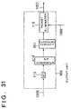
- Fig.37 shows an illustrative structure of an optical switch 100.
- the optical switch 100 is a splitter/combiner type optical switch of four input channels and four output channels comprised of four optical splitters 10, 16 optical gates 11 and four optical combiners 12.
- the optical gate 11 is a semiconductor light amplifier which, upon application of current, is turned on to transmit light signals and which, upon non-applying current, is turned off to interrupt light signals.
- the input light signals are split (branched) into four by the optical splitters 10 to fall on the four optical gates 11 connected in circuit.
- the optical switch 100 can switch the route (optical path) of the light signal entered via the input port by the control signal to output the switched light signal at an optional output port.
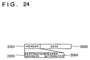
- Fig.24 shows an illustrative data format of a packet exchanged by the packet exchange apparatus.
- the packet is made up of a header part 2001, composed of the destination address information 2003 and the header attribute information 2004, and a data part 2002.
- the transmission packet sent from a sending station, is buffered by input units 101.
- Each of the input units 101 sends a destination address 1003 of the transmission packet and a connection request signal 1004 to a comprehensive contention resolution circuit 103.
- the contention resolution circuit 103 receives destination addresses 1003-1 to- 4 and connection request signals 1004-1 to -4 from the input units 101-1 to -4 and judges contention as to the output units 102-1 to -4 to send a connection permission signal 1005-1 to -4 to any of the input units which has won the contention, respectively.
- the contention resolution circuit 103 does not send the connection permission signals 1005 to the input units which have lost the contention or which have not sent the connection request signals.
- connection permission signal 1005 Any of the inputs unit 101 which has received the connection permission signal 1005 outputs the transmission packet to the optical switch 100.
- the input unit 101 which has not received the connection permission signal 1005 outputs a dummy packet to the optical switch 100 while buffering the transmission packet.
- the contention resolution circuit 103 sets a connection pattern for the optical switch 100 based on the results of decision of the contention to send an optical switch control signal 1009 to the optical switch control circuit 104, while setting another connection pattern to connect any of output units 102, for which the connection request has not been made, to one of the input units 101.
- the optical switch control circuit 104 controls the optical switch 100 in accordance with the applied connection pattern to interconnect the input unit 101 and the output unit 102.
- the contention resolution circuit 103 sends a packet discarding signal 1008 to the output unit 102 for which the connection request has not been made.
- the output unit 102 for which the connection request has not been made, is connected to one of the input units 101 to receive the dummy packet or a packet addressed to another output unit.
- the output unit 102 can discard the received packet based on judgment that the received packet is not a packet addressed to the output unit 102 concerned.
- the exchange operation can be performed regularly without delivery through error to a receiving station under consideration of a packet addressed to another receiving station or dummy packet.
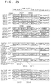
- Fig.25 shows, by way of an example, an exchange operation of 4-time slot time in case of sending packets from four sending stations to four receiving stations.
- a destination 1 represents the number of a receiving station, that is a destination address
- data A represents transmission data of the packet.
- NO PACKET at 2006 represents a time slot in which no packet has been sent from the sending station.
- a packet 2005 and a packet 2007, addressed in the first time slot to the same output station 1, are entered to the input unit 1 and to the input unit 2, respectively.
- the contention resolution circuit 103 judges contention between the (two) packets 2005 and 2007 to accord a connection permission signal to the input unit 1 which then outputs the packet 2005, whereas the input unit 2 outputs a dummy packet.
- the packet 2007 acquires a connection permission signal in the second time slot so as to be output as packet 2009. (Second paragraph)
- packets are output to the destinations 1, 2 and 3. However, there is no packet addressed to destination 4. If there is no packet to be received by the output unit, a command is issued to connect the output unit 1 to any one of the input units.
- a command is issued to connect the output unit 1 to the input unit 1, to connect the output unit 2 to the input unit 2, to connect the output unit 3 to the input unit 3, and to connect the output unit 4 to the input unit 4. That is, if there is no packet addressed to the destination 4, the output unit 4 is connected to the input unit 4 so that a packet 2010 is entered. Since the contention resolution circuit 103 accords a packet discarding signal 2012 to the output unit 4, the output unit 4 discards the packet 2010 so that the output to the output unit 4 is NO PACKET at 2013.
- the output unit 4 is similarly connected to the input unit 4 to receive a dummy packet 2011 which, however, is discarded, so that an output to the output unit 4 is NO PACKET at 2014.
- the output unit devoid of the packet to be received is connected to the input unit of the same number. However, it is optional to which input number connection is to be made such that connection may be made to a particular input unit. If all output units having no packet to be received are connected to the same input unit, it is unnecessary for the remaining input units to output dummy packets for achieving stable operation of the output units. However, dummy packets may be output for stable operation of the input units or the optical switch.
- time slots for inputs of the input units, outputs from the input units, inputs of the output units and outputs from the output units are shown in an aligned state for convenience.
- the temporal positions of the respective time slots are deviated slightly due to processing delay in the various portions or signal propagation delay.
- Fig.2 shows an illustrative structure of an input unit 101 in the present example.
- the input unit 101 in the preset example is made up of a destination address extraction circuit 105, a dummy packet generating circuit 106, an input packet buffer 107, a selector 108, an address buffer 109, a packet readout circuit 110, a parallel/serial converter 111 and an electro-optical converter 112.
- the destination address extraction circuit 105 extracts a destination address of an input packet signal 1001 to buffer the address at the address buffer 109 while buffering the packet at the input packet buffer 107.
- the address buffer 109 outputs a destination address signal 1003 and a connection request signal 1004 to the contention resolution circuit.
- the packet readout circuit 110 On reception of the connection permission signal 1005 from the contention resolution circuit 103 (see Fig.1), the packet readout circuit 110 erases a corresponding address in the address buffer 109, while taking out a corresponding packet from the input packet buffer 107 to control the selector to output the packet to the parallel/serial (P/S) converter 111.
- P/S parallel/serial
- the parallel/serial converter 111 parallel/serially converts the packet signal.
- the electro-optical converter (E/O) 112 converts the serial signals into a light signal 1002 which is output to the optical switch.
- the packet readout circuit 110 controls the selector 108, without moving the information in the address buffer 109 and the input packet buffer 107, in order to output the dummy packet generated by the dummy packet generating circuit 106 to the parallel/serial converter 111.
- This dummy packet is converted by the parallel/serial converter 111 and the electro-optical converter 112 into a light signal 1002 which is output to the optical switch 100 (see Fig.1).
- Fig.3 shows an illustrative structure of a sole output unit 102 in the present example.
- the output unit 102 is made up of an optical/electrical converter 113, a serial/parallel (S/P) converter 114 and a packet eliminating circuit 115.
- the light signal 1006, supplied from the optical switch 100 (see Fig.1), is converted by the optical/electrical converter 113 into electrical signals and converted by the serial/parallel converter 114 to parallel signals which are fed to the packet eliminating circuit 115.
- the packet discarding signal 1008 is sent by the contention resolution circuit 103 (see Fig.1) to the packet eliminating circuit 115, the packet is discarded, with an output packet signal 1007 being then a packet absent signal. In the absence of the packet discarding signal 1008, the packet signal received at the output packet signal 1007 is output.
- Fig.4 shows an illustrative structure of the contention resolution circuit 103.
- the contention resolution circuit 103 is made up of address decoders 116-1 to -4, conciliation circuits 117-1 to -4, OR gates 118-1 to-4, address encoders 119-1 to-4, address generators 120-1 to -4 and selectors 121-1 to- 4.
- the address decoder 116 On reception of a destination address signal 1003 and a connection request signal 1004, the address decoder 116 decodes the destination address to send a connection request signal to the reconciliation circuit 117 associated (corresponding) with the destination.
- the reconciliation circuit 117 receives a connection request signal for connecting to an output unit associated with the reconciliation circuit from each input unit to determine to which of the input units required for connection should be accorded, followed by outputting a connection permission signal to the OR gate 118 and to the address encoder 119.
- the OR gate 118 ORs the connection permission signals associated with the respective input units of the reconciliation circuits to accord the connection permission signals 1005 to the respective input units.
- the address encoder 119 encodes a connection permission signal from one of the reconciliation circuit 117 into an address to acquire an address of the input unit to which each output unit should be connected. This address is output as an optical switch control signal 1009 via selector 121 to an optical switch control circuit.
- the reconciliation circuit 117 controls the selector 121 based on the selector control signal to output an address generated by the address generator 120 as an optical switch control signal 1009 to the optical switch control circuit while according a selector control signal as a packet discarding signal 1008 to a corresponding output unit.
- Fig.5 shows the structure of the second example.
- This example is directed to an optical packet exchange apparatus for the 4 transmission channels and 4 reception channels practicing the fourth aspect of the present invention.
- the packet exchange apparatus is comprised of four input units 201, an optical switch 100, four output units 202, a contention resolution circuit 103, an optical switch control circuit 104 and a dummy packet input unit 222.
- the input units 201 each send a destination address 1003 of the transmission packet and a connection request signal to the contention resolution circuit 103.
- the contention resolution circuit 103 receives the destination addressed 1003-1 to -4 and the connection request signals 1004-1 to -4 from the respective input units 201-1 to -4 to judge the contention for the output units 102-1 to -4 to send connection permission signals 1005-1 to -4 to any of the input units that won the contention.
- no connection permission signal is sent by the contention resolution circuit 103.
- the input unit 201 that has received the connection permission signal 1005 outputs a transmission packet to the optical switch 100.
- the input unit 201 that has received no connection permission signal 1005 keeps the transmission packet buffered.
- the contention resolution circuit 103 sets a connection pattern of the optical switch 100 from the results of the judgment of contention and sends an optical switch control signal to the optical switch control circuit 104, while setting a connection pattern to the output unit 102 not required for connection so that the output unit(s) 102 will be connected to the dummy packet input unit 222.
- the contention resolution circuit 103 sends a packet discarding signal 1008 to the output unit(s) 102 not required for connection.
- any of the output units 102 is connected to the dummy packet input unit 222 to receive a dummy packet. It is noted that, on reception of the packet discarding signal 108 from the contention resolution circuit 103, the output unit 102 can discard a received packet based on judgment that the received packet is not addressed to itself. Thus, the exchange operation can be executed regularly without a dummy packet being erroneously sent to the receiving station.
- a 4-by-4 (4 x 4) optical switch 100 operates in the same manner as the 4-by-4 optical switch 100 of the first example.
- the destination address extraction circuit 205 extracts a destination addresses of the input packet signal 1001 to buffer the address in the address buffer 209 and to buffer packets in the input packet buffer 207.
- the address buffer 209 outputs a destination address signal 1003 and a connection request signal 1004 to the contention resolution circuit.
- the packet readout circuit 210 does not move the information in the address buffer 209 or in the input packet buffer 207.
- the input packet buffer 207 is not required to make any output, it is also possible for the input packet buffer 207 to output an optional pattern for stabilization of the electro-optical converter 212 or the optical switch, then to convert the pattern by parallel/series conversion by the parallel/serial converter 211, and to convert the converted pattern to an optical signal 1002 which is output to the optical switch.
- a dummy packet data generated by the dummy packet generator 223 is fed to the optical switch 100 as a light signal converted to a serial signal by the parallel/serial converter 211 and the electro-optical converter 212.
- Fig.3 shows an illustrative structure of a sole output unit 102 in the present example.
- an output unit identified with the output unit 102 explained with reference to the first example is used. That is, referring to Fig.3, the output unit 102 is made up of an optical/electrical converter 113, a serial/parallel converter 114 and a packet eliminating circuit 115.
- a packet discarding signal 1008 is sent to the packet eliminating circuit 115 by the contention resolution circuit 103 (see Fig.5), the packet is discarded and the output packet signal is devoid of packet. If no packet discarding signal 108 is sent, the received packet signal is output as an output packet signal 1007.
- Fig.4 shows an illustrative structure of the contention resolution circuit 103.
- the contention resolution circuit 103 is made up of address decoders 116-1-4, conciliation circuits 117-1 to -4, OR gates 118-1 t o-4, address encoders 119-1 t o4, address generators 120-1 to -4 and selectors 121-1 to -4.
- the address decoder 116 decodes the destination address to send a connection request signal to the reconciliation circuit 117 (see Fig.5) associated with the destination.
- the reconciliation circuit 117 receives the connection request signal to the output unit associated with the reconciliation circuit from each of the input units to determine to which of the input units required for connection the connection permission should be accorded to output a connection permission signal to the OR gate 118 and to the address encoder 119.
- the OR gate 18 logically sums the connection permission signals associated with the respective input units of the reconciliation circuits to accord a connection permission signal 1005 to the respective input units.
- the address encoder 119 encodes the connection permission signal from one of the reconciliation circuits 117 into an address to acquire an address of the input unit to which respective output unit should be connected. This address is output as an optical switch control signal 1009 via selector 121 to an optical switch control circuit.
- the reconciliation circuit 117 controls the selector 121 by a selector control signal to output the address of the dummy packet input unit 222 generated by the address generator 120 as an optical switch control signal 1009 to the optical switch control circuit.
- the reconciliation circuit 117 also accords a selector control signal as a packet discarding signal 1008 to an associated output unit.
- Fig.8 shows the structure of the third example.
- This example is directed to an optical packet exchange apparatus for the 4 transmission channels and 4 reception channels practicing the fifth aspect of the present invention to which the sixth and eighth aspects of the invention have been applied.
- the packet exchange apparatus is comprised of four input units 101, an optical switch 100, four output units 302, a contention resolution circuit 103, and an optical switch control circuit 104.
- the transmission packet, sent from the sending station, is buffered at the input unit 101.
- the input unit 101 sends a destination address 1003 of the transmission packet and a connection request signal 1004 to the contention resolution circuit 103.
- the contention resolution circuit 103 receives destination addresses 1003-1 to -4 and connection request signals 1004-1 to -4 from the respective input units 101-1 to -4 to judge the contention for the output units 302-1 to -4 to send a connection permission signal 1005-1 to -4 to any of the input units that won the contention.
- no connection permission signals are sent by the contention resolution circuit 103.
- the input unit 201 that has received the connection permission signal 1005 outputs a transmission packet to the optical switch 100.
- the input unit 201 that has not received the connection permission signal 1005 outputs the dummy packet to the optical switch 100 while it keeps the transmission packet buffered.
- the contention resolution circuit 103 sets a connection pattern of the optical switch 100 from the results of the judgment of contention and sends an optical switch control signal 1009 to the optical switch control circuit 104, while setting a connection pattern to the output unit 102 not required for connection so that the output unit 302 will be connected to any one of the input units 101.
- the output unit 302, not required for connection is connected to some input unit 101 to receive a dummy packet or a packet addresses to some other output unit. However, since the output unit 302 extracts the destination address information of the received packet to compare it with its own address while discarding the packet having the destination addresses different from its own address, the exchange operation can proceed regularly without erroneously sending packets or dummy packets to other reception stations.
- the destination addresses information in a dummy packet is set so that it is not coincident with the address of the output unit to which the dummy packet is sent. For example, it suffices if the address set is not allocated to the output unit. Alternatively, if the connection pattern of the input and output units exchanging the dummy packet has been set, it suffices if the address of thee output unit to which the input unit is not connected is used as the destination address.
- a 4-by-4 optical switch 100 operates in the same manner as the 4-by-4 optical switch 100 of the first example.
- Fig.10 shows an illustrative structure of an input unit 201 in the instant Example 3.
- the output unit 302 is made up of an optical/electrical converter (O/E) 313, a serial/parallel converter 314, a packet eliminating circuit 315 and an address comparator circuit 324.
- O/E optical/electrical converter
- serial/parallel converter serial/parallel converter
- An optical signal 1006, fed from the optical switch 100 (see Fig.8) is converted by the optical/electrical converter 313 into an electrical signal which is converted by the serial/parallel converter 314 so as to be fed to the packet eliminating circuit 315 and to the address comparator circuit 324.
- the address comparator circuit 324 extracts the destination address information of the packet header to compare it with the address of its own output unit. The address comparator circuit 324 then issues instructions to the packet eliminating circuit 315 to the effect that either the packet be passed or discarded in case of coincidence or non-coincidence between the packet destination address and the address of its own output unit, respectively.
- Fig.9 shows a structure of the fourth example.
- the present example is directed to an optical packet exchange apparatus for four transmission side channels and four reception side channels practicing the ninth aspect of the present invention to which the tenth aspect of the invention is applied.
- the packet exchange apparatus is comprised of four input units 201, an optical switch 100, four output units 302, a contention resolution circuit 103, an optical switch control circuit 104 and a dummy packet input unit 222.
- the transmission packets, sent from the sending station, are buffered at the input unit 201.
- the input unit 201 sends a destination address 1003 of the transmission packet and a connection request signal 1004 to the contention resolution circuit 103.
- the contention resolution circuit 103 receives destination addresses 1003-1 to -4 and connection request signals 1004-1 to -4 from the respective input units 201-1 to -4 to judge the contention for the output units 302-1 to 4, then to send connection permission signals 1005-1 to -4 to any of the input units that won the contention.
- no connection permission signals 1005 are sent by the contention resolution circuit 103.
- the input unit 201 that has received the connection permission signal 1005 outputs a transmission packet to the optical switch 100.
- the input unit 201 that has not received the connection permission signal 1005 keeps the transmission packet buffered.
- the contention resolution circuit 103 sets the connection pattern of the optical switch 100 from the results of the judgment of contention and sends an optical switch control signal 1009 to the optical switch conc 104, while setting a connection pattern to the output unit 302 not required for connection so that the output unit 102 will be connected to the dummy packet input unit 222.
- the output unit 302 not required for connection is connected to the dummy packet input unit 222 to receive the dummy packet.
- the destination address of a dummy packet fed from the dummy packet input unit 222 is set so as to differ from the totality of the destination addresses allocated to the output units. Then, in the output unit 302, the destination address information of the received packet is compared with its own address to discard the packet not addressed to its own output unit. This assures a regular exchange operation without erroneous delivery of the dummy packet to the receiving station.
- a 4-by-4 optical switch 100 operates in the same manner as the 4-by-4 optical switch 100 of the first example.
- Fig.11 shows the structure of the fifth example.
- the present example is directed to an optical packet exchange apparatus for four transmission side channels and four reception side channels practicing the eleventh aspect of the present invention to which the twelfth aspect of the invention is applied.
- the packet exchange apparatus is comprised of four input units 101, an optical switch 100, four output units 502, a contention resolution circuit 503, a dummy packet destination address calculating circuit 525, and an optical switch control circuit 104.
- transmission packets sent from the sending station, are buffered at the input units 101.
- the input unit 101 sends a destination address 1003 of the transmission packet and a connection request signal 1004 to the contention resolution circuit 503.
- the contention resolution circuit 503 receives the destination addresses 1003-1 to -4 and the connection request signals 1004-1 to - 4 from the respective input units 101-1 to -4 to judge the contention among the output units 502-1 to -4 to send a connection permission signal 1005-1 to -4 to any of the input units that won the contention.
- no connection permission signal 1005 is sent by the contention resolution circuit 503.
- the input unit 101 which has received the connection permission signal 1005 outputs the transmission packet to the optical switch 100.
- the input unit 101 has not received the connection permission signal outputs the dummy packet to the optical switch 100 while it keeps the transmission packet buffered.
- the contention resolution circuit 503 sends to the dummy packet destination address calculating circuit 525 an output unit void/full signal 1011 specifying the presence or absence of the connection requests in the output units and the connection request signals to the input units as results of contention resolution.
- the dummy packet destination address calculating circuit 525 detects, from the output unit void/full signal 1011 and the connection permission signal 1012, an output unit 502 devoid of packets to be received and an input unit 101 not given the connection permission, and executes calculations to find a pattern interconnecting the output unit 502 and the input unit 101 not given the connection permission, in order to send a resulting optical switch connection pattern to the optical switch control circuit 104 as an address of the output unit to be connected to any of the input units.
- the optical switch control circuit 104 controls the optical switch 100 in accordance with the connection pattern as set in order to interconnect the input unit 101 and the output unit 502. The result is that a dummy packet is necessarily delivered to the output unit 502 devoid of the packet to be received. If the output unit 502 has detected a special code representing a dummy packet in the dummy packet, it discards the packet. If it has not detected such code, it passes the packet to send same to the receiving station.
- packets addressed to other output units that his packets other than the packet addressed to the own output unit and the dummy packet, are not delivered to the output unit 502.
- dummy packets are discarded and normal exchange operations can be carried out without erroneous delivery of packets addressed to other receiving stations or dummy packets.
- a 4-by-4 optical switch 100 operates in the same manner as the 4-by-4 optical switch 100 of the first example.
- Fig.12 shows an illustrative structure of an output unit 502 in the fifth example.
- the output unit 502 includes an optical/electrical converter (O/E) 513, a serial/parallel (S/P) converter 514, a packet eliminating circuit 515 and a dummy packet special code detection circuit 526 .
- the dummy packet special code detection circuit 526 On detection of a dummy packet special code specifying a dummy packet, the dummy packet special code detection circuit 526 gives a control signal to the packet eliminating circuit 115 to discard the packet. The result is that an output packet signal is devoid of a packet (NO PACKET). If no dummy packet special code is detected, a packet signal received at the output packet signal 1007 is output.
- Fig.13 shows an illustrative structure of the contention resolution circuit 503 in the fifth example.
- the contention resolution circuit 503 is made up of address decoders 527-1-4, reconciliation circuits 528-1 to -4 and OR gates 529-1 to -4.
- the address decoder 527 decodes the destination address to send a connection request signal to the reconciliation circuit 528 associated with the destination.
- the reconciliation circuit 528 receives the connection request signal to the output unit associated with the reconciliation circuit from any of the input units to determine to which of the input units required for connection the connection permission should be accorded, to output the connection permission signal to the OR gate 529 while also outputting an output unit void/full signal 1011.
- the OR gate 18 ORs the connection permission signals associated with the respective input units of the reconciliation circuits to accord a connection permission signal 1005 to the respective input units. If there is no connection request signal whatsoever in the reconciliation circuit 528, that is if there is no packet to be received by an output unit associated with the reconciliation circuit, the reconciliation circuit 528 outputs no output unit void/full signal 1011.
- Fig.14 shows an illustrative structure of the dummy packet destination address calculating circuit 525 in the fifth example.
- the dummy packet destination address calculating circuit 525 includes an inverter gate 530, a latch 531, a latch 532, an EXOR gate 533, a selector 534, a reconciliation circuit 535, a timing control circuit 536, a latch 537, an address encoder 538, a latch 539, an inverter gate 540, a latch 541, a latch 542, an EXOR (exclusive OR) gate 543, a selector 544, a reconciliation circuit 545, a latch 547 and a selector 590.
- an inverter gate 530 includes an inverter gate 530, a latch 531, a latch 532, an EXOR gate 533, a selector 534, a reconciliation circuit 535, a timing control circuit 536, a latch 537, an address encoder 538, a latch 539, an inverter
- the dummy packet destination address calculating circuit 525 When the dummy packet destination address calculating circuit 525 receives an output unit void/full signal 101 and a connection permission signal 1012 from the contention resolution circuit 503, these signals are converted by the inverter gates 530, 540 into the information of the output unit in the vacant state and the information of the input unit for which no connection permission has been obtained. These two items of the information are temporarily stored in the latches 532 and 542, respectively.
- the selectors 534, 544 select the latches 532, 542, respectively, to output signals of the latches 532, 542 to the reconciliation circuits 535, 545 and the latches 531, 541, respectively.
- the latches 531, 541 temporarily store the information.
- the selectors 534, 544 select the latches 531, 541.
- the reconciliation circuits 535, 545 select an output unit and an input unit from plural output units in the vacant state and plural input units for which no connection permission has not been obtained. The selected results are temporarily stored in the latches 537, 547.
- the selected sole vacant state output unit information, stored in the latch 537, is encoded by the address encoder 538 into an address of an associated output unit so as to be temporarily stored in the latch 539 associated with the selected input unit stored in the latch 547 and for which no connection permission has been obtained.
- the information items of the selected output and input units, stored in the latches 537 and 547, are EX-ORed by the EX-OR gates 533 and 543 with the information items of the latches 531 and 541 so that the information items of the selected output and input units are erased while only the information items of the non-selected output and input units remain.
- the selector 590 of the last stage In the absence of the connection permission signal 1012, the selector 590 of the last stage outputs an address of an output unit in the vacant state which has formed a set with an input unit stored in the latch 539 and which is devoid of connection permission, as an optical switch control signal 1009. In the presence of the connection permission signal 1012, a destination address signal 1003 is output as an optical switch control signal 1009.
- Fig.15 shows the structure of the sixth example.
- the present example is directed to an optical packet exchange apparatus of four transmission side channels and four reception side channels representing application of the fifteenth aspect to the fourteenth aspect of the present invention.
- the packet exchange apparatus is made up of four input units 101, an optical switch 100, four output units 502, one contention resolution circuit 603, a dummy packet sender address calculating circuit 625 and an optical switch control circuit 104.
- a transmission packet sent from a sending station is buffered at an input unit 101.
- the input unit 101 sends a destination address 1003 of the transmission packet and a connection request signal 1004 to a contention resolution circuit 603, which then receives destination addresses 1003-1 to -4 and the connection request signals 1004-1 to -4 from the input units 101-1 to 4 from the respective input units 101-1 to 4 to judge contention in the output units 102-1 to -4 to send a connection permission signal 1005-1 to -4 to any of the input units that won the contention.
- the connection permission signals 1005 are however not sent by the contention resolution circuit 603 to the input units which lost the contention or which send no connection request signal.
- the input unit 101 which received the connection request signal outputs a transmission packet to the optical switch 100.
- the input unit 101 who failed to receive the connection permission signals 1005 outputs a dummy packet to the optical switch 100 while it buffers the transmission packet.
- the contention resolution circuit 603 sends to the dummy packet sender address calculating circuit 625 an output unit void/full signal 1011 specifying the possible presence of connection requests at the respective output units, connection permission signals 1012 to the respective input units and the addresses 1013 of the input units selected as the result of contention resolution.
- the dummy packet sender address calculating circuit 625 selects one of the input units 101 not supplied with the connection permission signal 1012 and sends a control signal 1009 to the optical switch control circuit 104 for connecting the output unit 502 whose output unit void/full signal 1011 specifies the vacant state to the selected input unit.
- an address of an input unit, supplied with the connection permission at the contention resolution circuit 603, is sent to the optical switch control circuit 104. If the input unit 101 is not supplied with the connection permission signal 1005, the input unit 201 sends a dummy packet to the optical switch 100. Thus, under the above-described control of the optical switch, the output unit having no packet for reception is connected to the input unit 101 supplied with a dummy packet, so that the output unit 502 receives the dummy packet. If the output unit 502 detects in a dummy packet the special code representing the dummy packet, it discards the packet. If the output unit 502 fails to detect the special code, it allows the packet to pass through the output unit 502 to send the packet to the reception station.
- no packets other than the packet addressed to the output unit 502 concerned itself and dummy packets are not sent to the output unit 502. Therefore, only the dummy packets are discarded, while no packets addressed to other reception stations nor dummy packets are erroneously sent to the reception stations, so that a regular exchange operation can be performed.
- dummy packets are necessarily fed to the input units 101 for which no connection permission signal 1005 has been obtained.
- the 4-by-4 optical switch operates in exactly the same manner as the 4-by-4 optical switch of the first example.
- Fig.16 shows an illustrative structure of the contention resolution circuit 603 in the present example.
- the contention resolution circuit 603 includes address decoders 640-1 to -4, reconciliation circuits 641-1 to -4, address encoders 642-1 to -4 and OR gates 643-1 to -4.
- the address decoder 640 decodes the destination addresses to send connection request signals to the reconciliation circuit 641 associated with the decoded address.
- the reconciliation circuit 641 receives from the input units a connection request signal addressed to the output units associated with the reconciliation circuit 641 to decide to which of the input units which made the connection requests the connection permission is to be accorded.
- the reconciliation circuit 641 then outputs a connection permission signal to the address encoder 642 and to the OR gate 643 to output the connection permission signals to the address encoder 642 and to the OR gate 643, while outputting an output unit void/full signal 1011 to the dummy packet sender address calculating circuit 625.
- the address encoder 642 encodes the connection permission signal received from the reconciliation circuit 641 in the address of the input unit for which the connection permission has been accorded to send the resulting signal to the dummy packet sender address calculating circuit 625.
- the OR gate 643 takes a logical sum of the connection permission signals associated with the respective input units of the reconciliation circuits to accord the connection permission signals 1005 to the respective input units.
- Fig.17 shows an illustrative structure of the dummy packet sender address calculating circuit 625 of the present example.
- the dummy packet sender address calculating circuit 625 includes an inverter gate 644, a reconciliation circuit 645, an address encoder 646 and a selector 647.
- the dummy packet sender address calculating circuit 625 receives the output unit void/full signal 1011, a connection permission signal 1012 and an address 1013 of the input unit selected on contention judgment from the contention resolution circuit 603 (see Fig.15).
- the inverter gate 644 converts the connection permission signal 1012 into the information on the input unit for which no connection permission has been obtained.
- the reconciliation circuit 645 selects one of the input units devoid of the connection permission as an input unit to which should be connected an output unit in the vacant state.
- the information of the selected input unit is converted by the address encoder 646 into an address.
- the selector 647 selects the address of the input unit generating the dummy packet selected as described above. On the other hand, if the output unit void/full signal 1011 does not indicate the vacant state, the selector 647 selects the address of the input unit selected by the contention resolution circuit 603 to output the selected address as a control signal 1009 to the optical switch control circuit 104.
- Fig.18 shows the structure of the Example 7.
- the present example is directed to a optical packet exchange apparatus for four transmission channels and four reception channels practicing the seventeenth aspect of the present invention.
- the optical packet exchange apparatus includes four input units 201, an optical switch 100, four output units 502, a contention resolution circuit 703, an optical switch control circuit 104 and a dummy packet input unit 222.
- the transmission packet sent from a sending station is buffered at an input unit 201.
- the input unit 201 sends a destination addresses 1003 of the transmission packet and a connection request signal 1004 to the contention resolution circuit 703.
- the contention resolution circuit 703 receives the destination addresses 1003-1 to -4 and the connection request signals 1004-1 to - 4 from the respective input units 201-1 to -4 to judge contention among the output units 502-1 to -4 to send a connection permission signal 1005-1 to -4 to any of the input units which won the contention.
- the contention resolution circuit 703 sends no connection permission signal 1005 to an input unit which lost the contention or failed to send the connection request signal .
- the input unit 201 receiving the connection permission signal 1005 outputs the transmission packet to the optical switch 100.
- the input unit 201 who failed to receive the connection permission signal 1005 keeps the transmission packet buffered.
- the contention resolution circuit 703 sets a connection pattern for the optical switch 100 from the results of judgment of contention to send an optical switch control signal 1009 to the optical switch control circuit 104, while setting a connection pattern for connecting the output unit 502 not required for connection to the dummy packet input unit 222.
- the output unit 502 not required for connection is connected to the dummy packet input unit 222 to receive the dummy packet. If the output unit 502 has detected the special code representing the dummy packet in the dummy packet, it discards the packet and, if the output unit 502 has failed to detect the code, it allows the packet to pass therethrough to send the packet to the reception station.
- the 4-by-4 optical switch 100 operates in exactly the same manner as the 4-by-4 optical switch 100 of Example 1.
- Fig.19 shows an illustrative structure of a contention resolution circuit 703 of the present example.
- the contention resolution circuit 703 includes address decoders 748-1 to -4, conciliation circuits 749-1 to -4 , OR gates 750-1 to -4, address encoders 751-1 to -4, a dummy packet input unit address generator 752 and selectors 753-1 to -4.
- the address decoder 748 decodes the destination addresses to send the decoded address to the associated reconciliation circuit 749.
- the reconciliation circuit 749 receives the connection request signal to the output unit associated with the reconciliation circuit to decide to which of the input units who made connection requests the connection permission is to be accorded, and outputs the connection permission signal to the OR gate 750 and to the address encoder 751.
- the OR gate 750 takes a logical sum of the connection permission signals associated with the respective input units of the reconciliation circuits to accord the connection permission signals 1005 to the input units.
- the address encoder 751 encodes the connection permission signal from the sole reconciliation circuit 749 into an address to acquire an address of the input unit to which should be connected each output unit. The resultant address is output as an optical switch control signal 1009 via selector 753 to the optical switch control circuit.
- the reconciliation circuit 749 controls the selectors 753 by the selector control signal to output an address generated by the dummy packet input unit address generator 752 as an optical switch control signal 1009 to the optical switch control circuit.
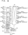
- Fig.20 shows an illustrative structure of the example 8.
- the present example illustrates the structure of an optical switch for four transmission channels and four reception channels practicing the eighteenth aspect of the present invention.
- an optical switch of the present example includes four variable wavelength electrical/optical converters (E/O) 860, four address decoders 861, four fixed wavelength filters 862, four optical/electrical converters 863, a light combining/splitting unit 864 and an address conversion circuit 865.
- E/O variable wavelength electrical/optical converters
- the fixed wavelength filters 862-1 to -4 are optical filters ⁇ 1, ⁇ 2, ⁇ 3 and ⁇ 4 fixedly allocated to the filters 862-1 to -4.
- the variable wavelength electrical/optical converters 860 are electrical/optical converters combined from the variable wavelength semi conductor laser and an electrical field absorbing type semiconductor light modulator and operates responsive to a control signal to convert the input electrical signals to an optical signal of an optional wavelength selected from ⁇ 1, ⁇ 2, ⁇ 3 and ⁇ 4.
- the transmission light wavelength of the variable wavelength electrical/optical converter 860 is controlled by the address information decoded by the address decoder 861.
- variable wavelength electrical/optical converters 860 sets the transmission light wavelength to ⁇ 1 which is equal to the transmission wavelength ⁇ 1 of the fixed wavelength filter connected to the output unit 1 to send the optical signal. That is, the address decoder 861 decodes the address of the output unit which is to be the address in the input unit in order to control the variable wavelength electrical/optical converters 860.
- the optical signals sent from all of the variable wavelength electrical/optical converters 860 are combined (synthesized) by the light combining/splitting unit 864 and split to all fixed wavelength filters 862.
- the variable wavelength electrical/optical converters 860 need to be set to respective different wavelengths.
- the contention resolution circuit perform contention judgment so that the optical signals are of mutually different wavelengths.
- the resulting connection patterns are encoded (or not encoded) and sent in this state to the optical switch control circuit to control the optical switch as an optical switch control signal.
- connection pattern There are three methods of sending the connection pattern (mode), that is (1) a method of sending the connection pattern as a bit map without encoding, (2) a method of encoding the connection pattern and sending the encoded connection pattern as a sender address to an output unit and (3) a method encoding the connection pattern to send the encoded connection pattern as a destination address for the input unit.
- mode There are three methods of sending the connection pattern (mode), that is (1) a method of sending the connection pattern as a bit map without encoding, (2) a method of encoding the connection pattern and sending the encoded connection pattern as a sender address to an output unit and (3) a method encoding the connection pattern to send the encoded connection pattern as a destination address for the input unit.
- mode There are three methods of sending the connection pattern (mode), that is (1) a method of sending the connection pattern as a bit map without encoding, (2) a method of encoding the connection pattern and sending the encoded connection pattern as a sender address to an output unit and (3) a method en
- the control signal accorded to the address decoder 861 needs to be a destination address for the input unit.
- the optical switch control signal accorded by the contention resolution circuit represents a sender address for the output unit.
- the sender address for the output unit accorded from the contention resolution circuit using the address conversion circuit 865 is converted into a destination address for the input unit, which address is accorded to the address decoder 861.
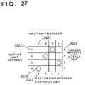
- Fig.26 shows an illustrative structure of a four-channel address conversion circuit made up of four address decoders 891 and four address encoders 892.
- Fig.27 illustrates the operation of the 4-channel address conversion circuit 865 (see Fig.20). Since the address conversion circuit 865 is a circuit used in common by the circuit for converting the sender address for the output unit into a destination address for the input unit and by a circuit for converting the destination address for the input unit into the sender address for the output unit, the operation of converting the sender address for the output unit into a destination address for the input unit is explained as an example.
- Fig.27 shows an example of a connection pattern (mode) interconnecting the input and output units, that is, it shows that input and output units represented by an input unit address 2021 and an output unit address 2022 are interconnected by a connection pattern represented by a bit map pattern 2025. That is, the third input unit and the first output unit are connected together, while the second input unit and the second output unit are connected together. Similarly, the fourth input unit and the third output unit are connected together, while the first input unit and the fourth output unit are connected together.
- the sender addresses for the output units are 3, 2, 4 and 1 for the first, second, third and fourth output units, respectively. If these are entered to the address conversion circuit 865, the address 3 for the output unit 1 is entered at an input line 1009-1.
- the address decoder 891-1 decodes the address entered from the input line 1009-1 to output a signal at a signal line 1022-1 associated with (corresponding to) the address 3.
- the address encoders 892-3 connected to the signal line 1022-1 encodes the address 1 associated with the connection position of the signal line 1022-1 to output the address 1 at the output line 1021-3. Since the output line 1021-3 is associated with the third input unit, the address 1 for the third input unit, that is the destination address for the input unit, is output. Similar conversion is carried out for the remaining input lines 1009-2 to -4. Conversion from the destination addresses for the input unit to the sender address to the output unit occurs in exactly the same manner.
- Fig.21 shows the structure of an Example 9.
- the present example is directed to an optical switch for the four transmission side channels and four reception side channels for practicing the nineteenth aspect of the present application.
- an optical switch of the present example includes four fixed wavelength electrical/optical (E/O) converters 866, four address decoders 868, four wavelength selectors 867, four optical/electrical (O/E) converters 863, a light combining/splitting unit 864 and an address conversion circuit 865.
- E/O electrical/optical
- the fixed wavelength electrical/optical converters 866-1 to -4 are electrical/optical converters, combined from electrical field absorbing type modulator and DFB laser units to which transmission light wavelengths of ⁇ 1, ⁇ 2, ⁇ 3 and ⁇ 4 are allocated fixedly.
- the wavelength selector 867 is an acousto-optical effect optical filter prepared from lithium niobate crystal and can select the wavelength by an external control signal to output optical signals.
- optical signals sent from all fixed wavelength electrical/optical converters 866 are combined by the light combining/splitting unit 864 and split for all avelength selectors 867.
- the wavelength selector 867 is a selective optical filter for selecting an optional one of the plural wavelengths of ⁇ 1, ⁇ 2, ⁇ 3 and ⁇ 4 to transmit the selected wavelength.
- the optical/electrical converters 863 receive only the optical signal transmitted through the wavelength selector 867 for conversion to the electrical signal.
- the transmission light wavelength of the wavelength selector 867 is controlled by the address information decoded by the address decoder 868.
- the transmission light wavelength is set to ⁇ 1 which is the same as the transmission light wavelength ⁇ 1 of the fixed wavelength electrical/optical converter 866-1 of the input unit 1 so that only the optical signal of the wavelength ⁇ 1 is transmitted from the received optical signal and converted by the optical/electrical converters 863-1 into an electrical signal which is received. That is, the output unit decodes the address of the input unit as the sender to control the wavelength selector 867.
- the contention resolution circuit effectuates contention resolution as to which input unit is to transmit in its time slot.
- the resulting connection pattern controls the optical switch as an optical switch control signal.
- the control signal accorded to the address decoder 868 needs to be a sender address for an output unit.
- the optical switch control signal accorded from e.g., the contention resolution circuit may be a destination address for an input unit.
- the sender address for an input unit accorded by e.g., a contention resolution cicuit using the address conversion circuit 865 is converted into a sender address for the output unit, which address is supplied to the address decoder 868.
- Fig.22 shows the structure of the tenth example.
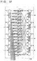
- the present example is directed to an optical switch for four transmission side channels and four reception side channels representing application of the twenty-first aspect to the twentieth aspect of the present application.
- the present example includes four variable wavelength electrical/optical (E/O) converters 871, four address decoders 872, four optical splitters 873, eight optical gates 874, four optical combiners 875, two optical combining/splitting units 876, four fixed wavelength filters 877, four optical combining/splitting units 878 and an address conversion circuit 865.
- E/O electrical/optical
- the fixed wavelength filters 877-1 to -4 are optical filters for transmitting the fixedly allocated wavelengths ⁇ 1, ⁇ 2, ⁇ 3 and ⁇ 4.
- the variable wavelength electrical/optical converters 871 are electrical/optical converters combined from the variable wavelength semiconductor laser and the electrical field absorbing type semiconductor light modulator and are responsive to the control signal to convert the input electrical signals into optical signals of an optional one of the wavelengths ⁇ 1 and ⁇ 2 to output the resulting signals.
- the transmission light wavelength of the variable wavelength electrical/optical converters 871 and the opening/closure of the optical gate 874 are controlled by the address information decoded by the address decoder 872.
- Fig.28 illustrates the control operation of the optical gate 874 and the variable wavelength electrical/optical converters 871 by the address decoder 872.
- the address signal of Fig.28 is a binary representation of the address signal associated with the number at 2026 of the output unit which is the destination of packet. Higher bits 2027 and lower bits 2028 of the address signal in the binary representation are used for controlling the optical gate 874 and the variable wavelength electrical/optical converters 871, respectively. If the higher bits 2027 are 0, the optical gates 874-1, -3, -5 and -7 are turned on, while the optical gates 874-2, -4, -6 and -8 are turned off.
- the variable wavelength electrical/optical converters 871 set the transmission light wavelength to 1 and to 2, respectively.
- an address signal 10 is entered to the address decoder 872-1. Since the lower bit is 0, the transmission light wavelength of the variable wavelength electrical/optical converter 871-1 is set to ⁇ 1 to output a packet light signal. The packet light signal is then branched in the optical splitter 873-1 to enter the optical gates 874-1 and -2. Since the higher bit of the address signal is 1, the optical gate 874-1 is turned off, while the optical gate 874-2 is turned on, so that the packet light signal enters the optical combining/splitter unit 876-2 from the optical combining 875-2 and branched to enter the fixed wavelength filters 877-3 and -4.
- the packet light signal with the transmission light wavelength ⁇ 1 is not transmitted through the fixed wavelength filter 877-4 but is transmitted through the fixed wavelength filter 877-3 so that only the optical/electrical converter 878-3 receives the packet light signal to exchange the packet to the output unit 3.
- the address decoder 872 decodes the address of the output unit of the destination in order to control the variable wavelength electrical/optical converter 871 and the optical gate 874.
- the contention resolution circuit performs contention judgment in order to judge which input unit should transmit in its time slot.
- the connection pattern thus obtained is sent to the optical switch control circuit to control the optical switch as the optical switch control signal.
- the control signal accorded to the address decoder 872 needs to be a destination addresses directed to the input unit.
- the optical switch control signal accorded from the contention resolution circuit might be a sender address directed to the output unit.
- the sender address directed to the output unit accorded from the contention resolution circuit or the like using the address conversion circuit 865 is converted into a destination address for the input unit which is then accorded to the address decoder 872.
- Fig.23 shows the structure of the Example 11.
- the present Example is directed to an optical switch for four transmission side channels and four reception side channels representing an application of the twenty-third aspect to the twenty-second aspect of the invention.
- the present Example includes four fixed wavelength electrical/optical (E/O) converters 881, two optical combining/-splitting units 882, four optical splitters 883, eight light gates 884, four optical combiners 885, four address decoders 886, four wavelength selectors 887, four optical/electrical converters 888 and an address converter circuit 865.
- E/O electrical/optical
- the fixed wavelength electrical/optical converters 881-1 to -4 are electrical/optical converters combined from the electrical field absorbing type modulators and DFB laser units to which are fixedly allocated the transmission light wavelengths of ⁇ 1, ⁇ 2, ⁇ 1, ⁇ 2, respectively.
- the wavelength selector 867 are acousto-optical effect optical filters produced using lithium niobate crystals and can output optical signals by selecting the wavelength by external control signal.
- optical signals transmitted from the fixed wavelength electrical/optical converters 881 of the input units 1 and 2 are combined by the optical combining/splitting units 882 and split to optical splitters 883-1 and -3 and thence sent to the optical gates 884-1, 884-3, 884-5 and 884-7.
- the address decoder 886-1 controls two optical gates 884-1 and 884-2, one 884-1 of which is turned on to send the signal of the input unit 1 or 2 through the optical combiner 885-1 to the wavelength selector 887-1 which then selects the transmission light wavelength ⁇ 1 or ⁇ 2 to select and transmit the optical signal of the input unit 1 or the optical signal of the input unit 2 for reception by the optical/electrical converter 888-1.
- the control signal of the address decoder 886-1 turns the optical gate 884-1 on in order to set the connection to the input unit to be connected to the output unit 1. This selects the input units 1 and 2 of the input units 1 to 4. On the other hand, the selected transmission light wavelength of the wavelength selector 887-1 is controlled to ⁇ 1 to select the input unit 1. That is, the address decoder 886-1 acquires the transmitter (sender) address for the output unit 1 to decode the address to control the optical gate and the wavelength selector, and hence the optical switch.
- the contention resolution circuit judges contention as to which input unit transmits the packet in its time slot.
- the connection pattern obtained in this manner is sent to the optical switch control circuit to control the optical switch as an optical switch control signal.
- the control signal accorded to the address decoder 868 needs to be a destination address for an input unit.
- the optical switch control signal is the sender address for the output unit.
- the sender address for an output unit accorded by e.g., a contention resolution circuit etc. using the address conversion circuit 865 is converted into a destination address for the input unit, which address is accorded to the address decoder 886.
- Fig.29 shows the structure of the twelfth example.
- the present example is directed to an optical packet exchange apparatus for four transmission side channels and four reception side channels representing application of the third aspect to the first aspect of the present application.
- the present example includes four input units 901, a sole optical switch 100, four output units 902, a contention resolution circuit 103 and a sole optical switch control circuit 104.
- the input unit 101 and the output unit 102 of the optical packet exchange apparatus of the first embodiment are respectively changed to the input unit 901 shown in Fig.30 and to the output unit 902 shown in Fig.31.
- the following description of the present Example is mainly directed to the input unit 901 and the output unit 902.
- Fig.30 shows an illustrative structure of the sole input unit 901 of the present Example.
- the input unit 901 includes a destination addresses extraction circuit 105, an input packet buffer 107, an address buffer 109, a packet readout circuit 110, an encoding circuit 950, a parallel/serial converter 111 and an electro-optical (E/O) converter 112.
- the destination address extraction circuit 105 extracts the destination address of the input packet signal 1001 to buffer the address in the address buffer 109 while buffering the packet in the input packet buffer 107.
- the address buffer 109 outputs a destination address signal 1003 and a connection request signal 1004 to the contention resolution circuit.
- the packet readout circuit 110 on reception of the connection permission signal 1005 from the contention resolution circuit erases the associated address in the address buffer 109 to take out an associated packet from the input packet buffer 107 to output it to the encoding circuit 950.
- the encoding circuit 950 in the present example is an 8B/10B encoding circuit for doing 8B/10B encoding.
- 8B/10B encoding converts an 8-bit signal into a 10-bit signal and, in the as-converted pattern, the number of the same bit appearing consecutively is not more than 5 and the mark ratio of 1/2 is assured by running disparity.
- the running disparity means such a signal which is plus or minus if the number of 1 in data transmitted so far is larger or smaller than the number of 0 .
- the two sorts of 10-bit signals are allocated for the same 8-bit input signal. If the number 0 is larger in one of the codes, the number 1 is set so as to be larger in the other code, so that, if the running disparity is plus or minus, the code with a larger number of 0 and the code with a larger number of 1 is used for encoding, respectively, with the mark ratio being 1/2.
- the output is suppressed to not exceeding five consecutive bits of the same code, with the mark ratio being 1/2. For example, if all of 8 bits entering the 8B/10B encoding circuit are "0", that is if "00000000" is entered, an output is 1001110100 or 0110001011 depending on the running disparity being minus or plus, respectively.
- the encoding circuit 950 continues to output a dummy packet pattern for which there can occur no malfunction of the electrical/optical converter 112, with the parallel/serial converter 111 converting the packet signal from a parallel signal to a serial signal and with the electrical/optical converter 112 converting the serial signal into an optical signal 1002.
- This optical signal 1002 is output to the optical switch 100.
- FIG.31 shows an illustrative structure of the output unit 902 in the present example.
- the output unit 902 is made up of an optical/electrical (O/E) converter 113, a serial/parallel (S/P) converter 114, a decoding circuit 951 and a packet eliminating circuit (eliminator) 115.
- An optical signal 1006 entered from the optical switch 100 is converted by the optical/electrical converter 113 into the electrical signal which is then converted into parallel signals by the serial/parallel converter 114 so as to be sent to the decoding circuit 951 for decoding.
- the decoded packet is entered to the packet eliminating circuit 115. If the packet discarding signal 1008 is supplied from the contention resolution circuit, the packet is discarded, such that the output packet signal 1007 is devoid of packets.
- the received packet signal is output as the output packet signal 1007. If there is no packet to be received in the output unit 902, a dummy packet pattern or a packet addressed to another output unit is entered. However, since the packet discarding signal 1008 is sent from the contention resolution circuit, there is no risk of a packet addressed to an incorrect output unit being erroneously transferred to a receiving station.
- Fig.32 shows the structure of the Example 13.
- the present Example is directed to an optical packet exchange apparatus for four transmission channels and four reception channels representing application of the seventh and eighth aspects to the fifth aspect of the present invention.
- the optical packet exchange apparatus of the present Example is made up of four input units 901, an optical switch 100, four output units 903, a contention resolution circuit 103 and an optical switch control circuit 104 and corresponds to the optical packet exchange apparatus of Example 12 in which the output unit 902 is changed to the output unit 903 shown in Fig.33.
- the following description is directed mainly to the operation of the output unit 903 in the present Example.
- Fig.33 shows an illustrative structure of the output unit 903 of the present Example.
- the output unit 903 is made up of an optical/electrical (O/E) converter 313, a serial/parallel (S/P) converter 314, a decoding circuit 951, a packet eliminating circuit 315 and an address comparator circuit 324.
- the optical signal 1006, entered from the optical switch is converted by the optical/electrical converter 313 into an electrical signal which is converted into parallel signals by the serial/parallel converter 314.
- the parallel signals are decoded by the decoding circuit 951 so as to be sent to the packet eliminating circuit 315 and to the address comparator circuit 324.
- the address comparator circuit 324 extracts the destination address information of the packet header to compare it with the address of the own output unit. If the packet destination address coincides with the own address, the address comparator circuit 324 commands the packet to pass through it. Otherwise, the address comparator circuit 324 commands the packet eliminating circuit 315 to discard the packet.
- the output unit 903 If the output unit 903 is fed with a dummy packet pattern encoded corresponding to an all "0" packet, it is decoded by the decoding circuit 951 to an all "0" packet. Thus, there is no packet output to the receiving station even if it is not eliminated by the packet eliminating circuit 315. If a packet addressed to a different output unit is received, it is detected by the address comparator circuit 324 after decoding by the decoding circuit 951 so as to be discarded by the packet eliminating circuit 315. Thus, there is no risk of the packet addressed to a different output unit being erroneously transferred to the receiving station.
- Fig.34 shows the structure of the Example 14.
- the present Example is directed to an optical packet exchange apparatus for four transmission channels and four reception channels representing application of the thirteenth aspect to the eleventh aspect of the present invention.
- the optical packet exchange apparatus of the present Example is made up of four input units 901, an optical switch 100, four output units 904, a contention resolution circuit 503, a dummy packet destination address calculating circuit 525, and an optical switch control circuit 104.
- the present example corresponds to the optical packet exchange apparatus of Example 5 in which the input unit 101 is changed to the input unit 901 of the Example 12, and the output unit 502 is changed to an output unit 904 shown in Fig.35.
- the following description is centered on the operation of the output unit 904 in the present Example.
- Fig.35 shows an illustrative structure of the output unit 904 of the present Example.
- the output unit 904 is made up of an optical/electrical converter 513, a serial/parallel converter 514 and a decoding circuit 951.
- the optical signal 1006, entered from the optical switch, is converted by the optical/electrical converter 113 into an electrical signal which is converted into parallel signals by the serial/parallel converter 114.
- the parallel signals are decoded by the decoding circuit 951.
- a dummy packet pattern corresponding to the encoded all "0" packet, is entered to the output unit 904, it is decoded by the decoding circuit 951 to an all "0"-packet, so that there is no risk of an erroneous packet being output to the receiving station, thus enabling a regular exchange operation.
- Fig.36 shows the structure of the Example 15.
- the present Example is directed to an optical packet exchange apparatus for four transmission channels and four reception channels representing application of the sixteenth aspect to the fourteenth aspect of the present invention.
- the optical packet exchange apparatus of the present Example is made up of four input units 901, an optical switch 100, four output units 904, a contention resolution circuit 603, a dummy packet sender address calculating circuit 625 and an optical switch control circuit 104, and corresponds to the optical packet exchange apparatus of Example 6 in which the input unit 101 is changed to an input unit 901 of Example 12 and the output unit 502 is changed to the output unit 904 shown in Fig.35.
- the output unit 904 devoid of the packet to be received can be connected by an extremely simplified step to the input unit 901 devoid of the packet to be transmitted, as explained in connection with the Example 6.
- a dummy packet pattern corresponding to the encoded all "0"-packet is output from the input unit 901 devoid of the packet to be transmitted, as explained in connection with the Example 12.
- the dummy packet pattern is received by the output unit 904 connected to the input unit 901 so that the optical/electrical converter 513 can operate without errors. Since the received dummy packet pattern is decoded by the decoding circuit 951 into an all "0"-packet, there is no risk of an incorrect packet being output to the receiving station to enable a regular exchange operation.
- the optical/electrical converter which is inexpensive and fast in operation, can be controlled speedily without the risk of erroneous operation.
- Examples 1 to 7 and 12 to 15 are packet exchange apparatus having four transmission side channels and four reception side channels, the numbers of channels can be optionally selected on the transmission and reception sides.
- the optical switch 100 is a splitter/combiner type optical switch having four optical splitters, 16 optical gates 11 and four optical combiners 12.
- the structure of the optical switch in the first to seventeenth aspects of the present invention is, however, not limited to the splitter/combiner type and may be of any suitable structure provided that optical signals entered from different input ports can be output from the same output port.
- encoding circuits and decoding circuits may also be provided on the input and output units, respectively.
- the dummy packet generating circuit 106 is provided independently of the input packet buffer 107, and the selector 108 is controlled by a packet readout circuit.
- a dummy packet pattern storage area may be provided in the input packet buffer 107 so that a dummy packet may be read out from this storage are a for transmission under control by the dummy packet readout circuit 110.
- the optical switch is of the four transmission side channels and four reception side channels.
- the number of channels may be freely selected for both the transmission and reception sides.
- a semiconductor light amplifier is used.
- other devices may be used as the optical gate.
- the devices that may be used include an electrical field absorbing type optical modulator, an optical switch mounted on a lithium niobate substrate and which utilizes an electro-optical or acousto-optical effect, an optical switch formed of a polymer waveguide, a liquid crystal optical switch, a mechanical optical switch and an optical fiber amplifier etc.
- a combination of a variable wavelength semi conductor laser light source and an electrical field absorbing type semiconductor optical modulator is used as the variable wavelength electrical/optical converter.
- a tunable DFB laser, a tunable DBR laser or a tunable external resonator type laser may also be used as a light source.
- the electrical field absorbing type modulator is used as a modulator, the material and the structure of the optical modulator may be selected otherwise.
- the optical modulator exploiting the electro-optical effect or the acousto-optical effect proper to the lithium niobate crystal may also be used.
- an acousto-optical effect optical filter formed by a lithium niobate crystal is used as a wavelength selector.
- the wavelength selector in the nineteenth, twenty-second and twenty-third aspects of the present invention may be of any suitable structure provided that it can select and output one of plural wavelengths.
- the wavelength filter or selector comprised of the optical length splitter, optical gate and an optical combining device or a mechanical variable wavelength filter may be used.
- optical packet exchange apparatus and optical switch According to the present invention, if, in an optical packet exchange apparatus, there is no packet to be transmitted, and a dummy packet is sent so that there is no "0" or "1" bit pattern continuing for a longer time than a pre-set period to prevent malfunction of the optical/electrical converter of the output unit, search for a connection pattern between an input unit devoid of a packet for transmission and an output unit devoid of a packet for reception is reduced and can be effected speedily, so that fast switch control can be realized even if the number of channels of the exchange apparatus or the network speed is increased.
- the hardware quantity (or volume) may also be reduced.
- dummy packets or packets used in substitution of dummy packets and which are addressed to different receiving stations can be eliminated speedily to prevent malfunction of the reception station without lowering the operating speed of the packet exchange apparatus.
- the optical gate and the wavelength selector in an optical switch can be controlled by the same address decoder, the number of control lines can be decreased, while broadcasting or multi casting is facilitated. Since there is no congestion of the optical wiring between the optical gates and the wavelength selectors, synchronous control of the optical gates and the wavelength selectors is also facilitated.
Landscapes
- Engineering & Computer Science (AREA)
- Computer Networks & Wireless Communication (AREA)
- Signal Processing (AREA)
- Data Exchanges In Wide-Area Networks (AREA)
- Optical Communication System (AREA)
- Use Of Switch Circuits For Exchanges And Methods Of Control Of Multiplex Exchanges (AREA)
Applications Claiming Priority (2)
| Application Number | Priority Date | Filing Date | Title |
|---|---|---|---|
| JP36286097 | 1997-12-12 | ||
| JP36286097A JP3164049B2 (ja) | 1997-12-12 | 1997-12-12 | 光パケット交換装置 |
Publications (3)
| Publication Number | Publication Date |
|---|---|
| EP0923263A2 true EP0923263A2 (fr) | 1999-06-16 |
| EP0923263A3 EP0923263A3 (fr) | 2007-01-03 |
| EP0923263B1 EP0923263B1 (fr) | 2008-12-10 |
Family
ID=18477918
Family Applications (1)
| Application Number | Title | Priority Date | Filing Date |
|---|---|---|---|
| EP98123440A Expired - Lifetime EP0923263B1 (fr) | 1997-12-12 | 1998-12-11 | Système de commutation de paquets optiques et commutateur optique |
Country Status (4)
| Country | Link |
|---|---|
| US (3) | US6441935B1 (fr) |
| EP (1) | EP0923263B1 (fr) |
| JP (1) | JP3164049B2 (fr) |
| DE (1) | DE69840318D1 (fr) |
Cited By (1)
| Publication number | Priority date | Publication date | Assignee | Title |
|---|---|---|---|---|
| EP1755241A4 (fr) * | 2004-06-10 | 2012-08-01 | Fujikura Ltd | Appareil de communication optique et systeme de communication optique |
Families Citing this family (43)
| Publication number | Priority date | Publication date | Assignee | Title |
|---|---|---|---|---|
| JP2000078675A (ja) * | 1998-09-02 | 2000-03-14 | Fujitsu Ltd | Dma通信及びsd/scn信号による交換機内部装置制御システム |
| JP3440886B2 (ja) * | 1999-06-16 | 2003-08-25 | 日本電気株式会社 | 波長多重光伝送システム |
| JP3374174B2 (ja) * | 1999-12-15 | 2003-02-04 | 独立行政法人通信総合研究所 | フォトニックネットワークのパケットルーティング方法およびフォトニックネットワーク用パケットルータ |
| US6661976B1 (en) * | 2000-01-05 | 2003-12-09 | At&T Corp. | Method and system for single-sideband optical signal generation and transmission |
| JP3646638B2 (ja) | 2000-09-06 | 2005-05-11 | 日本電気株式会社 | パケット交換装置及びそれに用いるスイッチ制御方法 |
| JPWO2002063890A1 (ja) * | 2001-02-07 | 2004-06-10 | 富士通株式会社 | クロスコネクト装置 |
| US20020122225A1 (en) * | 2001-03-01 | 2002-09-05 | Yigal Rappaport | Multiport wavelength division multiplex network element |
| US20020154361A1 (en) * | 2001-04-20 | 2002-10-24 | Benny Pesach | Wavelength division multiplexed (WDM) network element and a method for propagating data packets across the network element |
| WO2002093389A1 (fr) * | 2001-05-17 | 2002-11-21 | Decru, Inc. | Interconnexion a flux oriente permettant un stockage informatique en reseau |
| KR100420949B1 (ko) * | 2001-08-14 | 2004-03-02 | 한국전자통신연구원 | 광 스위칭 방법 및 그 장치 |
| JP3851836B2 (ja) | 2002-04-19 | 2006-11-29 | 富士通株式会社 | 波長多重伝送システム及び波長多重伝送装置 |
| JP4039192B2 (ja) * | 2002-09-20 | 2008-01-30 | 富士ゼロックス株式会社 | 光伝送装置 |
| ATE318028T1 (de) * | 2003-10-09 | 2006-03-15 | Cit Alcatel | Optische paketübertragung |
| US7848644B2 (en) | 2004-02-23 | 2010-12-07 | Dynamic Method Enterprises Limited | Method and an apparatus to provide optical equipment protection |
| JP4495484B2 (ja) * | 2004-02-24 | 2010-07-07 | 富士通マイクロエレクトロニクス株式会社 | 描画データ生成装置 |
| JP4382635B2 (ja) | 2004-11-10 | 2009-12-16 | 富士通株式会社 | 光伝送装置 |
| JP4291281B2 (ja) * | 2005-02-03 | 2009-07-08 | 富士通株式会社 | 情報処理システム、計算ノード、情報処理システムの制御方法 |
| JP4564389B2 (ja) * | 2005-03-31 | 2010-10-20 | Kddi株式会社 | 光ルーティング装置および光ルーティング方法 |
| US7965708B2 (en) * | 2005-06-07 | 2011-06-21 | Cisco Technology, Inc. | Method and apparatus for using meta-packets in a packet processing system |
| JP4527650B2 (ja) * | 2005-10-31 | 2010-08-18 | 富士通株式会社 | 物理配線制御装置、物理配線制御方法および物理配線制御プログラム |
| WO2007056713A2 (fr) * | 2005-11-04 | 2007-05-18 | The Trustees Of Columbia University In The City Of New York | Reseau optique |
| US7881617B2 (en) * | 2006-02-24 | 2011-02-01 | Cisco Technology, Inc. | Buffering schemes for optical packet processing |
| US7835649B2 (en) | 2006-02-24 | 2010-11-16 | Cisco Technology, Inc. | Optical data synchronization scheme |
| JP4675812B2 (ja) * | 2006-03-30 | 2011-04-27 | 株式会社東芝 | 磁気記録媒体、磁気記録装置および磁気記録媒体の製造方法 |
| US8582972B2 (en) * | 2006-08-31 | 2013-11-12 | The Trustees Of Columbia University In The City Of New York | Systems and methods for storing optical data |
| JP4376263B2 (ja) * | 2006-12-08 | 2009-12-02 | 富士通株式会社 | 光波長多重システム |
| WO2008080122A2 (fr) | 2006-12-22 | 2008-07-03 | The Trustees Of Columbia University In The City Of New York | Systèmes et procédé pour une communication de données intégrées |
| WO2009015691A1 (fr) * | 2007-07-31 | 2009-02-05 | Telefonaktiebolaget Lm Ericsson (Publ) | Contrôleur de commutation optique |
| US20100205060A1 (en) * | 2009-02-09 | 2010-08-12 | Yahoo! Inc. | Context-sensitive route generation system |
| US8467682B2 (en) * | 2010-10-29 | 2013-06-18 | Lockheed Martin Corporation | Reliable load-balanced multi-photonic star configuration |
| JP5545753B2 (ja) * | 2010-12-20 | 2014-07-09 | 富士通テレコムネットワークス株式会社 | 光パケット交換システム |
| JP5588374B2 (ja) * | 2011-02-08 | 2014-09-10 | 富士通テレコムネットワークス株式会社 | 光パケット交換システム、光パケット交換装置、および光パケット送信装置 |
| JP2012165267A (ja) * | 2011-02-08 | 2012-08-30 | Fujitsu Telecom Networks Ltd | 光パケット交換システムおよび光パケット交換装置 |
| JP5439408B2 (ja) * | 2011-02-09 | 2014-03-12 | 富士通テレコムネットワークス株式会社 | 光パケット交換システムおよび光パケット送信装置 |
| JP5426604B2 (ja) * | 2011-04-26 | 2014-02-26 | 富士通テレコムネットワークス株式会社 | 光パケット交換システム |
| US9628878B2 (en) | 2012-12-11 | 2017-04-18 | Huawei Technologies Co., Ltd. | System and method for multi-wavelength encoding |
| US9959424B2 (en) * | 2014-03-12 | 2018-05-01 | Michael Bilotta | Information based life view |
| US20190188230A1 (en) | 2014-03-12 | 2019-06-20 | Michael Bilotta | Systems and methods for an information-based life view |
| US9712899B2 (en) * | 2014-12-11 | 2017-07-18 | Alcatel Lucent | Hybrid optical switch for software-defined networking |
| US10218453B2 (en) * | 2016-04-27 | 2019-02-26 | Juniper Networks, Inc. | Methods and apparatus for logical associations between routers and optical nodes within a wavelength division multiplexing (WDM) system |
| US10015568B2 (en) * | 2016-10-11 | 2018-07-03 | Fluke Corporation | Optically-addressable optical switch |
| JP7618998B2 (ja) * | 2020-10-13 | 2025-01-22 | 日本電気株式会社 | 演算処理装置、方法及びプログラム |
| WO2024038540A1 (fr) * | 2022-08-18 | 2024-02-22 | Nippon Telegraph And Telephone Corporation | Système de commutation, appareil de transmission de paquet optique et procédé de génération de paquet optique |
Family Cites Families (22)
| Publication number | Priority date | Publication date | Assignee | Title |
|---|---|---|---|---|
| US4834483A (en) * | 1987-05-06 | 1989-05-30 | Bell Communications Research, Inc. | Fast optical cross-connect for parallel processing computers |
| US4873681A (en) * | 1988-01-26 | 1989-10-10 | Bell Communications Research, Inc. | Hybrid optical and electronic packet switch |
| JPH025663A (ja) * | 1988-06-23 | 1990-01-10 | Nec Corp | 光パケット交換装置 |
| US5005167A (en) * | 1989-02-03 | 1991-04-02 | Bell Communications Research, Inc. | Multicast packet switching method |
| JP2781633B2 (ja) * | 1990-01-10 | 1998-07-30 | 株式会社日立製作所 | セル信号処理回路及びそれを用いた光交換機 |
| JPH0410722A (ja) * | 1990-04-27 | 1992-01-14 | Hitachi Ltd | コヒーレント通信方法、クロスコネクト装置及び交換装置 |
| JPH0472939A (ja) | 1990-07-13 | 1992-03-06 | Hitachi Ltd | 光スイッチを用いたパケット交換装置 |
| JPH04162852A (ja) | 1990-10-26 | 1992-06-08 | Hitachi Ltd | 光スイッチを用いたパケット交換装置 |
| US5093743A (en) * | 1990-12-28 | 1992-03-03 | At&T Bell Laboratories | Optical packet switch |
| FR2683962B1 (fr) * | 1991-11-19 | 1994-03-25 | Lecoquil Emile | Repartiteur optique. |
| FR2690801B1 (fr) * | 1992-04-29 | 1994-10-28 | France Telecom | Multiplexeur à insertion et extraction. |
| ES2145846T3 (es) * | 1993-11-08 | 2000-07-16 | British Telecomm | Sistema de interconexion para una red optica. |
| CA2185138C (fr) * | 1994-03-29 | 2001-01-23 | Alan Michael Hill | Reseau optique de telecommunications |
| FR2729040B1 (fr) * | 1994-12-29 | 1997-01-31 | Alcatel Nv | Matrice de commutation photonique |
| US5627925A (en) * | 1995-04-07 | 1997-05-06 | Lucent Technologies Inc. | Non-blocking optical cross-connect structure for telecommunications network |
| JPH0998188A (ja) | 1995-07-27 | 1997-04-08 | Canon Inc | 信号交換方法及びそれを用いる信号交換装置及びそれを用いるネットワークシステム |
| US5724167A (en) * | 1995-11-14 | 1998-03-03 | Telefonaktiebolaget Lm Ericsson | Modular optical cross-connect architecture with optical wavelength switching |
| JP3459737B2 (ja) | 1995-12-14 | 2003-10-27 | キヤノン株式会社 | ネットワークシステム、そこで用いられる交換装置における通信方法 |
| JP2718407B2 (ja) | 1995-12-15 | 1998-02-25 | 日本電気株式会社 | 光スイッチ装置及び光スイッチ制御方法 |
| GB2316573B (en) * | 1996-08-14 | 2001-04-18 | Fujitsu Ltd | Switching apparatus |
| JP3036589B2 (ja) | 1997-02-26 | 2000-04-24 | 日本電気株式会社 | 光ネットワーク制御方式および光ネットワーク |
| FR2784468B1 (fr) * | 1998-10-08 | 2000-12-15 | Cit Alcatel | Matrice de commutation atm comportant un noyau optique passif |
-
1997
- 1997-12-12 JP JP36286097A patent/JP3164049B2/ja not_active Expired - Fee Related
-
1998
- 1998-12-11 EP EP98123440A patent/EP0923263B1/fr not_active Expired - Lifetime
- 1998-12-11 US US09/210,277 patent/US6441935B1/en not_active Expired - Fee Related
- 1998-12-11 DE DE69840318T patent/DE69840318D1/de not_active Expired - Lifetime
-
2002
- 2002-04-16 US US10/123,444 patent/US6570687B2/en not_active Expired - Fee Related
- 2002-05-21 US US10/151,789 patent/US6957018B2/en not_active Expired - Fee Related
Cited By (1)
| Publication number | Priority date | Publication date | Assignee | Title |
|---|---|---|---|---|
| EP1755241A4 (fr) * | 2004-06-10 | 2012-08-01 | Fujikura Ltd | Appareil de communication optique et systeme de communication optique |
Also Published As
| Publication number | Publication date |
|---|---|
| DE69840318D1 (de) | 2009-01-22 |
| US6570687B2 (en) | 2003-05-27 |
| JP3164049B2 (ja) | 2001-05-08 |
| US6441935B1 (en) | 2002-08-27 |
| EP0923263B1 (fr) | 2008-12-10 |
| EP0923263A3 (fr) | 2007-01-03 |
| US6957018B2 (en) | 2005-10-18 |
| JPH11177624A (ja) | 1999-07-02 |
| US20020131120A1 (en) | 2002-09-19 |
| US20020109882A1 (en) | 2002-08-15 |
Similar Documents
| Publication | Publication Date | Title |
|---|---|---|
| EP0923263B1 (fr) | Système de commutation de paquets optiques et commutateur optique | |
| US5377182A (en) | Non-blocking crossbar permutation engine with constant routing latency | |
| US5617233A (en) | Transparent optical node structure | |
| AU706670B2 (en) | A network system having transmission control for plural node devices without arbitration, and transmission control method therefore | |
| JP2004193817A (ja) | スキュー調整方式 | |
| US5742585A (en) | Network for connecting a plurality of nodes using a plurality of channels | |
| US10687130B2 (en) | Intelligence-defined optical tunnel network system controller and control method thereof | |
| US5786917A (en) | Optical switching network and control method for same | |
| EP0755138B1 (fr) | Dispositif de noeud d'un réseau | |
| JP3335087B2 (ja) | ネットワークシステム及びノード装置及びその制御方法 | |
| US6317429B1 (en) | Communication apparatus, network system using communication apparatus and control method used in network system | |
| CN101931488B (zh) | 全时全通型量子网络路由器及扩展量子保密通信网络的方法 | |
| JPH09289520A (ja) | 伝送制御方法及びそれを用いたネットワークシステム | |
| EP1665867B1 (fr) | Noeud pour reseau de communication optique | |
| JP3279259B2 (ja) | 並列伝送方法及びシステム | |
| JP3534473B2 (ja) | 光バッファメモリ | |
| JP3459737B2 (ja) | ネットワークシステム、そこで用いられる交換装置における通信方法 | |
| JPH01229545A (ja) | 光パケットスイッチ | |
| JP3687844B2 (ja) | 光パケットネットワーク | |
| JP2874540B2 (ja) | 光atmスイッチ | |
| JPH0729390A (ja) | 光バッファメモリ | |
| JP3371996B2 (ja) | 光伝送装置および光ネットワーク | |
| JP2005117603A (ja) | 光通信方式 | |
| AU768042B2 (en) | Multiple level minimum logic network | |
| JPH04213941A (ja) | 光通信方法 |
Legal Events
| Date | Code | Title | Description |
|---|---|---|---|
| PUAI | Public reference made under article 153(3) epc to a published international application that has entered the european phase |
Free format text: ORIGINAL CODE: 0009012 |
|
| AK | Designated contracting states |
Kind code of ref document: A2 Designated state(s): AT BE CH CY DE DK ES FI FR GB GR IE IT LI LU MC NL PT SE |
|
| AX | Request for extension of the european patent |
Free format text: AL;LT;LV;MK;RO;SI |
|
| RIC1 | Information provided on ipc code assigned before grant |
Ipc: H04L 12/56 20060101ALI20060907BHEP Ipc: H04Q 11/00 20060101AFI19990320BHEP |
|
| PUAL | Search report despatched |
Free format text: ORIGINAL CODE: 0009013 |
|
| AK | Designated contracting states |
Kind code of ref document: A3 Designated state(s): AT BE CH CY DE DK ES FI FR GB GR IE IT LI LU MC NL PT SE |
|
| AX | Request for extension of the european patent |
Extension state: AL LT LV MK RO SI |
|
| 17P | Request for examination filed |
Effective date: 20061213 |
|
| 17Q | First examination report despatched |
Effective date: 20070208 |
|
| 17Q | First examination report despatched |
Effective date: 20070208 |
|
| AKX | Designation fees paid |
Designated state(s): DE FR GB |
|
| GRAP | Despatch of communication of intention to grant a patent |
Free format text: ORIGINAL CODE: EPIDOSNIGR1 |
|
| GRAS | Grant fee paid |
Free format text: ORIGINAL CODE: EPIDOSNIGR3 |
|
| GRAA | (expected) grant |
Free format text: ORIGINAL CODE: 0009210 |
|
| AK | Designated contracting states |
Kind code of ref document: B1 Designated state(s): DE FR GB |
|
| REG | Reference to a national code |
Ref country code: GB Ref legal event code: FG4D |
|
| REF | Corresponds to: |
Ref document number: 69840318 Country of ref document: DE Date of ref document: 20090122 Kind code of ref document: P |
|
| PLBE | No opposition filed within time limit |
Free format text: ORIGINAL CODE: 0009261 |
|
| STAA | Information on the status of an ep patent application or granted ep patent |
Free format text: STATUS: NO OPPOSITION FILED WITHIN TIME LIMIT |
|
| 26N | No opposition filed |
Effective date: 20090911 |
|
| PGFP | Annual fee paid to national office [announced via postgrant information from national office to epo] |
Ref country code: DE Payment date: 20131204 Year of fee payment: 16 Ref country code: GB Payment date: 20131211 Year of fee payment: 16 |
|
| PGFP | Annual fee paid to national office [announced via postgrant information from national office to epo] |
Ref country code: FR Payment date: 20131209 Year of fee payment: 16 |
|
| REG | Reference to a national code |
Ref country code: DE Ref legal event code: R119 Ref document number: 69840318 Country of ref document: DE |
|
| GBPC | Gb: european patent ceased through non-payment of renewal fee |
Effective date: 20141211 |
|
| REG | Reference to a national code |
Ref country code: FR Ref legal event code: ST Effective date: 20150831 |
|
| PG25 | Lapsed in a contracting state [announced via postgrant information from national office to epo] |
Ref country code: GB Free format text: LAPSE BECAUSE OF NON-PAYMENT OF DUE FEES Effective date: 20141211 Ref country code: DE Free format text: LAPSE BECAUSE OF NON-PAYMENT OF DUE FEES Effective date: 20150701 |
|
| PG25 | Lapsed in a contracting state [announced via postgrant information from national office to epo] |
Ref country code: FR Free format text: LAPSE BECAUSE OF NON-PAYMENT OF DUE FEES Effective date: 20141231 |