EP0923811B1 - Utilisation d'un circulateur dans des radios en duplex a repartition dans le temps - Google Patents
Utilisation d'un circulateur dans des radios en duplex a repartition dans le temps Download PDFInfo
- Publication number
- EP0923811B1 EP0923811B1 EP97938071A EP97938071A EP0923811B1 EP 0923811 B1 EP0923811 B1 EP 0923811B1 EP 97938071 A EP97938071 A EP 97938071A EP 97938071 A EP97938071 A EP 97938071A EP 0923811 B1 EP0923811 B1 EP 0923811B1
- Authority
- EP
- European Patent Office
- Prior art keywords
- circulator
- receiver
- transmitter
- port
- transmit
- Prior art date
- Legal status (The legal status is an assumption and is not a legal conclusion. Google has not performed a legal analysis and makes no representation as to the accuracy of the status listed.)
- Expired - Lifetime
Links
- 230000005540 biological transmission Effects 0.000 claims description 24
- 230000008878 coupling Effects 0.000 description 3
- 238000010168 coupling process Methods 0.000 description 3
- 238000005859 coupling reaction Methods 0.000 description 3
- 230000000694 effects Effects 0.000 description 3
- 238000002955 isolation Methods 0.000 description 2
- 238000000034 method Methods 0.000 description 2
- 230000015556 catabolic process Effects 0.000 description 1
- 230000001413 cellular effect Effects 0.000 description 1
- 230000007812 deficiency Effects 0.000 description 1
- 238000006731 degradation reaction Methods 0.000 description 1
- 230000001419 dependent effect Effects 0.000 description 1
- 230000001627 detrimental effect Effects 0.000 description 1
- 238000010586 diagram Methods 0.000 description 1
- 230000035945 sensitivity Effects 0.000 description 1
- 230000003595 spectral effect Effects 0.000 description 1
- 229910000859 α-Fe Inorganic materials 0.000 description 1
Images


Classifications
-
- H—ELECTRICITY
- H04—ELECTRIC COMMUNICATION TECHNIQUE
- H04B—TRANSMISSION
- H04B1/00—Details of transmission systems, not covered by a single one of groups H04B3/00 - H04B13/00; Details of transmission systems not characterised by the medium used for transmission
- H04B1/38—Transceivers, i.e. devices in which transmitter and receiver form a structural unit and in which at least one part is used for functions of transmitting and receiving
- H04B1/40—Circuits
- H04B1/44—Transmit/receive switching
- H04B1/48—Transmit/receive switching in circuits for connecting transmitter and receiver to a common transmission path, e.g. by energy of transmitter
-
- H—ELECTRICITY
- H04—ELECTRIC COMMUNICATION TECHNIQUE
- H04B—TRANSMISSION
- H04B1/00—Details of transmission systems, not covered by a single one of groups H04B3/00 - H04B13/00; Details of transmission systems not characterised by the medium used for transmission
- H04B1/38—Transceivers, i.e. devices in which transmitter and receiver form a structural unit and in which at least one part is used for functions of transmitting and receiving
- H04B1/40—Circuits
- H04B1/54—Circuits using the same frequency for two directions of communication
- H04B1/56—Circuits using the same frequency for two directions of communication with provision for simultaneous communication in two directions
Definitions
- the present invention relates to a radio transmitter/receiver apparatus for transmission and reception of information, and in particular provides a means to couple a transmitter and a receiver to a common antenna in a duplex radio without the need for a duplexing filter, with reduced transmit path loss and with reduced power handling requirements for T/R switch components.
- the present invention relates to a radio transceiver for providing duplex radio communications by alternately transmitting and receiving on a time division basis.
- This system is called time division duplex or TDD.
- TDD time division duplex
- the antenna needs to be connected at any instant to either the transmitter or receiver but not to both simultaneously.
- a transmitter and receiver operate in time division duplex to transmit and receive respectively in different time slots of a time division multiple access (TDMA) frame period.
- TDMA time division multiple access
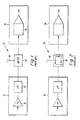
- a known transmitter/receiver or transceiver is illustrated in Figure 1.
- a transceiver 10 includes a transmitter section 12 and a receiver section 14.
- the transmitter section 12 and receiver section 14 are connected to a common antenna 16 by means of a transmit/receive switch 22.
- the transmit/receive switch 22 alternately connects the antenna 16 to either the transmitter section 12 for transmission or the receiver section 14 for reception of signals.
- the transmit/receive switch 22 is controlled by a control means in a known manner which is not illustrated.
- the transmit/receive switch 22 For transmission, the transmit/receive switch 22 connects the antenna 16 to the transmitter section 12, wherein the signals to be transmitted are amplified in a power amplifier 16 and low pass filtered in a filter 20 which removes unwanted harmonics introduced by the power amplifier 18. The filtered signals are then applied to the antenna and transmitted.
- the transmit/receive switch 22 connects the antenna 16 to the receiver section 14 wherein signals that are received by the antenna 16 are sent to the receiver section and are filtered by the receiver filter 24 and are then further processed accordingly to a known manner.
- the transmit/receive switch 22 is usually a diode or MOSFET device. Certain kinds of communications systems must meet transmit spectral component (or side band) intermodulation requirements.
- variable power modulation envelopes such as DAMPS (USA Digital Advanced Mobile Phone Service), PDC (Japan Personal Digital Cellular phone) and other common digital telephone protocols and all other forms of AM and QAM (quadrature phase related amplitude modulation).
- DAMPS USA Digital Advanced Mobile Phone Service
- PDC Pan Personal Digital Cellular phone
- AM and QAM quadrature phase related amplitude modulation
- a further problem of using a simple T/R switch antenna coupling is that power may be reflected back from the antenna to the transmitter which effectively changes the power amplifier load impedance which can degrade the amplifier's own intermodulation characteristics. It is undesirable to combat this effect by increasing the power handling capability of the amplifier, especially in portable equipment, as this reduces power efficiency and thus battery life. High power amplifiers may damage T/R switch components if there is a large amount of reflected power from the antenna.
- FIG. 2 Another way to form a transceiver, is to use a multiport circulator or isolator as illustrated in Figure 2.
- a three port circulator 36 is used to connect a transmit section 32 and a receive section 34 with an antenna 38.
- Figure 2 illustrates the functioning of the circulator 36.
- a B C illustrate connections and in this example, it can be assumed that the circulator has a throughput attenuation of approximately 0.8 dB from the connection A to B, from B to C, and from C to A.
- the reverse isolation is at least 12 dB, i.e., from connection B to A, and A to C, and finally from C to B.
- the circulator allows for signals to be transmitted to pass from the transmitter to the antenna with low attenuation but not to the receiver, (if all transmit power is absorbed by the antenna).
- the circulator antenna duplex connection means any transmit power reflected by the antenna would be conducted to the receiver which must therefore have increased power handling capability for this eventuality. If the transmitter and receiver operated in somewhat different frequency bands, then the receiver input filter 40 would in turn reflect the transmitter power once again to the transmitter, producing the undesirable effects described above. This may happen to a lesser degree even if the frequency is the same due to receiver filter mismatches, which are common.
- signals received at another transmitter's frequency pass to the receiver where they are reflected by the receiver input filter 40since the signals are out-of-band signals.
- Signals reflected from the receiver and back to the circulator will, in the prior art, be passed to the transmitter with low attenuation by the circulator where the reflected signal may appear as an impedance mismatch if the reflection is of the transmitter's own signal or would give rise to so-called back intermodulation if the reflected signal is another transmitter's signal.
- FIG. 3 One way to prevent the reflected signal from being passed to the transmitter is to use a four port circulator as illustrated in Figure 3.
- a transmitter section 52 is connected to a first port of a circulator 54
- an antenna 60 is connected to a second port of the circulator 54
- a receive section 56 is connected to a third port of the circulator 54.
- a load 58 is connected to the fourth port of the circulator 54 wherein signals reflected by the receive section 56 are diverted to the load 58 rather than the transmitter section 52.
- the four port circulator will isolate the transmitter from any antenna reflections but not the receiver. It forms a satisfactory antenna coupling apparatus only if there is no antenna reflection but otherwise reflected transmitter power flows into the receiver where it may overload it.
- JP-A-08 195695 describes a transmitter-receiver with shared antenna, in which a switch is provided between a circulator and the reception side together with a connection of a terminal resistance, in order to reduce the loss of a transmission system, to thereby improve the power efficiency and also to reduce the cost of the components. More specifically, a circulator is connected to an antenna, a transmitter and a receiver, and on the receiver side, a switch is inserted between the circulator and the receiver, where the switch in turn is capable of connecting the circulator to either the receiver or a resistor. When the system is transmitting, the switch is connected to the resistor, such that transmission signals reflected from the antenna and transmitted through the circulator are absorbed by the resistor and not supplied to the receiver.
- the antenna duplexer comprises a high-frequency switching circuit and a band-pass filter.
- the high-frequency switching circuit supplies the transmission signals from a transmission part to the antenna.
- the band-pass filter outputs the reception signals outputted from the antenna to the predetermined receiving circuit.
- the frequency characteristic is selected and set to impress the frequency of the transmission signals, and simultaneously the reflected wave generated at the input end so that the impedance increases at the frequency band of the transmission signals.
- a communications apparatus for a transmitter and receiver for duplex transmission.
- the apparatus comprises a transmit means with a transmit power amplifier, a receiver with a receive filter means, and a circulator with a plurality of ports, wherein said transmit power amplifier is connected to a first port of said circulator and said receiver filter means is connected to a second port of said circulator.
- a transmitter/receiver device is demountably connected to a third port of said circulator and a load means is connected to a fourth port of said circulator.
- a switching means shorts said receiver to ground during transmission so that power reflected by said transmitter/ receiver device is absorbed by said load means.
- a communications apparatus having a transmitter and receiver for duplex transmission.
- the communications apparatus comprises a transmit power amplifier, a receiver filter means, and a circulator with a plurality of ports wherein the transmit power amplifier is connected to a first port and the receiver filter is connected to a second port of the circulator.
- a transmit/receive device is demountably connected to a third port of the circulator.
- An impedance means is located between the circulator and the receive filter wherein the impedance means is a predetermined distance from the receive filter, wherein the impedance means dissipates power reflected by the receive filter means when the transmitter is transmitting.
- the present invention comprises using a switch at a receiver port of a three port circulator operated by a time division duplex control signal alternately to couple a matching impedance to the receive port of the circulator when the transmitter is active in such a way that the signals received or reflected from the antenna during transmission are dissipated in the matching impedance and are thus substantially prevented from reaching the transmitter.
- FIG. 4 illustrates a three port transceiver not belonging to the present invention.
- a three port circulator 70 is used to connect a transmit section 72 and a receive section 74 with an antenna 76.
- the receiver port of the circulator 70 is switched between the receiver section 74 and the load 80 by a transmit/receive switch 78.
- the circulator 70 is connected to the load 80 when the transceiver is transmitting.
- the power level of the signal at the FET, pin diode, or other T/R switch 78 is at least several times less than the power at the antenna.
- the T/R switch 78 need not be of the same size, quality or cost as the switch required in the arrangement disclosed in Figure 1.
- a circulator would be required even if the T/R switch were in the position as in Figure 1 since the reflected power from the antenna would change the transmitter load and thus produce the detrimental effects described above.
- the normal solution is to place the circulator in the transmitter output without otherwise changing the diagram.
- the T/R switch is still connected directly to the antenna and must handle full and reflected power without degradation. This approximately doubles the path loss from the transmitter to the antenna since the power must flow first through the circulator and then through the T/R switch. This shortens the battery life in a portable unit. If the T/R switch is moved to the position as shown, then its attenuation is not added to the transmitter path.
- High level reflected power may still cause distortion in the T/R switch but most of this power will be absorbed by the load.
- An added power detector on the load makes possible a transmitter power reduction at very high antenna mismatches if necessary. This also shrinks the circulator and even the load since it may not need to dissipate much power.
- FIG. 5 illustrates a four port transceiver according to an embodiment of the present invention.
- a four port circulator 90 is used to connect a transmit section 92, a receive section 94, and a load 98 to an antenna 96.
- a switch 100 is closed which shorts the receiver port of the circulator 90 to ground which causes the power reflected by the antenna to be sent to the load 98.
- the switch 100 is open thus allowing the receiver section 94 to receive the signals from the antenna 96.
- the shorting switch 100 may be constructed out of lower cost, lower power consumption and less linear parts than a transmit/receive switch placed directly at the antenna because the shorting switch 100 is not in the power path.
- the switch 100 may be a simple transistor (BJT or FET).
- FIG. 6 illustrates a transceiver according to one embodiment of the present invention.
- a transmitter section 112 and a receiver section 114 are connected to different ports of a three port circulator or isolator 116.
- a transmitter/receiver device such as an antenna 118 is connected to the last port of the circulator 116.
- the inputs and outputs of the transmitter, the receiver, and the antenna are loaded with an impedance of approximately 50 ohms, but the present invention is not limited thereto.
- signals received at another transmitter's frequency or frequencies produced by the transmitter itself may pass to the receiver where they will be reflected by the receiver's input filter 120.
- the reflected signals are not reflected back to the transmitter section 112, but rather are dissipated in a load 122, such as a resistor, which is controlled by a time division duplex control switch 124.
- the switch 124 is controlled by a time division duplex controller (not illustrated) which produces TDD control signals which alternately couples the load 122, to the receive port of the circulator when the transmitter is active in such a way that the signals received or reflected from the antenna during transmission are dissipated in the matching impedance and are thus substantially prevented from reaching the transmitter.
- the load 122 should also have an impedance of approximately 50 ohms.
- the matching impedance In order for the received or reflected signals to be dissipated in the matching impedance, the matching impedance must be a predetermined distance away from the receive filter.
- the predetermined distance can be determined using a Smith Chart.
- the length of the strip line 128 is selected so that the node N1 looks like an opening.
- the receiver In the transmit mode, the receiver is off, thus, the node N1 looks like an opening. If the switch 124 is closed and the antenna is removed, then all of the reflected power will be dumped through the opening into the load 122. Thus, none of the power is reflected back to the power amplifier.
Landscapes
- Engineering & Computer Science (AREA)
- Computer Networks & Wireless Communication (AREA)
- Signal Processing (AREA)
- Transceivers (AREA)
- Transmitters (AREA)
Claims (9)
- Appareil de communication pour un émetteur et un récepteur pour la transmission en duplex, comprenant :un moyen d'émission (92) avec un amplificateur de puissance d'émission;un récepteur (94) avec un filtre de réception;un circulateur (90) avec une pluralité d'accès, dans lequel l'amplificateur de puissance d'émission est connecté à un premier accès du circulateur (90) et le filtre de réception est connecté à un second accès du circulateur (90) ;un dispositif émetteur/récepteur (96) qui est connecté de façon amovible à un troisième accès du circulateur (90) ;une charge (98) connectée à un quatrième accès du circulateur (90); etun moyen de commutation (100) pour court-circuiter le récepteur (94) à la masse pendant l'émission, de façon que la puissance réfléchie par le dispositif émetteur/récepteur (96) soit absorbée par la charge (98).
- Appareil de communication selon la revendication 1, dans lequel le moyen de commutation (100) est un simple transistor.
- Appareil de communication pour un émetteur et un récepteur pour la transmission en duplex, comprenant :un moyen d'émission (112) avec un amplificateur de puissance d'émission;un récepteur (114) avec un filtre de réception (120);un circulateur (116) avec une pluralité d'accès, dans lequel l'amplificateur de puissance d'émission est connecté à un premier accès du circulateur (116) et le filtre de réception (120) est connecté à un second accès du circulateur (116);un dispositif émetteur/récepteur (118) qui est connecté de façon amovible à un troisième accès du circulateur (116); et une impédance (122) placée entre le circulateur (116) etle filtre de réception (120), cette impédance (122) se trouvant à une distance prédéterminée du filtre de réception (120), de manière que les signaux reçus ou réfléchis à partir du dispositif émetteur/récepteur (118) pendant l'émission soient dissipés dans l'impédance (122) et ne puissent donc pratiquement pas atteindre le moyen d'émission (112).
- Appareil de communication selon la revendication 3, dans lequel la distance prédéterminée est fixée par une structure de ligne à ruban (128).
- Appareil de communication selon la revendication 3, dans lequel l'impédance (122) se trouve à une distance prédéterminée du filtre de réception (120), l'emplacement du moyen d'adaptation d'impédance (128) apparaissant comme un circuit ouvert à la fréquence d'émission.
- Appareil de communication selon la revendication 3, dans lequel des entrées et des sorties du moyen d'émission (112), du récepteur (114) et du dispositif émetteur/récepteur (118) sont chargées avec une impédance d'environ 50 ohms.
- Appareil de communication selon la revendication 6, dans lequel l'impédance (122) a une valeur d'environ 50 ohms.
- Appareil de communication selon la revendication 3, dans lequel le moyen émetteur/récepteur (118) est une antenne.
- Appareil de communication selon la revendication 3, dans lequel un filtre passe-bas est connecté entre l'amplificateur de puissance d'émission et le circulateur (116) de façon à éliminer d'un signal d'émission des harmoniques quelconques produits par l'amplificateur de puissance d'émission.
Applications Claiming Priority (3)
| Application Number | Priority Date | Filing Date | Title |
|---|---|---|---|
| US08/709,287 US5923647A (en) | 1996-09-06 | 1996-09-06 | Circulator usage in time division duplex radios |
| US709287 | 1996-09-06 | ||
| PCT/US1997/013389 WO1998010525A1 (fr) | 1996-09-06 | 1997-08-07 | Utilisation d'un circulateur dans des radios en duplex a repartition dans le temps |
Publications (2)
| Publication Number | Publication Date |
|---|---|
| EP0923811A1 EP0923811A1 (fr) | 1999-06-23 |
| EP0923811B1 true EP0923811B1 (fr) | 2001-10-31 |
Family
ID=24849227
Family Applications (1)
| Application Number | Title | Priority Date | Filing Date |
|---|---|---|---|
| EP97938071A Expired - Lifetime EP0923811B1 (fr) | 1996-09-06 | 1997-08-07 | Utilisation d'un circulateur dans des radios en duplex a repartition dans le temps |
Country Status (8)
| Country | Link |
|---|---|
| US (1) | US5923647A (fr) |
| EP (1) | EP0923811B1 (fr) |
| CN (1) | CN1118952C (fr) |
| AU (1) | AU4048597A (fr) |
| BR (1) | BR9711683A (fr) |
| DE (1) | DE69707903T2 (fr) |
| EE (1) | EE9900085A (fr) |
| WO (1) | WO1998010525A1 (fr) |
Families Citing this family (30)
| Publication number | Priority date | Publication date | Assignee | Title |
|---|---|---|---|---|
| JPH10173547A (ja) * | 1996-12-11 | 1998-06-26 | Matsushita Electric Ind Co Ltd | 送信出力検出回路 |
| FR2773024A1 (fr) * | 1997-12-23 | 1999-06-25 | Philips Electronics Nv | Ecreteur selectif |
| US6567647B1 (en) * | 1998-03-26 | 2003-05-20 | Ericsson Inc. | Low noise radio frequency transceivers including circulators |
| WO2000028673A1 (fr) * | 1998-11-10 | 2000-05-18 | Matsushita Electric Industrial Co., Ltd. | Circuit radioelectrique haute frequence |
| US6735418B1 (en) * | 1999-05-24 | 2004-05-11 | Intel Corporation | Antenna interface |
| KR100360895B1 (ko) * | 1999-11-23 | 2002-11-13 | 주식회사 텔웨이브 | 서큘레이터를 이용한 송/수신부 결합 시스템 및 그의송신신호 소거방법 |
| US6591086B1 (en) | 2000-04-24 | 2003-07-08 | Telaxis Communications Corporation | Enhanced time division duplexing (TDD) transceiver circuitry |
| US6492883B2 (en) * | 2000-11-03 | 2002-12-10 | Paratek Microwave, Inc. | Method of channel frequency allocation for RF and microwave duplexers |
| GB0127188D0 (en) * | 2001-11-13 | 2002-01-02 | Quasar Microwave Tech | Diplexer |
| ATE357095T1 (de) * | 2002-01-30 | 2007-04-15 | Ericsson Telefon Ab L M | Verfahren und system zur übertragung von trägersignalen zwischen einem ersten und einem zweiten antennennetzwerk |
| US7079815B2 (en) * | 2003-05-20 | 2006-07-18 | Raytheon Company | Monolithic microwave integrated circuit transceiver |
| US20050255812A1 (en) * | 2004-05-17 | 2005-11-17 | Samsung Electronics Co., Ltd. | RF front-end apparatus in a TDD wireless communication system |
| KR100570510B1 (ko) | 2004-07-26 | 2006-04-12 | 주식회사 에이텔시스텍 | 휴대인터넷 시간분할이중방식 안테나단의 누설신호로 인한3차왜곡 억제방법 및 그 안테나단 |
| KR100726232B1 (ko) | 2004-07-28 | 2007-06-08 | 삼성전자주식회사 | 시분할복신 무선통신시스템의 고주파 전단 장치 |
| KR100668653B1 (ko) * | 2004-08-18 | 2007-01-12 | 한국전자통신연구원 | 시분할 이중화 방식의 무선 시스템에서의 송수신 신호분리 장치 및 그 방법 |
| US7250830B2 (en) * | 2004-12-30 | 2007-07-31 | M/A Com Inc. | Dual band full duplex mobile radio |
| US20070161357A1 (en) * | 2006-01-12 | 2007-07-12 | Sony Ericsson Mobile Communications Ab | Multiband antenna switch |
| KR100867315B1 (ko) | 2006-02-03 | 2008-11-06 | 삼성전자주식회사 | 코드북 기반의 빔포밍 시스템에서 빔포밍 벡터 결정 장치및 방법 |
| WO2007102560A1 (fr) * | 2006-03-08 | 2007-09-13 | Kyocera Corporation | Demultiplexeur et dispositif de communication |
| KR100841638B1 (ko) * | 2006-04-25 | 2008-06-26 | 삼성전자주식회사 | 시분할복신 무선통신시스템의 수신부 보호 장치 |
| KR100780419B1 (ko) * | 2006-09-27 | 2007-11-29 | 주식회사 케이엠더블유 | 고주파 스위치 |
| KR100946098B1 (ko) * | 2008-02-21 | 2010-03-10 | 삼성전기주식회사 | 시분할 방식의 무선 통신 장치 |
| US8190120B1 (en) | 2008-04-25 | 2012-05-29 | Sprint Communications Company L.P. | Method and system for the creation of location based records |
| US7733814B1 (en) * | 2008-05-19 | 2010-06-08 | Clear Wireless Llc | Separation and combination of multiple channels in a bi-directional time-division communication system |
| US9124354B2 (en) * | 2011-05-12 | 2015-09-01 | St-Ericsson Sa | Isolation and protection circuit for a receiver in a wireless communication device |
| CN103000973B (zh) * | 2012-11-29 | 2016-05-25 | 余姚亿威电子科技有限公司 | 一种由低通滤波器形成的带通滤波器 |
| US9294143B1 (en) * | 2014-06-13 | 2016-03-22 | L-3 Communications Corp. | Circulator used as a high power TX/RX switch |
| CN107317665B (zh) * | 2017-06-22 | 2019-05-17 | 维沃移动通信有限公司 | 一种同时同频全双工系统及移动终端 |
| CN109412537B (zh) | 2017-08-15 | 2022-10-14 | 诺基亚通信公司 | 低噪声放大器保护 |
| US20240322856A1 (en) * | 2021-07-08 | 2024-09-26 | Telefonaktiebolaget Lm Ericsson (Publ) | An improved electrical filter topology |
Family Cites Families (9)
| Publication number | Priority date | Publication date | Assignee | Title |
|---|---|---|---|---|
| US4380822A (en) * | 1981-11-02 | 1983-04-19 | Motorola, Inc. | Transmit-receive switching circuit for radio frequency circulators |
| JPH02209024A (ja) * | 1989-02-09 | 1990-08-20 | Seiko Epson Corp | アンテナ共用器 |
| US5347241A (en) * | 1993-02-08 | 1994-09-13 | Hughes Aircraft Company | Dual junction back-to-back microstrip four-port circulators |
| JPH06291696A (ja) * | 1993-03-30 | 1994-10-18 | Sony Corp | アンテナ共用器 |
| FI95179C (fi) * | 1993-11-01 | 1995-12-27 | Verdera Oy | Liuskajohtoresonaattorirakenne |
| US5590412A (en) * | 1993-11-19 | 1996-12-31 | Sanyo Electric Co., Ltd. | Communication apparatus using common amplifier for transmission and reception |
| JPH08195695A (ja) * | 1995-01-12 | 1996-07-30 | Murata Mfg Co Ltd | アンテナ共用送受信装置 |
| JPH08298404A (ja) * | 1995-04-27 | 1996-11-12 | Murata Mfg Co Ltd | 送受信装置 |
| US5701595A (en) * | 1995-05-04 | 1997-12-23 | Nippondenso Co., Ltd. | Half duplex RF transceiver having low transmit path signal loss |
-
1996
- 1996-09-06 US US08/709,287 patent/US5923647A/en not_active Expired - Lifetime
-
1997
- 1997-08-07 DE DE69707903T patent/DE69707903T2/de not_active Expired - Lifetime
- 1997-08-07 WO PCT/US1997/013389 patent/WO1998010525A1/fr not_active Ceased
- 1997-08-07 AU AU40485/97A patent/AU4048597A/en not_active Abandoned
- 1997-08-07 EP EP97938071A patent/EP0923811B1/fr not_active Expired - Lifetime
- 1997-08-07 CN CN97199387A patent/CN1118952C/zh not_active Expired - Fee Related
- 1997-08-07 BR BR9711683A patent/BR9711683A/pt not_active IP Right Cessation
- 1997-08-07 EE EEP199900085A patent/EE9900085A/xx unknown
Also Published As
| Publication number | Publication date |
|---|---|
| EP0923811A1 (fr) | 1999-06-23 |
| HK1020816A1 (en) | 2000-05-19 |
| CN1118952C (zh) | 2003-08-20 |
| BR9711683A (pt) | 1999-08-24 |
| DE69707903T2 (de) | 2002-04-11 |
| EE9900085A (et) | 1999-10-15 |
| WO1998010525A1 (fr) | 1998-03-12 |
| DE69707903D1 (de) | 2001-12-06 |
| AU4048597A (en) | 1998-03-26 |
| CN1235715A (zh) | 1999-11-17 |
| US5923647A (en) | 1999-07-13 |
Similar Documents
| Publication | Publication Date | Title |
|---|---|---|
| EP0923811B1 (fr) | Utilisation d'un circulateur dans des radios en duplex a repartition dans le temps | |
| US7373115B2 (en) | Apparatus for transmit and receive switching in a time-division duplexing wireless network | |
| US6091966A (en) | Dual-band, dual-mode power amplifier | |
| CA2155093C (fr) | Emetteur-recepteur rf semi-duplex a faibles pertes du signal sur son trajet de transmission | |
| KR101031692B1 (ko) | 무선 통신 장치, 무선 통신 방법, 안테나 장치 및 제 1듀플렉서 | |
| EP2073393B1 (fr) | Transmetteur-récepteur | |
| US6591086B1 (en) | Enhanced time division duplexing (TDD) transceiver circuitry | |
| US6226275B1 (en) | Wide band high power ultralinear RF transreceiver | |
| US8773216B2 (en) | Selectivity of a dual coupler | |
| US20070161357A1 (en) | Multiband antenna switch | |
| US8331388B2 (en) | Circuit arrangement and method of operating a circuit arrangement | |
| US20220271409A1 (en) | Smart bidirectional coupler with switchable inductors | |
| US20220006483A1 (en) | Transmit/receive switch circuits for time division duplex communications systems | |
| EP0740427B1 (fr) | Appareil de transmission et de réception | |
| WO2020123820A1 (fr) | Circuits amplificateurs de puissance rf | |
| KR102071885B1 (ko) | 평형구조 및 광대역 0°/180° 전력분배기를 이용한 동일대역 비자성체 전이중통신 무선 전단부 회로 | |
| Yang et al. | A fully integrated software-defined FDD transceiver tunable from 0.3-to-1.6 GHz | |
| JP2000091943A (ja) | 無線通信装置 | |
| WO2025157661A1 (fr) | Circuits d'émission/réception passifs pour systèmes de communication duplex à répartition dans le temps | |
| US20240267078A1 (en) | Wireless rf front end circuit and wireless signal boosting device having the wireless rf front end circuit | |
| US7236519B2 (en) | Transceiving filter and communication device | |
| JP2002016448A (ja) | 無線周波数増幅器回路及び受信チェーン回路 | |
| HK1020816B (en) | Circulator usage in time division duplex radios | |
| US20250112646A1 (en) | Through receive path for multiplexing bands in carrier aggregation | |
| CN120149776B (zh) | 射频功分单元、射频功分模组及射频接收系统 |
Legal Events
| Date | Code | Title | Description |
|---|---|---|---|
| PUAI | Public reference made under article 153(3) epc to a published international application that has entered the european phase |
Free format text: ORIGINAL CODE: 0009012 |
|
| 17P | Request for examination filed |
Effective date: 19990309 |
|
| AK | Designated contracting states |
Kind code of ref document: A1 Designated state(s): BE DE ES FI FR GB SE |
|
| 17Q | First examination report despatched |
Effective date: 19990707 |
|
| GRAG | Despatch of communication of intention to grant |
Free format text: ORIGINAL CODE: EPIDOS AGRA |
|
| GRAG | Despatch of communication of intention to grant |
Free format text: ORIGINAL CODE: EPIDOS AGRA |
|
| GRAH | Despatch of communication of intention to grant a patent |
Free format text: ORIGINAL CODE: EPIDOS IGRA |
|
| GRAH | Despatch of communication of intention to grant a patent |
Free format text: ORIGINAL CODE: EPIDOS IGRA |
|
| GRAA | (expected) grant |
Free format text: ORIGINAL CODE: 0009210 |
|
| AK | Designated contracting states |
Kind code of ref document: B1 Designated state(s): BE DE ES FI FR GB SE |
|
| PG25 | Lapsed in a contracting state [announced via postgrant information from national office to epo] |
Ref country code: FR Free format text: LAPSE BECAUSE OF FAILURE TO SUBMIT A TRANSLATION OF THE DESCRIPTION OR TO PAY THE FEE WITHIN THE PRESCRIBED TIME-LIMIT Effective date: 20011031 Ref country code: FI Free format text: LAPSE BECAUSE OF FAILURE TO SUBMIT A TRANSLATION OF THE DESCRIPTION OR TO PAY THE FEE WITHIN THE PRESCRIBED TIME-LIMIT Effective date: 20011031 Ref country code: BE Free format text: LAPSE BECAUSE OF FAILURE TO SUBMIT A TRANSLATION OF THE DESCRIPTION OR TO PAY THE FEE WITHIN THE PRESCRIBED TIME-LIMIT Effective date: 20011031 |
|
| REF | Corresponds to: |
Ref document number: 69707903 Country of ref document: DE Date of ref document: 20011206 |
|
| REG | Reference to a national code |
Ref country code: GB Ref legal event code: IF02 |
|
| PG25 | Lapsed in a contracting state [announced via postgrant information from national office to epo] |
Ref country code: SE Free format text: LAPSE BECAUSE OF FAILURE TO SUBMIT A TRANSLATION OF THE DESCRIPTION OR TO PAY THE FEE WITHIN THE PRESCRIBED TIME-LIMIT Effective date: 20020131 |
|
| PG25 | Lapsed in a contracting state [announced via postgrant information from national office to epo] |
Ref country code: ES Free format text: LAPSE BECAUSE OF FAILURE TO SUBMIT A TRANSLATION OF THE DESCRIPTION OR TO PAY THE FEE WITHIN THE PRESCRIBED TIME-LIMIT Effective date: 20020430 |
|
| PLBE | No opposition filed within time limit |
Free format text: ORIGINAL CODE: 0009261 |
|
| STAA | Information on the status of an ep patent application or granted ep patent |
Free format text: STATUS: NO OPPOSITION FILED WITHIN TIME LIMIT |
|
| 26N | No opposition filed | ||
| PGFP | Annual fee paid to national office [announced via postgrant information from national office to epo] |
Ref country code: GB Payment date: 20080827 Year of fee payment: 12 |
|
| GBPC | Gb: european patent ceased through non-payment of renewal fee |
Effective date: 20090807 |
|
| PG25 | Lapsed in a contracting state [announced via postgrant information from national office to epo] |
Ref country code: GB Free format text: LAPSE BECAUSE OF NON-PAYMENT OF DUE FEES Effective date: 20090807 |
|
| REG | Reference to a national code |
Ref country code: DE Ref legal event code: R082 Ref document number: 69707903 Country of ref document: DE Representative=s name: HOFFMANN - EITLE, DE |
|
| REG | Reference to a national code |
Ref country code: DE Ref legal event code: R082 Ref document number: 69707903 Country of ref document: DE Representative=s name: GRUENECKER PATENT- UND RECHTSANWAELTE PARTG MB, DE Effective date: 20140623 Ref country code: DE Ref legal event code: R082 Ref document number: 69707903 Country of ref document: DE Representative=s name: GRUENECKER, KINKELDEY, STOCKMAIR & SCHWANHAEUS, DE Effective date: 20140623 Ref country code: DE Ref legal event code: R082 Ref document number: 69707903 Country of ref document: DE Representative=s name: HOFFMANN - EITLE, DE Effective date: 20140623 Ref country code: DE Ref legal event code: R081 Ref document number: 69707903 Country of ref document: DE Owner name: OPTIS WIRELESS TECHNOLOGY, LLC, PLANO, US Free format text: FORMER OWNER: ERICSSON INC., RESEARCH TRIANGLE PARK, N.C., US Effective date: 20140623 |
|
| REG | Reference to a national code |
Ref country code: DE Ref legal event code: R082 Ref document number: 69707903 Country of ref document: DE Representative=s name: GRUENECKER PATENT- UND RECHTSANWAELTE PARTG MB, DE Ref country code: DE Ref legal event code: R082 Ref document number: 69707903 Country of ref document: DE Representative=s name: GRUENECKER, KINKELDEY, STOCKMAIR & SCHWANHAEUS, DE |
|
| PGFP | Annual fee paid to national office [announced via postgrant information from national office to epo] |
Ref country code: DE Payment date: 20160721 Year of fee payment: 20 |
|
| REG | Reference to a national code |
Ref country code: DE Ref legal event code: R071 Ref document number: 69707903 Country of ref document: DE |