EP0924710B1 - Réseau de mémoire avec courant de charge réduit - Google Patents
Réseau de mémoire avec courant de charge réduit Download PDFInfo
- Publication number
- EP0924710B1 EP0924710B1 EP98120052A EP98120052A EP0924710B1 EP 0924710 B1 EP0924710 B1 EP 0924710B1 EP 98120052 A EP98120052 A EP 98120052A EP 98120052 A EP98120052 A EP 98120052A EP 0924710 B1 EP0924710 B1 EP 0924710B1
- Authority
- EP
- European Patent Office
- Prior art keywords
- lines
- bit
- master
- bit lines
- pair
- Prior art date
- Legal status (The legal status is an assumption and is not a legal conclusion. Google has not performed a legal analysis and makes no representation as to the accuracy of the status listed.)
- Expired - Lifetime
Links
- 230000015654 memory Effects 0.000 title claims description 29
- 230000000295 complement effect Effects 0.000 claims description 13
- 230000003247 decreasing effect Effects 0.000 claims description 12
- 238000000034 method Methods 0.000 claims description 3
- 238000010586 diagram Methods 0.000 description 6
- 238000003491 array Methods 0.000 description 5
- 239000004020 conductor Substances 0.000 description 3
- 230000008878 coupling Effects 0.000 description 3
- 238000010168 coupling process Methods 0.000 description 3
- 238000005859 coupling reaction Methods 0.000 description 3
- 238000004458 analytical method Methods 0.000 description 2
- 238000004364 calculation method Methods 0.000 description 2
- 230000006870 function Effects 0.000 description 2
- 230000015572 biosynthetic process Effects 0.000 description 1
- 230000001419 dependent effect Effects 0.000 description 1
- 238000007599 discharging Methods 0.000 description 1
- 238000005516 engineering process Methods 0.000 description 1
- 238000001459 lithography Methods 0.000 description 1
- 239000004065 semiconductor Substances 0.000 description 1
Images




Classifications
-
- G—PHYSICS
- G11—INFORMATION STORAGE
- G11C—STATIC STORES
- G11C7/00—Arrangements for writing information into, or reading information out from, a digital store
- G11C7/18—Bit line organisation; Bit line lay-out
-
- G—PHYSICS
- G11—INFORMATION STORAGE
- G11C—STATIC STORES
- G11C11/00—Digital stores characterised by the use of particular electric or magnetic storage elements; Storage elements therefor
- G11C11/21—Digital stores characterised by the use of particular electric or magnetic storage elements; Storage elements therefor using electric elements
- G11C11/34—Digital stores characterised by the use of particular electric or magnetic storage elements; Storage elements therefor using electric elements using semiconductor devices
-
- G—PHYSICS
- G11—INFORMATION STORAGE
- G11C—STATIC STORES
- G11C11/00—Digital stores characterised by the use of particular electric or magnetic storage elements; Storage elements therefor
- G11C11/21—Digital stores characterised by the use of particular electric or magnetic storage elements; Storage elements therefor using electric elements
- G11C11/34—Digital stores characterised by the use of particular electric or magnetic storage elements; Storage elements therefor using electric elements using semiconductor devices
- G11C11/40—Digital stores characterised by the use of particular electric or magnetic storage elements; Storage elements therefor using electric elements using semiconductor devices using transistors
- G11C11/401—Digital stores characterised by the use of particular electric or magnetic storage elements; Storage elements therefor using electric elements using semiconductor devices using transistors forming cells needing refreshing or charge regeneration, i.e. dynamic cells
- G11C11/4063—Auxiliary circuits, e.g. for addressing, decoding, driving, writing, sensing or timing
- G11C11/407—Auxiliary circuits, e.g. for addressing, decoding, driving, writing, sensing or timing for memory cells of the field-effect type
- G11C11/409—Read-write [R-W] circuits
Definitions
- This invention relates to memory arrays and, in particular, to modifying the layout of memory arrays for reducing the charging currents of the arrays.
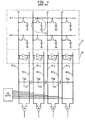
- Fig. 1 shows a portion of an array of memory cells 20 arranged in rows and columns.
- Array 20 includes a word line (WLi) per row and a "true” column conductor (BLTi) per column and a memory cell 21 connected at the intersection of each word line and bit line conductor, BLT.
- the array includes a section 30 for producing a complementary signal on a "complementary" bit line denoted as BLCi corresponding to each BLTi whereby each column includes a "true" bit-line (BLT) and a paired “complement” bit-line (BLC).
- SA sense amplifier
- each BLTi is the same distance from its paired BLCi as it is from the BLC(i-1) of the adjacent column, as illustrated in Fig. 2.
- the capacitance C INT between a pair of bit-lines (BLTi and BLCi) associated with the column Ci is generally equal to the capacitance (C EXT ) between the bit lines of adjacent columns [BLTi and BLC(i-1)].
- VDD/2 a voltage
- VDD voltage
- bit lines of the memory are driven to a high or low condition, with BLCi always driven to be the complement of BLTi.
- bit-lines are again driven to VDD/2, as noted above, and as shown in Fig. 2A.
- EP 0,697,735 discloses a single twist layout and method for an integrated circuit comprising a plurality of paired line conductors extending principally parallel. This invention is intended for such an interconnection array wherein intra-pair capacitive coupling is avoided and inter-pair capacitive couplings are matched.
- US 5,610,871 discloses a memory including sub-bit lines arranged corresponding to respective memory cell column groups and also includes master bit lines.
- C INT capacitance between the two bit lines (defining a pair of bit lines) of a column and there exists a certain amount of capacitance (C EXT ) between the bit lines of adjacent columns.
- C EXT capacitance
- Applicant's invention also resides in modifying the layout of the bit lines of the array whereby the capacitance (C INT ) of the paired bit lines is decreased even if this causes an increase in the capacitance (C EXT ) between adjacent bit lines.
- the invention may be best understood by noting the following:
- FIG. 6 A sketch of Q (D) as a function of D/S is shown in Fig. 6.
- the minimum charging current is obtained for a ratio of D/S equal to 0.172.
- charge current and power dissipation is decreased by increasing the spacing between the paired bit lines (BLTi and BLCi) and decreasing the spacing between the bit lines of adjacent columns [BLC(i-1) and BLTi; or BLCi and BLT(i+1)].
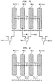
- a hierarchical bit-line architecture (as shown in Fig. 7A) permits double-pitch (2P)layout of the master bit lines coupling the outputs of the bit lines to sense amplifiers as shown in Figs. 7B and 7C.
- Bit-lines (BL) on a particular level may be coupled via switches 71 to a master bit-line (MBL) on a higher level as shown in Figs. 7A and 7B.
- MBL master bit-line
- each sense amplifier has a master bit-line (MBLT) for carrying data and a complementary bit-line (MBLC) for carrying the complementary data coupled to its outputs.
- CINT The capacitance between paired master bit-lines (MBLTi and MBLCi) is defined as CINT and the capacitance between the master bit-lines of adjacent columns is defined as CEXT.
- CINT is equal to CEXT, with each one of CINT and CEXT being equal to K/2P, where K is a technology dependent constant.
- Q charge needed to charge up these capacitances is as expressed in equation 1, above.
- the total charge required to charge the internal capacitances, CINT, (and hence the charging current for the bit lines) is decreased by moving the paired bit-lines (i.e., MBLTi and MBLCi) feeding the same sense amplifier (SAi) further apart while decreasing the spacing between the bit lines of adjacent columns, as shown in FIG. 8.
- SAi sense amplifier
- the spacing requirement is increased slightly (1.66P versus 2P for the minimum space). However, the spacing requirement is still not critical; critical levels would arise for requirements to use single pitch (1P), or less.
- Fig. 8 illustrates the skewing of the master bit lines. However, it should be evident that skewing of both the bit lines and the master bit lines can be done.
- the master bit lines are preferably formed on a master bit line (MBL) layer formed on top of a bit line (BL) layer containing the bit lines, similar to the showing in Fig. 7A.
- MBL master bit line
- One or more BLT lines may be coupled to an MBLT line and one or more BLC lines may be coupled to an MBLC line, as shown in Fig. 8A. That is, each master bit line (MBL) carries the data of two or more bit lines (BLs).
- a simple multiplex transistor may be inserted between the bit lines and the corresponding MBL, as shown in Fig. 8A. The selection of which BL gets connected to an MBL is accomplished by simple address decoding.
- the BLT and BLC lines are formed on a first level of a semiconductor chip with the BLC i s being defined by connecting inverters between the BLT i s and the corresponding BLC i s.
- the BLTs may be connected to respective MBLTs on a second level and the BLCs may be connected to respective MBLCs, also on the second level.
- the MBLCs may be defined from the underlying BLC and/or by the connection of inverters between corresponding MBLTs and MBLCs, as shown in Fig. 8B.
- the spacing between bit-lines and/or master bit-lines can be controlled (increased and/or decreased) to reduce the charging currents required to (pre) charge the bit-lines and/or the master bit-lines.
Landscapes
- Engineering & Computer Science (AREA)
- Computer Hardware Design (AREA)
- Microelectronics & Electronic Packaging (AREA)
- Dram (AREA)
- Semiconductor Memories (AREA)
- Static Random-Access Memory (AREA)
- Read Only Memory (AREA)
- Design And Manufacture Of Integrated Circuits (AREA)
Claims (11)
- Circuit intégré (IC) comprenant un réseau (20) de cellules de mémoire (21) disposées en rangées et en colonnes, ce circuit comprenant une paire de lignes de bits par colonne de cellules de mémoire, la paire de lignes par colonne étant destinées à transporter les données d'une cellule (21) et son complément, les lignes de bits étant disposées le long d'un niveau du circuit intégré, une capacité CINT existant entre les lignes de bits disposées par paires, et une capacité CEXT existant entre chacune des lignes de bits d'une paire et les lignes de bits d'une paire et les lignes de bits de colonnes adjacentes,
caractérisé en ce que
l'espacement entre les lignes de bits disposées par paires est supérieur à l'espacement entre les lignes de bits de chaque paire et les lignes de bits de colonnes adjacentes. - Circuit intégré selon la revendication 1,
dans lequel
les lignes de bits sont espacées de façon que la capacité CINT entre les lignes de bits disposées par paires soit inférieure à la capacité CEXT entre les lignes de bits disposées par paires d'une colonne et les lignes de bits adjacentes de colonnes adjacentes. - Circuit intégré selon la revendication 1,
dans lequelles lignes de bits sont préchargées avant chaque cycle de lecture ; etil faut moins de courant pour charger les lignes de bits dans le cas où CINT est inférieure à CEXT, que dans le cas où CINT est égale ou supérieure à CEXT. - Circuit intégré selon la revendication 1,
dans lequel
les lignes de bits sont des lignes de bits mères. - Circuit intégré selon la revendication 1,
dans lequel
les lignes de bits sont connectées directement aux cellules de mémoire du réseau. - Circuit intégré selon la revendication 4,
dans lequel
les lignes de bits mères sont couplées aux cellules de mémoire du réseau par l'intermédiaire de lignes de bits auxiliaires. - Circuit intégré selon la revendication 5,
dans lequelles lignes de bits sont disposées sur un premier niveau du circuit intégré,le circuit intégré comprend un second niveau,les lignes de bits mères sont disposées sur ce second niveau et connectées par des moyens de commutation (71) aux lignes de bits du premier niveau,les lignes de bits mères sont disposées par paires, chaque paire de lignes de bits mères étant destinée à transporter les données d'une cellule (21) et son complément, etl'espacement entre chaque ligne de bits mère disposée par paire, est supérieur à l'espacement entre les lignes de bits mères disposées par paires et les lignes de bits mères adjacentes. - Circuit intégré selon la revendication 6,
dans lequelles lignes de bits auxiliaires sont disposées à l'intérieur d'un premier niveau du circuit intégré et ces lignes de bits auxiliaires sont disposées par paires de façon qu'on ait une paire de lignes de bits auxiliaires par colonne de cellules de mémoire, une ligne de bits auxiliaire d'une paire étant destinée à transporter les données contenues dans les cellules de mémoire de sa colonne associée, et l'autre ligne de bits auxiliaire d'une paire étant destinée à transporter le complément de ces données,les lignes de bits mères (MBL) sont disposées à l'intérieur d'un second niveau du circuit intégré de façon que ces lignes de bits mères soient couplées à un nombre prédéterminé de lignes de bits auxiliaires, les lignes de bits mères étant disposées par paires de façon qu'une MBL d'une paire soit destinée à transporter les données d'une ou plusieurs lignes de bits auxiliaires et que l'autre MBL d'une paire soit destinée à transporter le complément de ces données ;il existe une capacité MCINT entre les lignes de bits mères disposées par paires, et une capacité MCEXT entre les lignes de bits mères d'une paire de lignes de bits mères, et les lignes de bits mères adjacentes ; etl'espacement entre les lignes de bits mères disposées par paires est supérieur à l'espacement entre les lignes de bits mères de chaque paire et les lignes de bits mères des colonnes adjacentes. - Circuit intégré selon la revendication 8,
dans lequel
les lignes de bits mères sont espacées de façon que la capacité MCINT entre lignes de bits mères disposées par paires, soit inférieure à la capacité MCEXT entre lignes de bits mères disposées par paires et les lignes de bits mères adjacentes. - Circuit intégré selon la revendication 8,
dans lequelles lignes de bits mères sont préchargées avant chaque cycle de lecture, etil faut moins de courant pour charger les lignes de bits mères dans le cas où MCINT est inférieure à MCEXT, que dans le cas où MCINT est égale ou supérieure à MCEXT. - Procédé destiné à diminuer le courant de charge nécessaire pour charger un réseau (20) de cellules de mémoire (21) dans un circuit intégré (IC), dans lequel le réseau de cellules de mémoire est disposé en rangées et en colonnes et comprend une paire de lignes de bits par colonne de cellules de mémoire, la paire de lignes de bits par colonne étant destinée à transporter les données d'une cellule (21) et son complément, les lignes de bits étant disposées le long d'un niveau de circuit intégré, une capacité CINT existant entre lignes de bits disposées par paires, et une capacité CEXT existant entre chacune des lignes de bits d'une paire et les lignes de bits de colonnes adjacentes,
caractérisé en ce que
l'espacement des lignes de bits est tel que l'espacement entre les lignes de bits disposées par paires soit supérieur à l'espacement entre les lignes de bits de chaque paire et les lignes de bits de colonnes adjacentes.
Applications Claiming Priority (2)
| Application Number | Priority Date | Filing Date | Title |
|---|---|---|---|
| US08/992,379 US5847986A (en) | 1997-12-17 | 1997-12-17 | Memory array with reduced charging current |
| US992379 | 1997-12-17 |
Publications (3)
| Publication Number | Publication Date |
|---|---|
| EP0924710A2 EP0924710A2 (fr) | 1999-06-23 |
| EP0924710A3 EP0924710A3 (fr) | 1999-09-29 |
| EP0924710B1 true EP0924710B1 (fr) | 2005-07-27 |
Family
ID=25538272
Family Applications (1)
| Application Number | Title | Priority Date | Filing Date |
|---|---|---|---|
| EP98120052A Expired - Lifetime EP0924710B1 (fr) | 1997-12-17 | 1998-10-23 | Réseau de mémoire avec courant de charge réduit |
Country Status (7)
| Country | Link |
|---|---|
| US (1) | US5847986A (fr) |
| EP (1) | EP0924710B1 (fr) |
| JP (1) | JPH11251551A (fr) |
| KR (1) | KR100591511B1 (fr) |
| CN (1) | CN1171238C (fr) |
| DE (1) | DE69830972T2 (fr) |
| TW (1) | TW409259B (fr) |
Families Citing this family (1)
| Publication number | Priority date | Publication date | Assignee | Title |
|---|---|---|---|---|
| US11222691B2 (en) * | 2020-03-09 | 2022-01-11 | Mediatek Inc. | Double-pitch-layout techniques and apparatus thereof |
Family Cites Families (6)
| Publication number | Priority date | Publication date | Assignee | Title |
|---|---|---|---|---|
| US5214601A (en) * | 1986-12-11 | 1993-05-25 | Mitsubishi Denki Kabushiki Kaisha | Bit line structure for semiconductor memory device including cross-points and multiple interconnect layers |
| US4975874B1 (en) * | 1988-11-01 | 1997-09-23 | Texas Instruments Inc | Metrix interconnection system with different width conductors |
| US5214600A (en) * | 1989-12-30 | 1993-05-25 | Samsung Electronics Co., Ltd. | Semiconductor memory array having interdigitated bit-line structure |
| JPH06334138A (ja) * | 1993-03-26 | 1994-12-02 | Sony Corp | 半導体記憶装置 |
| JP3672946B2 (ja) * | 1993-11-30 | 2005-07-20 | 株式会社ルネサステクノロジ | 半導体記憶装置 |
| EP0697735B1 (fr) * | 1994-08-15 | 2002-03-27 | International Business Machines Corporation | Arrangement à region torsadée unique et méthode pour des lignes conductrices arrangées par paires dans les circuits intégrés |
-
1997
- 1997-12-17 US US08/992,379 patent/US5847986A/en not_active Expired - Lifetime
-
1998
- 1998-10-23 EP EP98120052A patent/EP0924710B1/fr not_active Expired - Lifetime
- 1998-10-23 DE DE69830972T patent/DE69830972T2/de not_active Expired - Lifetime
- 1998-10-27 TW TW087117796A patent/TW409259B/zh not_active IP Right Cessation
- 1998-11-19 CN CNB981225152A patent/CN1171238C/zh not_active Expired - Fee Related
- 1998-11-25 KR KR1019980050602A patent/KR100591511B1/ko not_active Expired - Fee Related
- 1998-12-16 JP JP10358177A patent/JPH11251551A/ja not_active Withdrawn
Also Published As
| Publication number | Publication date |
|---|---|
| KR19990062600A (ko) | 1999-07-26 |
| DE69830972T2 (de) | 2006-05-24 |
| CN1171238C (zh) | 2004-10-13 |
| DE69830972D1 (de) | 2005-09-01 |
| US5847986A (en) | 1998-12-08 |
| CN1222739A (zh) | 1999-07-14 |
| TW409259B (en) | 2000-10-21 |
| KR100591511B1 (ko) | 2006-09-22 |
| EP0924710A3 (fr) | 1999-09-29 |
| EP0924710A2 (fr) | 1999-06-23 |
| JPH11251551A (ja) | 1999-09-17 |
Similar Documents
| Publication | Publication Date | Title |
|---|---|---|
| US5495440A (en) | Semiconductor memory device having hierarchical bit line structure | |
| US5602793A (en) | Semiconductor memory device having power line arranged in a meshed shape | |
| US4367540A (en) | Dynamic memory with an interchangeable pair of data lines and sense amplifiers | |
| KR930001554B1 (ko) | 다이나믹 반도체 기억장치와 그 구동방법 | |
| EP0273639B1 (fr) | Mémoire semi-conductrice à structure de mémorisation à niveaux multiples | |
| EP0393347A2 (fr) | DRAM avec lignes de bit blindées contre la diaphonie | |
| US20050133852A1 (en) | High performance embedded semiconductor memory devices with multiple dimension first-level bit-lines | |
| EP0077935B1 (fr) | Dispositif de mémoire dynamique | |
| US5933363A (en) | Associative memory having comparator for detecting data match signal | |
| JPS5826830B2 (ja) | 集積回路メモリ・アレイ | |
| US4086662A (en) | Memory system with read/write control lines | |
| EP0185451B1 (fr) | Dispositif de mémoire semi-conductrice avec des amplificateurs de détection | |
| EP0264929A2 (fr) | Dispositif de mémoire à semi-conducteurs avec une disposition modifiée de lignes de bit | |
| US5966340A (en) | Semiconductor memory device having hierarchical word line structure | |
| US7009880B1 (en) | Non-volatile memory architecture to improve read performance | |
| EP0089720B1 (fr) | Mémoire RAM à transistor et condensateur unique | |
| JPS5894188A (ja) | 増幅装置 | |
| US6759280B2 (en) | Memory device with divided bit-line architecture | |
| US4520466A (en) | Dynamic random access memory | |
| JPS6027116B2 (ja) | 未知の電荷の感知装置 | |
| US6310811B1 (en) | Memory with high speed reading operation using a switchable reference matrix ensuring charging speed | |
| EP0186745A2 (fr) | Matrice de mémoire | |
| EP0037262B1 (fr) | Dispositif de mémoire à semi-conducteurs | |
| EP0036932B1 (fr) | Système de détection de données et mémoire utilisant ce système | |
| EP0276854A2 (fr) | Dispositif de mémoire à semi-conducteurs avec un schéma de sélection de colonnes |
Legal Events
| Date | Code | Title | Description |
|---|---|---|---|
| PUAI | Public reference made under article 153(3) epc to a published international application that has entered the european phase |
Free format text: ORIGINAL CODE: 0009012 |
|
| AK | Designated contracting states |
Kind code of ref document: A2 Designated state(s): DE FR GB IE IT NL |
|
| AX | Request for extension of the european patent |
Free format text: AL;LT;LV;MK;RO;SI |
|
| PUAL | Search report despatched |
Free format text: ORIGINAL CODE: 0009013 |
|
| AK | Designated contracting states |
Kind code of ref document: A3 Designated state(s): AT BE CH CY DE DK ES FI FR GB GR IE IT LI LU MC NL PT SE |
|
| AX | Request for extension of the european patent |
Free format text: AL;LT;LV;MK;RO;SI |
|
| 17P | Request for examination filed |
Effective date: 19991124 |
|
| AKX | Designation fees paid |
Free format text: DE FR GB IE IT NL |
|
| 17Q | First examination report despatched |
Effective date: 20030605 |
|
| RAP1 | Party data changed (applicant data changed or rights of an application transferred) |
Owner name: INFINEON TECHNOLOGIES AG |
|
| GRAP | Despatch of communication of intention to grant a patent |
Free format text: ORIGINAL CODE: EPIDOSNIGR1 |
|
| GRAS | Grant fee paid |
Free format text: ORIGINAL CODE: EPIDOSNIGR3 |
|
| GRAA | (expected) grant |
Free format text: ORIGINAL CODE: 0009210 |
|
| AK | Designated contracting states |
Kind code of ref document: B1 Designated state(s): DE FR GB IE IT NL |
|
| REG | Reference to a national code |
Ref country code: GB Ref legal event code: FG4D |
|
| REG | Reference to a national code |
Ref country code: IE Ref legal event code: FG4D |
|
| REF | Corresponds to: |
Ref document number: 69830972 Country of ref document: DE Date of ref document: 20050901 Kind code of ref document: P |
|
| PGFP | Annual fee paid to national office [announced via postgrant information from national office to epo] |
Ref country code: NL Payment date: 20051013 Year of fee payment: 8 |
|
| ET | Fr: translation filed | ||
| PLBE | No opposition filed within time limit |
Free format text: ORIGINAL CODE: 0009261 |
|
| REG | Reference to a national code |
Ref country code: HK Ref legal event code: WD Ref document number: 1018340 Country of ref document: HK |
|
| STAA | Information on the status of an ep patent application or granted ep patent |
Free format text: STATUS: NO OPPOSITION FILED WITHIN TIME LIMIT |
|
| 26N | No opposition filed |
Effective date: 20060428 |
|
| PGFP | Annual fee paid to national office [announced via postgrant information from national office to epo] |
Ref country code: GB Payment date: 20061023 Year of fee payment: 9 |
|
| PG25 | Lapsed in a contracting state [announced via postgrant information from national office to epo] |
Ref country code: NL Free format text: LAPSE BECAUSE OF NON-PAYMENT OF DUE FEES Effective date: 20070501 |
|
| NLV4 | Nl: lapsed or anulled due to non-payment of the annual fee |
Effective date: 20070501 |
|
| PGFP | Annual fee paid to national office [announced via postgrant information from national office to epo] |
Ref country code: IT Payment date: 20071026 Year of fee payment: 10 |
|
| PGFP | Annual fee paid to national office [announced via postgrant information from national office to epo] |
Ref country code: FR Payment date: 20071016 Year of fee payment: 10 |
|
| GBPC | Gb: european patent ceased through non-payment of renewal fee |
Effective date: 20071023 |
|
| PG25 | Lapsed in a contracting state [announced via postgrant information from national office to epo] |
Ref country code: GB Free format text: LAPSE BECAUSE OF NON-PAYMENT OF DUE FEES Effective date: 20071023 |
|
| REG | Reference to a national code |
Ref country code: IE Ref legal event code: MM4A |
|
| REG | Reference to a national code |
Ref country code: FR Ref legal event code: ST Effective date: 20090630 |
|
| PG25 | Lapsed in a contracting state [announced via postgrant information from national office to epo] |
Ref country code: IT Free format text: LAPSE BECAUSE OF NON-PAYMENT OF DUE FEES Effective date: 20081023 |
|
| PGFP | Annual fee paid to national office [announced via postgrant information from national office to epo] |
Ref country code: IE Payment date: 20071023 Year of fee payment: 10 |
|
| PG25 | Lapsed in a contracting state [announced via postgrant information from national office to epo] |
Ref country code: IE Free format text: LAPSE BECAUSE OF NON-PAYMENT OF DUE FEES Effective date: 20081023 Ref country code: FR Free format text: LAPSE BECAUSE OF NON-PAYMENT OF DUE FEES Effective date: 20081031 |
|
| PGFP | Annual fee paid to national office [announced via postgrant information from national office to epo] |
Ref country code: DE Payment date: 20141022 Year of fee payment: 17 |
|
| REG | Reference to a national code |
Ref country code: DE Ref legal event code: R081 Ref document number: 69830972 Country of ref document: DE Owner name: POLARIS INNOVATIONS LTD., IE Free format text: FORMER OWNER: QIMONDA AG, 81739 MUENCHEN, DE Ref country code: DE Ref legal event code: R081 Ref document number: 69830972 Country of ref document: DE Owner name: INFINEON TECHNOLOGIES AG, DE Free format text: FORMER OWNER: QIMONDA AG, 81739 MUENCHEN, DE |
|
| REG | Reference to a national code |
Ref country code: DE Ref legal event code: R081 Ref document number: 69830972 Country of ref document: DE Owner name: POLARIS INNOVATIONS LTD., IE Free format text: FORMER OWNER: INFINEON TECHNOLOGIES AG, 85579 NEUBIBERG, DE |
|
| REG | Reference to a national code |
Ref country code: DE Ref legal event code: R119 Ref document number: 69830972 Country of ref document: DE |
|
| PG25 | Lapsed in a contracting state [announced via postgrant information from national office to epo] |
Ref country code: DE Free format text: LAPSE BECAUSE OF NON-PAYMENT OF DUE FEES Effective date: 20160503 |