EP0924724A2 - Photoelectric conversion device and photo-electrochemical cell - Google Patents
Photoelectric conversion device and photo-electrochemical cell Download PDFInfo
- Publication number
- EP0924724A2 EP0924724A2 EP98122973A EP98122973A EP0924724A2 EP 0924724 A2 EP0924724 A2 EP 0924724A2 EP 98122973 A EP98122973 A EP 98122973A EP 98122973 A EP98122973 A EP 98122973A EP 0924724 A2 EP0924724 A2 EP 0924724A2
- Authority
- EP
- European Patent Office
- Prior art keywords
- photoelectric conversion
- dye
- conversion device
- electrolyte
- compounds
- Prior art date
- Legal status (The legal status is an assumption and is not a legal conclusion. Google has not performed a legal analysis and makes no representation as to the accuracy of the status listed.)
- Granted
Links
Images

Classifications
-
- H—ELECTRICITY
- H01—ELECTRIC ELEMENTS
- H01G—CAPACITORS; CAPACITORS, RECTIFIERS, DETECTORS, SWITCHING DEVICES, LIGHT-SENSITIVE OR TEMPERATURE-SENSITIVE DEVICES OF THE ELECTROLYTIC TYPE
- H01G9/00—Electrolytic capacitors, rectifiers, detectors, switching devices, light-sensitive or temperature-sensitive devices; Processes of their manufacture
- H01G9/20—Light-sensitive devices
- H01G9/2004—Light-sensitive devices characterised by the electrolyte, e.g. comprising an organic electrolyte
- H01G9/2009—Solid electrolytes
-
- C—CHEMISTRY; METALLURGY
- C09—DYES; PAINTS; POLISHES; NATURAL RESINS; ADHESIVES; COMPOSITIONS NOT OTHERWISE PROVIDED FOR; APPLICATIONS OF MATERIALS NOT OTHERWISE PROVIDED FOR
- C09B—ORGANIC DYES OR CLOSELY-RELATED COMPOUNDS FOR PRODUCING DYES, e.g. PIGMENTS; MORDANTS; LAKES
- C09B23/00—Methine or polymethine dyes, e.g. cyanine dyes
- C09B23/0008—Methine or polymethine dyes, e.g. cyanine dyes substituted on the polymethine chain
-
- C—CHEMISTRY; METALLURGY
- C09—DYES; PAINTS; POLISHES; NATURAL RESINS; ADHESIVES; COMPOSITIONS NOT OTHERWISE PROVIDED FOR; APPLICATIONS OF MATERIALS NOT OTHERWISE PROVIDED FOR
- C09B—ORGANIC DYES OR CLOSELY-RELATED COMPOUNDS FOR PRODUCING DYES, e.g. PIGMENTS; MORDANTS; LAKES
- C09B23/00—Methine or polymethine dyes, e.g. cyanine dyes
- C09B23/0008—Methine or polymethine dyes, e.g. cyanine dyes substituted on the polymethine chain
- C09B23/0016—Methine or polymethine dyes, e.g. cyanine dyes substituted on the polymethine chain the substituent being a halogen atom
-
- C—CHEMISTRY; METALLURGY
- C09—DYES; PAINTS; POLISHES; NATURAL RESINS; ADHESIVES; COMPOSITIONS NOT OTHERWISE PROVIDED FOR; APPLICATIONS OF MATERIALS NOT OTHERWISE PROVIDED FOR
- C09B—ORGANIC DYES OR CLOSELY-RELATED COMPOUNDS FOR PRODUCING DYES, e.g. PIGMENTS; MORDANTS; LAKES
- C09B23/00—Methine or polymethine dyes, e.g. cyanine dyes
- C09B23/0008—Methine or polymethine dyes, e.g. cyanine dyes substituted on the polymethine chain
- C09B23/0025—Methine or polymethine dyes, e.g. cyanine dyes substituted on the polymethine chain the substituent being bound through an oxygen atom
-
- C—CHEMISTRY; METALLURGY
- C09—DYES; PAINTS; POLISHES; NATURAL RESINS; ADHESIVES; COMPOSITIONS NOT OTHERWISE PROVIDED FOR; APPLICATIONS OF MATERIALS NOT OTHERWISE PROVIDED FOR
- C09B—ORGANIC DYES OR CLOSELY-RELATED COMPOUNDS FOR PRODUCING DYES, e.g. PIGMENTS; MORDANTS; LAKES
- C09B23/00—Methine or polymethine dyes, e.g. cyanine dyes
- C09B23/0008—Methine or polymethine dyes, e.g. cyanine dyes substituted on the polymethine chain
- C09B23/0041—Methine or polymethine dyes, e.g. cyanine dyes substituted on the polymethine chain the substituent being bound through a nitrogen atom
-
- C—CHEMISTRY; METALLURGY
- C09—DYES; PAINTS; POLISHES; NATURAL RESINS; ADHESIVES; COMPOSITIONS NOT OTHERWISE PROVIDED FOR; APPLICATIONS OF MATERIALS NOT OTHERWISE PROVIDED FOR
- C09B—ORGANIC DYES OR CLOSELY-RELATED COMPOUNDS FOR PRODUCING DYES, e.g. PIGMENTS; MORDANTS; LAKES
- C09B23/00—Methine or polymethine dyes, e.g. cyanine dyes
- C09B23/0066—Methine or polymethine dyes, e.g. cyanine dyes the polymethine chain being part of a carbocyclic ring,(e.g. benzene, naphtalene, cyclohexene, cyclobutenene-quadratic acid)
-
- C—CHEMISTRY; METALLURGY
- C09—DYES; PAINTS; POLISHES; NATURAL RESINS; ADHESIVES; COMPOSITIONS NOT OTHERWISE PROVIDED FOR; APPLICATIONS OF MATERIALS NOT OTHERWISE PROVIDED FOR
- C09B—ORGANIC DYES OR CLOSELY-RELATED COMPOUNDS FOR PRODUCING DYES, e.g. PIGMENTS; MORDANTS; LAKES
- C09B23/00—Methine or polymethine dyes, e.g. cyanine dyes
- C09B23/0075—Methine or polymethine dyes, e.g. cyanine dyes the polymethine chain being part of an heterocyclic ring
-
- C—CHEMISTRY; METALLURGY
- C09—DYES; PAINTS; POLISHES; NATURAL RESINS; ADHESIVES; COMPOSITIONS NOT OTHERWISE PROVIDED FOR; APPLICATIONS OF MATERIALS NOT OTHERWISE PROVIDED FOR
- C09B—ORGANIC DYES OR CLOSELY-RELATED COMPOUNDS FOR PRODUCING DYES, e.g. PIGMENTS; MORDANTS; LAKES
- C09B23/00—Methine or polymethine dyes, e.g. cyanine dyes
- C09B23/02—Methine or polymethine dyes, e.g. cyanine dyes the polymethine chain containing an odd number of >CH- or >C[alkyl]- groups
- C09B23/04—Methine or polymethine dyes, e.g. cyanine dyes the polymethine chain containing an odd number of >CH- or >C[alkyl]- groups one >CH- group, e.g. cyanines, isocyanines, pseudocyanines
-
- C—CHEMISTRY; METALLURGY
- C09—DYES; PAINTS; POLISHES; NATURAL RESINS; ADHESIVES; COMPOSITIONS NOT OTHERWISE PROVIDED FOR; APPLICATIONS OF MATERIALS NOT OTHERWISE PROVIDED FOR
- C09B—ORGANIC DYES OR CLOSELY-RELATED COMPOUNDS FOR PRODUCING DYES, e.g. PIGMENTS; MORDANTS; LAKES
- C09B23/00—Methine or polymethine dyes, e.g. cyanine dyes
- C09B23/02—Methine or polymethine dyes, e.g. cyanine dyes the polymethine chain containing an odd number of >CH- or >C[alkyl]- groups
- C09B23/06—Methine or polymethine dyes, e.g. cyanine dyes the polymethine chain containing an odd number of >CH- or >C[alkyl]- groups three >CH- groups, e.g. carbocyanines
-
- C—CHEMISTRY; METALLURGY
- C09—DYES; PAINTS; POLISHES; NATURAL RESINS; ADHESIVES; COMPOSITIONS NOT OTHERWISE PROVIDED FOR; APPLICATIONS OF MATERIALS NOT OTHERWISE PROVIDED FOR
- C09B—ORGANIC DYES OR CLOSELY-RELATED COMPOUNDS FOR PRODUCING DYES, e.g. PIGMENTS; MORDANTS; LAKES
- C09B23/00—Methine or polymethine dyes, e.g. cyanine dyes
- C09B23/02—Methine or polymethine dyes, e.g. cyanine dyes the polymethine chain containing an odd number of >CH- or >C[alkyl]- groups
- C09B23/08—Methine or polymethine dyes, e.g. cyanine dyes the polymethine chain containing an odd number of >CH- or >C[alkyl]- groups more than three >CH- groups, e.g. polycarbocyanines
- C09B23/083—Methine or polymethine dyes, e.g. cyanine dyes the polymethine chain containing an odd number of >CH- or >C[alkyl]- groups more than three >CH- groups, e.g. polycarbocyanines five >CH- groups
-
- C—CHEMISTRY; METALLURGY
- C09—DYES; PAINTS; POLISHES; NATURAL RESINS; ADHESIVES; COMPOSITIONS NOT OTHERWISE PROVIDED FOR; APPLICATIONS OF MATERIALS NOT OTHERWISE PROVIDED FOR
- C09B—ORGANIC DYES OR CLOSELY-RELATED COMPOUNDS FOR PRODUCING DYES, e.g. PIGMENTS; MORDANTS; LAKES
- C09B23/00—Methine or polymethine dyes, e.g. cyanine dyes
- C09B23/02—Methine or polymethine dyes, e.g. cyanine dyes the polymethine chain containing an odd number of >CH- or >C[alkyl]- groups
- C09B23/08—Methine or polymethine dyes, e.g. cyanine dyes the polymethine chain containing an odd number of >CH- or >C[alkyl]- groups more than three >CH- groups, e.g. polycarbocyanines
- C09B23/086—Methine or polymethine dyes, e.g. cyanine dyes the polymethine chain containing an odd number of >CH- or >C[alkyl]- groups more than three >CH- groups, e.g. polycarbocyanines more than five >CH- groups
-
- C—CHEMISTRY; METALLURGY
- C09—DYES; PAINTS; POLISHES; NATURAL RESINS; ADHESIVES; COMPOSITIONS NOT OTHERWISE PROVIDED FOR; APPLICATIONS OF MATERIALS NOT OTHERWISE PROVIDED FOR
- C09B—ORGANIC DYES OR CLOSELY-RELATED COMPOUNDS FOR PRODUCING DYES, e.g. PIGMENTS; MORDANTS; LAKES
- C09B23/00—Methine or polymethine dyes, e.g. cyanine dyes
- C09B23/14—Styryl dyes
- C09B23/145—Styryl dyes the ethylene chain carrying an heterocyclic residue, e.g. heterocycle-CH=CH-C6H5
-
- H—ELECTRICITY
- H01—ELECTRIC ELEMENTS
- H01G—CAPACITORS; CAPACITORS, RECTIFIERS, DETECTORS, SWITCHING DEVICES, LIGHT-SENSITIVE OR TEMPERATURE-SENSITIVE DEVICES OF THE ELECTROLYTIC TYPE
- H01G9/00—Electrolytic capacitors, rectifiers, detectors, switching devices, light-sensitive or temperature-sensitive devices; Processes of their manufacture
- H01G9/20—Light-sensitive devices
-
- H—ELECTRICITY
- H01—ELECTRIC ELEMENTS
- H01G—CAPACITORS; CAPACITORS, RECTIFIERS, DETECTORS, SWITCHING DEVICES, LIGHT-SENSITIVE OR TEMPERATURE-SENSITIVE DEVICES OF THE ELECTROLYTIC TYPE
- H01G9/00—Electrolytic capacitors, rectifiers, detectors, switching devices, light-sensitive or temperature-sensitive devices; Processes of their manufacture
- H01G9/20—Light-sensitive devices
- H01G9/2027—Light-sensitive devices comprising an oxide semiconductor electrode
- H01G9/2031—Light-sensitive devices comprising an oxide semiconductor electrode comprising titanium oxide, e.g. TiO2
-
- H—ELECTRICITY
- H01—ELECTRIC ELEMENTS
- H01G—CAPACITORS; CAPACITORS, RECTIFIERS, DETECTORS, SWITCHING DEVICES, LIGHT-SENSITIVE OR TEMPERATURE-SENSITIVE DEVICES OF THE ELECTROLYTIC TYPE
- H01G9/00—Electrolytic capacitors, rectifiers, detectors, switching devices, light-sensitive or temperature-sensitive devices; Processes of their manufacture
- H01G9/20—Light-sensitive devices
- H01G9/2059—Light-sensitive devices comprising an organic dye as the active light absorbing material, e.g. adsorbed on an electrode or dissolved in solution
-
- H—ELECTRICITY
- H10—SEMICONDUCTOR DEVICES; ELECTRIC SOLID-STATE DEVICES NOT OTHERWISE PROVIDED FOR
- H10K—ORGANIC ELECTRIC SOLID-STATE DEVICES
- H10K85/00—Organic materials used in the body or electrodes of devices covered by this subclass
- H10K85/30—Coordination compounds
- H10K85/341—Transition metal complexes, e.g. Ru(II)polypyridine complexes
- H10K85/344—Transition metal complexes, e.g. Ru(II)polypyridine complexes comprising ruthenium
-
- H—ELECTRICITY
- H10—SEMICONDUCTOR DEVICES; ELECTRIC SOLID-STATE DEVICES NOT OTHERWISE PROVIDED FOR
- H10K—ORGANIC ELECTRIC SOLID-STATE DEVICES
- H10K85/00—Organic materials used in the body or electrodes of devices covered by this subclass
- H10K85/60—Organic compounds having low molecular weight
- H10K85/649—Aromatic compounds comprising a hetero atom
- H10K85/652—Cyanine dyes
-
- Y—GENERAL TAGGING OF NEW TECHNOLOGICAL DEVELOPMENTS; GENERAL TAGGING OF CROSS-SECTIONAL TECHNOLOGIES SPANNING OVER SEVERAL SECTIONS OF THE IPC; TECHNICAL SUBJECTS COVERED BY FORMER USPC CROSS-REFERENCE ART COLLECTIONS [XRACs] AND DIGESTS
- Y02—TECHNOLOGIES OR APPLICATIONS FOR MITIGATION OR ADAPTATION AGAINST CLIMATE CHANGE
- Y02E—REDUCTION OF GREENHOUSE GAS [GHG] EMISSIONS, RELATED TO ENERGY GENERATION, TRANSMISSION OR DISTRIBUTION
- Y02E10/00—Energy generation through renewable energy sources
- Y02E10/50—Photovoltaic [PV] energy
- Y02E10/542—Dye sensitized solar cells
-
- Y—GENERAL TAGGING OF NEW TECHNOLOGICAL DEVELOPMENTS; GENERAL TAGGING OF CROSS-SECTIONAL TECHNOLOGIES SPANNING OVER SEVERAL SECTIONS OF THE IPC; TECHNICAL SUBJECTS COVERED BY FORMER USPC CROSS-REFERENCE ART COLLECTIONS [XRACs] AND DIGESTS
- Y02—TECHNOLOGIES OR APPLICATIONS FOR MITIGATION OR ADAPTATION AGAINST CLIMATE CHANGE
- Y02E—REDUCTION OF GREENHOUSE GAS [GHG] EMISSIONS, RELATED TO ENERGY GENERATION, TRANSMISSION OR DISTRIBUTION
- Y02E10/00—Energy generation through renewable energy sources
- Y02E10/50—Photovoltaic [PV] energy
- Y02E10/549—Organic PV cells
Definitions
- This invention relates to a photoelectric converter, and more particularly, to a photoelectric converter comprising a dye-sensitized nanoparticulate semiconductor. It also relates to a photo-electrochemical cell.
- An object of the present invention is to provide a dye-sensitized photoelectric converter having improved photoelectric conversion characteristics and durability. Another object of the present invention is to provide a photo-regenerative photo-electrochemical cell using the same.
- the invention provides a photoelectric conversion device comprising a conductive support, a layer coated on the conductive support and containing semiconductor nanoparticulates having a dye adsorbed thereto, a gel electrolyte-containing layer, and a counter electrode.
- the gel electrolyte contains an electrolyte and a gelling agent having a molecular weight of up to 1,000.
- the electrolyte comprises a metal iodide, iodide salt of quaternary ammonium compound, iodide salt of quaternary imidazolium compound, iodide salt of quaternary pyridinium compound, metal bromide, bromide salt of quaternary ammonium compound, sulfur compound, viologen dye, or hydroquinone-quinone.
- the electrolyte may contain iodine.
- the electrolyte is preferably present in a concentration of 0.05 to 1.5 mol/liter of the gel electrolyte.
- the gelling agent is preferably present in a concentration of 0.2 to 500 g/liter of the gel electrolyte.
- the gel electrolyte may further contain at least one organic solvent selected from among nitrile compounds, carbonate compounds, nitrogenous heterocyclic compounds, and ethylene glycol dialkyl ethers.
- the dye is typically a ruthenium complex dye or polymethine dye.
- Also contemplated herein is a photo-electrochemical cell comprising the photoelectric conversion device.
- the dye-sensitized photoelectric converter device is defined as comprising a conductive support, a layer coated on the conductive support and containing semiconductor nanoparticulates having a dye adsorbed thereto, which is also referred to as a photosensitive layer, a gel electrolyte-containing layer, and a counter electrode.
- the gel electrolyte contains an electrolyte and a gelling agent having a molecular weight of up to 1,000.
- the gelling agent used herein is a compound which when added to an organic solvent in a concentration of up to 500 g/liter, can solidify or gel the entire system.
- incorporación of the gelling agent having a molecular weight of up to 1,000 into the gel electrolyte-containing layer ensures the manufacture of a photoelectric converter device having improved photoelectric conversion characteristics and durability as demonstrated by a high short-circuit current density and no degradation with time of short-circuit current density.
- use of an electrolyte solution instead of the gel electrolyte invites a substantial degradation with time; and use of an electrolyte comprising as a matrix a crosslinked polymeric gel in which a crosslinking agent serves as a gelling agent results in a low short-circuit current density.
- the conductive supports used herein include metal supports which have conductivity in themselves and glass or plastic supports having a conductive agent layer on their surface.
- preferred conductive agents are metals such as platinum, gold, silver, copper, aluminum, rhodium, and indium, carbon, and conductive metal oxides such as indium-tin composite oxides and fluorine-doped tin oxide.
- conductive glass supports in the form of transparent substrates of low cost sodalime float glass having deposited thereon a conductive layer of fluorine-doped tin dioxide.
- the conductive layer preferably has a thickness of about 0.02 to about 10 ⁇ m.
- the conductive supports have a lower surface resistivity.
- the preferred range of surface resistivity is up to 100 ⁇ /cm 2 , more preferably up to 40 ⁇ /cm 2 .
- the lower limit of the surface resistivity is not critical although it is usually about 0.1 ⁇ /cm 2 .
- the conductive supports be substantially transparent.
- substantially transparent means that the light transmittance of the support is at least 10%, preferably at least 50%, more preferably at least 70%.
- glass or plastic supports having conductive metal oxide coated thereon are preferable.
- the coverage or weight of conductive metal oxide coated is preferably 0.01 to 100 g per square meter of the glass or plastic support. Where transparent conductive supports are used, it is desired that light enter the device from the support side.
- nanoparticulates of metal chalcogenides e.g., oxides, sulfides and selenides
- perovskite examples include oxides of titanium, tin, zinc, tungsten, zirconium, hafnium, strontium, indium, cerium, yttrium, lanthanum, vanadium, niobium, and tantalum, cadmium sulfide, and cadmium selenide.
- Preferred examples of the perovskite are strontium titanate and calcium titanate. Of these, titanium oxide, zinc oxide, tin oxide and tungsten oxide are especially preferred.
- the semiconductor nanoparticulates preferably have a mean particle size of 5 to 200 nm, more preferably 8 to 100 nm, expressed by the diameter of a circle of equivalent area to the projected area of a primary particle. Also preferably, the semiconductor particles in the dispersion have a mean particle size of 0.01 to 100 ⁇ m.
- Exemplary methods are a method of applying a dispersion liquid or colloid solution of semiconductor nanoparticulates onto a conductive support, and a method (known as sol-gel method) of applying a semiconductor nanoparticulate precursor onto a conductive support and allowing the precursor to be hydrolyzed with moisture in air and condensed, thereby forming a semiconductor nanoparticulate coating.
- the dispersion liquid of semiconductor nanoparticulates can be prepared by the sol-gel method and other methods such as grinding in a mortar, milling and dispersing in a mill, and synthesizing a semiconductor under such conditions that the semiconductor may precipitate in a solvent as nanoparticulates.
- the dispersing media may be water or various organic solvents such as methanol, ethanol, isopropanol, dichloromethane, acetone, acetonitrile, and ethyl acetate.
- organic solvents such as methanol, ethanol, isopropanol, dichloromethane, acetone, acetonitrile, and ethyl acetate.
- polymers, surfactants, acids or chelates may be used as the dispersant if necessary.
- Semiconductor nanoparticulates are desired to have a greater surface area so that more dye may be adsorbed thereon.
- the semiconductor nanoparticulates as applied onto the support to form a layer should preferably have a surface area which is greater than the projected area by a factor of at least 10, more preferably at least 100. No upper limit is imposed on the surface area although the upper limit is usually a multiplication factor of about 1,000.
- the semiconductor nanoparticulate layer has an appropriate range of thickness which is typically 0.1 to 100 ⁇ m.
- an appropriate thickness is 1 to 30 ⁇ m, especially 3 to 20 ⁇ m.
- semiconductor nanoparticulates may be fired in order to bring the particulates into electronic contact and improve the strength and the adhesion to the support of the coating.
- the preferred range of firing temperature is from 40°C to less than 700°C, more preferably 40°C to 650°C.
- the firing time is about 10 minutes to about 10 hours.
- the semiconductor nanoparticulates may be subject to chemical plating in an aqueous solution of titanium tetrachloride or electrochemical plating in an aqueous solution of titanium trichloride, for the purpose of increasing the surface area of semiconductor nanoparticulates or increasing the purity in the vicinity of semiconductor nanoparticulates for increasing the efficiency of electron injection from the dye into the semiconductor nanoparticulates.
- the coverage or weight of semiconductor nanoparticulates coated is preferably 0.5 to 500 g, more preferably 2 to 100 g per square meter of the support.
- the dyes also called chromophores or sensitizers, which are used in the present invention are preferably ruthenium complex dyes and/or polymethine dyes. Further preferably, the dyes have appropriate interlocking groups to surfaces of semiconductor nanoparticulates.
- Preferred interlocking groups include COOH, cyano, and PO 3 H 2 groups, as well as chelating groups having ⁇ -conducting character such as oximes, dioximes, hydroxyquinolines, salicylates, and alpha-keto enolates. Of these, COOH and PO 3 H 2 groups are especially preferred. These groups may form salts with alkali metals or intramolecular salts.
- ruthenium complex dyes are used in the practice of the invention, they are preferably of the following general formula (1).
- Xa na Ru(L 1 )(L 1a )
- Ru is ruthenium
- Xa is a ligand selected from the group consisting of Cl, SCN, H 2 O, Br, I, CN, -NCO, and SeCN
- letter na is equal to 1 or 2, preferably equal to 2
- L 1 and L 1a each are an organic ligand selected from the following ligands L-1 to L-9.
- Ra is hydrogen, a halogen atom or a substituted or unsubstituted alkyl, aralkyl or aryl group having 1 to 12 carbon atoms.
- the ruthenium complex dyes which can be used herein are, for example, the complex dyes described in USP 4,927,721, 4,684,537, 5,084,365, 5,350,644, 5,463,057, 5,525,440 and JP-A 249790/1995.
- polymethine dyes are used in the practice of the invention, they are preferably of the following general formula (2) or (3).
- Rb and Rf are independently hydrogen, alkyl groups, aryl groups or heterocyclic residues, Rc to Re are independently hydrogen or substituents. Alternatively, Rb to Rf, taken together, may form a ring.
- X 11 and X 12 are independently nitrogen, oxygen, sulfur, selenium or tellurium.
- Letters n 11 and n 13 are integers of 0 to 2, and n 12 is an integer of 1 to 6.
- the compound of formula (2) may have a counter ion if necessary from the overall electric charge of its molecule.
- Za is a group of non-metallic atoms necessary to form a nitrogenous heterocycle.
- Rg is an alkyl or aryl group.
- Q is a methine or polymethine group necessary for the compound of formula (3) to become a methine dye. It is noted that Za, Rg and Q represent groups which enable the compound of formula (3) to have at least one substituent of the general formula (4).
- X is a charge equilibrating counter ion.
- Letter n is a number of 0 to 10 necessary to neutralize the electric charge of the molecule.
- L is an oxygen atom, sulfur atom or imino group
- letter m 1 is equal to 0 or 1
- m 2 and m 3 each are equal to 0 or 1. Where m 2 or m 3 or both are 0, the substituent of formula (4) has a negative charge.
- polymethine dye Illustrative examples of the polymethine dye are described in M. Okawara, T. Kitao, T. Hirasima & M. Matuoka, "Organic Colorants” (Elsevier).
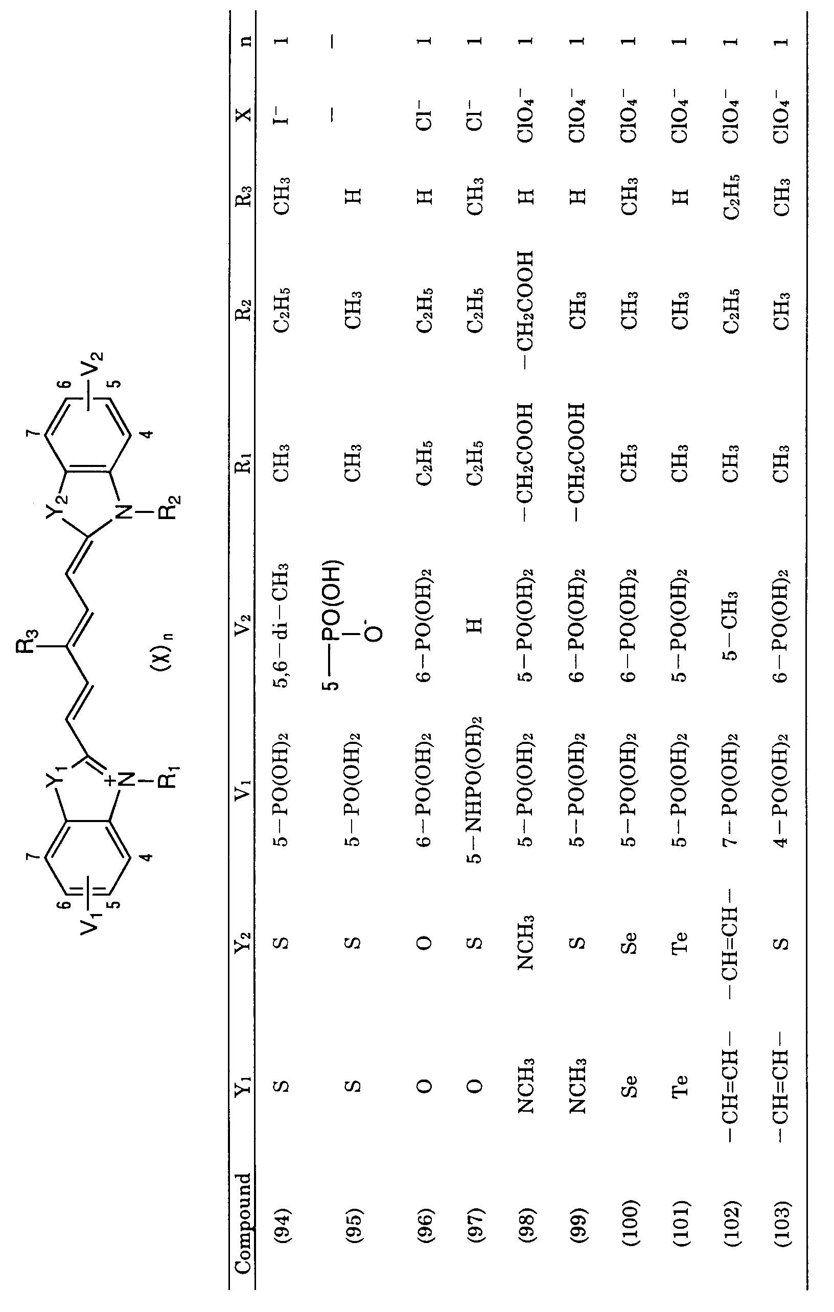
- polymethine dyes of general formulae (2) and (3) are given below.
- the compounds of general formulae (2) and (3) can be synthesized by the methods described in F.M. Harmer, Heterocyclic Compounds - Cyanine Dyes and Related Compounds, John Wiley & Sons, New York, London, 1964; D.M. Sturmer, Heterocyclic Compounds - Special topics in heterocyclic chemistry," Chap. 18, Sec. 14, pp. 482-515, John Wiley & Sons, New York, London, 1977; Rodd's Chemistry of Carbon Compounds, 2nd Ed., vol. IV, part B, 1977, Chap. 15, pp. 369-422, Elsevier Science Publishing Company Inc., New York; and British Patent No. 1,077,611.
- the dye is adsorbed to semiconductor nanoparticulates, most often by immersing fully dry semiconductor nanoparticulates in a dye solution for several hours.
- the dye adsorption may be done at room temperature or by heating under reflux as described in JP-A 249790/1995.
- the dye adsorption may be done either prior to or subsequent to the coating of semiconductor nanoparticulates. It is also acceptable that semiconductor nanoparticulates and the dye are simultaneously coated whereupon adsorption takes place. It is desirable to remove the unadsorbed dye by washing. Where the coated film is fired, it is preferred that the dye adsorption be done subsequent to firing. It is especially preferred that the dye is quickly adsorbed to the coated film after firing and before water adsorbs to the surface of the coated film.
- a single dye or a mixture of dyes may be used.
- dyes are selected and mixed so as to make the wavelength range of photoelectric conversion as broad as possible.
- the overall amount of the dye used is preferably 0.01 to 100 mmol per square meter of the support.
- the amount of the dye adsorbed to semiconductor nanoparticulates is preferably 0.01 to 1 mmol per gram of the semiconductor nanoparticulates.
- An amount of the dye in this range provides a sufficient semiconductor sensitizing effect. Less amounts of the dye would provide an insufficient sensitizing effect. If the amount of the dye is too much, the dye that is not adsorbed to the semiconductor would float, detracting from the sensitizing effect.
- a colorless compound may be co-adsorbed.
- Hydrophobic compounds to be co-adsorbed are steroid compounds having a carboxyl group, e.g., cholic acid.
- the semiconductor nanoparticulates may be surface treated with amines.
- Preferred amines are pyridine, 4-tert-butylpyridine and polyvinylpyridine.
- the amines may be used as such if they are liquid or as solutions in organic solvents.
- the gelling agent used herein is described in detail.
- the term gel designates the state that colloid particles or polymeric solutes lose independent mobility due to their interaction, coalesce to form a structure and solidify.
- the gelling agent used herein should have a molecular weight of up to 1,000 and typically from 100 to 1,000.
- the gelling agent used herein may be any of the compounds that can cause an organic solvent to solidify or gel when the gelling agent is added to the solvent in a concentration of up to 500 g/liter, typically 0.1 to 500 g/liter.
- the gelling agent used herein may be a compound that self associates in a solution to form a gel structure by utilizing as a driving force a secondary interaction such as a hydrogen bond, electrostatic interaction, coordination bond, van der Waals force, or ⁇ - ⁇ electron interaction rather than a covalent bond.
- a driving force a secondary interaction such as a hydrogen bond, electrostatic interaction, coordination bond, van der Waals force, or ⁇ - ⁇ electron interaction rather than a covalent bond.
- Such compounds are not so many, and known compounds include dibenzylidene-D-sorbitol, cholesterol derivatives, amino acid derivatives, alkylamide derivatives of trans-(1R,2R)-1,2-cyclohexanediamine, alkylurea derivatives, N-octyl-D-gluconamidebenzoate, and twin-head amino acid derivatives.
- the gelling agent is preferably present in the gel electrolyte in a concentration of 0.2 to 500 g/liter, more preferably 0.5 to 300 g/liter. Better effects are achieved with a gelling agent concentration in this range. A lower concentration of the gelling agent would induce an insufficient progress of gelation, detracting from the stability of photoelectric converter performance. A higher concentration of the gelling agent would adversely affect the initial performance, especially photocurrent density, of photoelectric converters.
- the components that construct the gel electrolyte with the gelling agent according to the invention are an electrolyte and a solvent, which are described below.
- the electrolyte used herein may be selected from among metal iodides such as LiI, NaI, KI, CsI, and CaI 2 ; iodide salts of quaternary imidazolium compounds, iodide salts of quaternary pyridinium compounds, iodide salts of tetraalkylammonium compounds; Br 2 and metal bromides such as LiBr, NaBr, KBr, CsBr, and CaBr 2 , Br 2 and bromide salts of quaternary ammonium compounds such as tetraalkylammonium bromide and pyridinium bromide; metal complexes such as ferrocyanate-ferricyanate salts and ferrocene-ferricinium ions; sulfur compounds such as sodium polysulfide and alky
- Preferred electrolytes among theses are metal iodides such as LiI, NaI, KI, CsI, and CaI 2 , iodide salts of quaternary imidazolium compounds, iodide salts of quaternary pyridinium compounds, and iodide salts of tetraalkylammonium compounds.
- the electrolyte is preferably present in the gel electrolyte in a concentration of 0.05 to 1.5 mol/liter, more preferably 0.1 to 0.8 mol/liter. It is possible to preform an oxidation-reduction pair by adding iodine to the electrolyte.
- the concentration of iodine added is preferably 0.01 to 0.2 mol/liter because better results are obtained. A too lower electrolyte concentration would reduce the electron-carrier function whereas a too higher electrolyte concentration would contribute to little further improvement and increase the viscosity, leading to a drop of photocurrent density.
- the solvent used in the gel electrolyte according to the invention is desirably a compound having a low viscosity and improving an ion mobility, or having a high dielectric constant and improving an effective carrier concentration so that good ionic conductivity is exerted.
- Such solvents are exemplified by carbonate compounds such as ethylene carbonate and propylene carbonate; heterocyclic compounds such as 3-methyl-2-oxazolidinone; ether compounds such as dioxane and diethyl ether; chain ethers such as ethylene glycol dialkyl ethers, propylene glycol dialkyl ethers, polyethylene glycol dialkyl ethers and polypropylene glycol dialkyl ethers; alcohols such as methanol, ethanol, ethylene glycol monoalkyl ethers, propylene glycol monoalkyl ethers, polyethylene glycol monoalkyl ethers, and polypropylene glycol monoalkyl ethers; polyhydric alcohols such as ethylene glycol, propylene glycol, polyethylene glycol, polypropylene glycol, and glycerin; nitrile compounds such as acetonitrile, glutarodinitrile, methoxyacetonitrile, propionitrile, and benzonit
- carbonate compounds such as ethylene carbonate and propylene carbonate
- heterocyclic compounds such as 3-methyl-2-oxazolidinone
- nitrile compounds such as acetonitrile, glutarodinitrile, methoxyacetonitrile, propionitrile, and benzonitrile are especially preferred.
- the electrolyte is preferably gelled by mixing a gelling agent, an electrolyte and a solvent, heating them for dissolution to form an isotropic solution, applying the solution onto a dye-carrying electrode as by casting, coating, dipping or impregnation, to thereby form a sol-like electrolyte layer on the electrode, and cooling the layer for gelation.
- a uniform coating solution is first prepared by adding a coating modifier (e.g., a leveling agent) and other additives to the solution containing the gelling agent and electrolyte in solvent and heating the mixture for dissolution.
- a coating modifier e.g., a leveling agent
- the coating solution is applied by suitable techniques, such as spin coating, dip coating, air knife coating, curtain coating, roller coating, wire bar coating, gravure coating, extrusion coating using the hopper described in USP 2,681,294, and multi-layer co-coating as described in USP 2,761,418, 3,508,947 and 2,761,791. This is followed by cooling to form a gel electrolyte.
- the heating temperature may be determined as appropriate depending on the heat resistant temperature of the dye, and the like although an appropriate temperature is often 10 to 150°C.
- a compound in reduced state such as iodine is introduced into the gel electrolyte after its formation, for example, by a technique of placing a sample containing the gel electrolyte and the compound in reduced state such as iodine in a sealed container, and allowing the compound to diffuse into the gel electrolyte.
- the compound in reduced state such as iodine can also be incorporated into the device by coating or vapor depositing the compound to the counter electrode.
- the counter electrode serves as a positive electrode in the photo-electrochemical cell.
- the counter electrode is usually of the same definition as the conductive support described above. In the case of a strength-sustainable construction, the support is not always necessary. The provision of the support is advantageous from the sealing aspect.
- At least one of the conductive support and the counter electrode must be substantially transparent.
- the photo-regenerative photo-electrochemical cell of the invention favors the construction that the conductive support is transparent and sunlight is incident on the support side. Better results are obtained in this embodiment when the counter electrode has light reflecting property.
- the counter electrode in the regenerative photo-electrochemical cell may be a glass or plastic member having a metal or conductive oxide evaporated thereon.
- a metal thin film may be formed by evaporation or sputtering to a thickness of up to 5 ⁇ m, preferably 5 nm to 3 ⁇ m.
- a glass member having platinum evaporated thereon or a metal thin film formed by evaporation or sputtering is used as the counter electrode.
- the photosensitive layer is designed in accordance with the intended application and may have a single layer construction or a multilayer construction.
- the dye in one photosensitive layer may be a single dye or a mixture of dyes.
- the side of the cell may be sealed with a polymer or adhesive for preventing oxidative degradation of the components.
- the thus obtained photo-electrochemical cell as measured at AM 1.5G and 100 mW/cm 2 , exhibits an open voltage of 0.01 to 3 volts, a short-circuit current density of 0.001 to 20 mA/cm 2 , a fill factor of 0.1 to 0.99, and a conversion efficiency of 0.001 to 25%.
- a stainless steel vessel having an internal volume of 200 ml and lined on the inside surface with Teflon was charged with 15 g of titanium dioxide (Degussa P-25 by Nippon Aerosil K.K.), 45 g of water, 1 g of a dispersant (Triton X-100 by Aldrich), and 30 g of zirconia beads having a diameter of 0.5 mm (Nikkato K.K.).
- a sand grinder mill Imex K.K.
- the zirconia beads were removed from the dispersion by filtration.
- the titanium dioxide had a mean particle size of 2.5 ⁇ m as measured by Master Sizer of MALVERN.
- the dispersion prepared above was applied using a glass bar. More particularly, eight glass pieces were closely arranged in two columns (2x4) with the conductive surface side faced upward. Adhesive tape strips were attached to opposite end portions (3 mm from the end) of the two columns of glass pieces. The dispersion was applied to the set of eight glass pieces between the tape strips and spread thereon by sliding a glass bar on the parallel tape strips which serve as a spacer and mask. After application, the adhesive tape strips were peeled off, and the coating was air dried for one day at room temperature.
- fluorine-doped tin oxide TCO Glass U by Asahi Glass K.K. cut to 20 mm x 20 mm
- the end portions where the adhesive tape strips had been attached were later used to provide electrical connection with a tester for the measurement of photocurrent.
- the glass pieces were placed in an electric furnace (muffle furnace Model FP-32 by Yamato Science K.K.) where they were fired at 450°C for 30 minutes.
- the glass pieces were taken out and cooled down whereupon they were immersed for 3 hours in an ethanol solution containing 3x10 -4 mol/l of a dye as shown in Table 2.
- the dye-adsorbed glass pieces were immersed in 4-tert-butylpyridine for 15 minutes, washed with ethanol and air dried.
- the thus obtained photosensitive layer was 10 ⁇ m thick, and the coverage of semiconductor nanoparticulates was 20 g/m 2 .
- the coverage of the dye was selected as appropriate in the range of 0.1 to 10 mmol/m 2 , depending on the particular type of dye used.
- the conductive glass had a surface resistivity of about 30 ⁇ /cm 2 .
- compositions shown in Table 2 were heated at 80°C for one hour to form an isotropic solution. After a counter electrode having platinum deposited thereon was rested on a dye-carrying TiO 2 electrode, the solution was introduced into this assembly under the impetus of an osmotic pressure. The assembly was then cooled to room temperature for converting the electrolyte layer into a gel, obtaining a photo-regenerative photo-electrochemical cell.
- the cells fabricated in this example are photo-electrochemical cells in which a conductive glass 1 (glass having a conductive layer 2), a TiO 2 electrode 3, a dye layer 4, a gel electrolyte layer 5, a platinum layer (or counter electrode) 6, and a glass plate 7 are stacked in the described order as shown in FIG. 1.
- a conductive glass 1 glass having a conductive layer 2
- TiO 2 electrode 3 TiO 2 electrode 3
- a dye layer 4 a gel electrolyte layer 5
- a platinum layer (or counter electrode) 6 and a glass plate 7 are stacked in the described order as shown in FIG. 1.
- the simulated sunlight was irradiated to the cell.
- the electricity generated in the cell was measured by a current-voltage tester (Keithley SMU238).
- the open circuit voltage (Voc), short-circuit current density (Jsc), fill factor (FF), and conversion efficiency ( ⁇ ) of this solar battery were reported in Table 3 along with the short-circuit current density after 120 hours of continuous irradiation and a percent drop thereof. Note that the percent drop of short-circuit current density is calculated according to [1 - (Jsc after 120 hr.)/(initial Jsc)]x100 .
- Example 1 On the dye-sensitized TiO 2 electrode substrate (Electrode A, 20 mm x 20 mm) prepared in Example 1 was rested a platinum-deposited glass member of the same size (see FIG. 1). By utilizing a capillary phenomenon, an electrolytic solution was penetrated into the interface or space between the glass plates.
- the electrolytic solution contained 0.05 mol/l of iodine and 0.5 mol/l of lithium iodide in a mixture of acetonitrile and 3-methyl-2-oxazolidinone in a volume ratio of 90:10.
- a comparative photo-electrochemical battery A was fabricated in this way.
- a mix solution was prepared by mixing 1 g of hexaethylene glycol methacrylate (Blenmer PE350 by Nippon Oil & Fats K.K.), 1 g of ethylene glycol, and 20 mg of 2-hydroxy-2-methyl-1-phenyl-propan-1-one (Darocure 1173 by Nippon Ciba Geigy K.K.) as a polymerization initiator, dissolving 500 mg of lithium iodide in the solution, and deaerating in vacuum for 10 minutes.
- This mix solution was applied onto the dye-sensitized TiO 2 electrode substrate (Electrode A, 20 mm x 20 mm) prepared in Example 1.
- the porous material having the mix solution coated thereon was placed in vacuum for removing bubbles from the porous material and helping the monomer penetrate. Thereafter, ultraviolet radiation was irradiated to effect polymerization, thereby distributing a uniform gel of polymer in pores of the porous material. The thus obtained material was exposed to an iodine atmosphere for 30 minutes whereby iodine was diffused into the polymer.
- a comparative photo-electrochemical battery B was fabricated in this way.
- the batteries in Example 1 experience little deterioration of photoelectric conversion properties. As compared with Comparative photo-electrochemical battery B, the batteries in Example 1 produce a high short-circuit current density and superior photoelectric conversion properties.
- the invention provides a photoelectric conversion device which has improved photoelectric conversion properties and minimized deterioration with time of such properties.
Landscapes
- Chemical & Material Sciences (AREA)
- Engineering & Computer Science (AREA)
- Organic Chemistry (AREA)
- Power Engineering (AREA)
- Microelectronics & Electronic Packaging (AREA)
- Chemical Kinetics & Catalysis (AREA)
- Electrochemistry (AREA)
- Materials Engineering (AREA)
- Crystallography & Structural Chemistry (AREA)
- Inorganic Chemistry (AREA)
- Physics & Mathematics (AREA)
- Spectroscopy & Molecular Physics (AREA)
- Hybrid Cells (AREA)
- Photovoltaic Devices (AREA)
Abstract
Description


| No. | Xa | na | L1 | L1a |
| R-1 | SCN | 2 | L-1 | L-1 |
| R-2 | CN | 2 | L-1 | L-1 |
| R-3 | Cl | 2 | L-1 | L-1 |
| R-4 | Br | 2 | L-1 | L-1 |
| R-5 | I | 2 | L-1 | L-1 |
| R-6 | SCN | 2 | L-1 | L-5 |
| R-7 | SCN | 1 | L-1 | L-3 |
| R-8 | Cl | 1 | L-1 | L-4 |
| R-9 | I | 2 | L-1 | L-6 |
| R-10 | SCN | 2 | L-1 | L-7 |
| R-11 | CN | 2 | L-1 | L-8 |
| R-12 | Cl | 1 | L-1 | L-9 |
| Note that all Ra's are hydrogen. |




| No. | Dye | Oil Gelling agent | Gel electrolyte concentration (g/l) | Supporting electrolyte | Electrolyte concentration (mol/l) | Solvent (volume ratio) |
| 1 | R-1 | O-2 | 32 | LiI | 0.3 | NMO |
| 2 | (5) | O-5 | 45 | LiI | 0.6 | PC/NMO=1/1 |
| 3 | (8) | O-9 | 26 | LiI | 0.3 | NMO/DME=1/1 |
| 4 | (11) | O-11 | 70 | LiI | 0.4 | NMO/EC=1/1 |
| 5 | R-1 | O-15 | 46 | LiI | 0.6 | AN/NMO=7/3 |
| 6 | R-1 | O-15 | 24 | (C3H7)4NI | 0.5 | AN/NMO=8/2 |
| 7 | R-5 | O-16 | 15 | LiI | 0.5 | AN/NMO=8/2 |
| 8 | (14) | O-17 | 20 | (C3H7)4NI | 0.5 | AN/NMO=9/1 |
| 9 | (82) | O-21 | 18 | LiI | 0.5 | AN/NMO=8/2 |
| 10 | R-1 | O-24 | 30 | LiI | 0.5 | AN/NMO=9/1 |
| 11 | R-5 | O-15 | 23 | MHIm | 0.5 | AN/NMO=8/2 |
| 12 | R-1 | O-17 | 44 | LiI | 0.7 | NMO |
| 13 | (87) | O-16 | 20 | LiI | 0.5 | AN/NMO=8/2 |
| 14 | (R-6) | O-28 | 22 | (C3H7)4NI | 0.5 | NMO/EC=1/1 |
| 15 | R-9 | O-29 | 30 | LiI | 0.5 | AN/NMO=9/1 |
| 16 | (90) | O-16 | 32 | LiI | 0.5 | AN/NMO=8/2 |
| 17 | (93) | O-28 | 24 | LiI | 0.1 | PC/NMO=1/1 |
| 18 | (104) | O-15 | 25 | KI | 0.5 | AN/NMO=9/1 |
| 19 | (105) | O-16 | 20 | LiI | 0.5 | NMO |
| 20 | (106) | O-29 | 26 | LiI | 0.5 | AN/NMO=8/2 |
| 21 | (107) | O-31 | 30 | MHIm | 0.8 | AN/NMO=9/1 |
| 22 | (110) | O-16 | 20 | LiI | 0.5 | AN/NMO=8/2 |
| 23 | (132) | O-15 | 22 | (C3H7)4NI | 0.5 | AN/NMO=8/2 |
| 24 | (10) | O-32 | 24 | (C3H7)4NI | 0.5 | AN/NMO=8/2 |
| 25 | (13) | O-33 | 31 | LiI | 0.5 | AN/NMO=8/2 |
| 26 | R-1 | O-28 | 20 | LiI | 0.5 | PC/DME=1/1 |
| 27 | (34) | O-16 | 24 | LiI | 0.7 | AN/NMO=8/2 |
| 28 | R-1 | O-29 | 20 | (C3H7)4NI | 0.5 | AN/NMO=9/1 |
| 29 | R-5 | O-28 | 28 | LiI | 0.5 | AN/NMO=8/2 |
| 30 | R-1 | O-29 | 34 | LiI | 0.5 | NMO |
| Note: NMO: 3-methyl-2-oxazolidinone PC: propylene carbonate EC: ethylene carbonate DME: dimethoxyethane AN: acetonitrile MHIm: iodide salt of 1-methyl-3-hexylimidazolium |
| No. | Jsc (mA/cm2) | Voc (V) | FF | η (%) | Jsc after 120 hr. (mA/cm2) | Jsc drop (%) |
| 1 | 8.9 | 0.60 | 0.46 | 2.86 | 7.6 | 15 |
| 2 | 2.6 | 0.65 | 0.60 | 1.18 | 2.3 | 13 |
| 3 | 2.8 | 0.70 | 0.54 | 1.23 | 2.3 | 18 |
| 4 | 2.6 | 0.62 | 0.62 | 1.16 | 2.4 | 8 |
| 5 | 10.1 | 0.75 | 0.48 | 4.23 | 9.5 | 6 |
| 6 | 9.8 | 0.72 | 0.46 | 3.77 | 9.5 | 3 |
| 7 | 10.5 | 0.68 | 0.59 | 4.90 | 8.8 | 16 |
| 8 | 2.6 | 0.64 | 0.53 | 1.03 | 2.2 | 15 |
| 9 | 3.3 | 0.68 | 0.50 | 1.30 | 2.7 | 17 |
| 10 | 8.6 | 0.62 | 0.49 | 3.04 | 7.2 | 16 |
| 11 | 11.2 | 0.58 | 0.61 | 4.61 | 9.9 | 12 |
| 12 | 8.3 | 0.66 | 0.60 | 3.82 | 6.8 | 18 |
| 13 | 3.4 | 0.53 | 0.58 | 1.22 | 2.9 | 16 |
| 14 | 2.3 | 0.70 | 0.55 | 1.03 | 2.0 | 15 |
| 15 | 7.8 | 0.69 | 0.56 | 3.50 | 6.7 | 14 |
| 16 | 8.6 | 0.63 | 0.57 | 3.59 | 7.1 | 18 |
| 17 | 9.2 | 0.69 | 0.52 | 3.84 | 8.6 | 6 |
| 18 | 4.6 | 0.70 | 0.56 | 2.10 | 4.0 | 14 |
| 19 | 4.2 | 0.72 | 0.50 | 1.76 | 3.5 | 16 |
| 20 | 3.8 | 0.63 | 0.48 | 1.34 | 3.2 | 17 |
| 21 | 4.1 | 0.68 | 0.50 | 1.62 | 3.5 | 15 |
| 22 | 2.4 | 0.69 | 0.58 | 1.12 | 2.2 | 9 |
| 23 | 2.9 | 0.72 | 0.54 | 1.31 | 2.6 | 11 |
| 24 | 2.7 | 0.62 | 0.53 | 1.03 | 2.1 | 23 |
| 25 | 2.8 | 0.63 | 0.54 | 1.11 | 2.3 | 19 |
| 26 | 8.5 | 0.70 | 0.56 | 3.87 | 7.1 | 16 |
| 27 | 2.9 | 0.60 | 0.52 | 1.05 | 2.5 | 13 |
| 28 | 7.4 | 0.68 | 0.59 | 3.45 | 6.5 | 12 |
| 29 | 10.6 | 0.70 | 0.56 | 4.83 | 9.4 | 11 |
| 30 | 9.6 | 0.68 | 0.51 | 3.87 | 7.9 | 18 |
| Comparative solar battery A | 9.9 | 0.60 | 0.43 | 2.97 | 2.2 | 78 |
| Comparative solar battery B | 1.53 | 0.35 | 0.50 | 0.31 | 1.0 | 34 |
Claims (8)
- A photoelectric conversion device comprising a conductive support, a layer coated on the conductive support and containing semiconductor nanoparticulates having a dye adsorbed thereto, a gel electrolyte-containing layer, and a counter electrode, characterized in that
said gel electrolyte contains an electrolyte and a gelling agent having a molecular weight of up to 1,000. - The photoelectric conversion device of claim 1 wherein said electrolyte comprises at least one member selected from the group consisting of metal iodides, iodide salts of quaternary ammonium compounds, iodide salts of quaternary imidazolium compounds, iodide salts of quaternary pyridinium compounds, metal bromides, bromide salts of quaternary ammonium compounds, sulfur compounds, viologen dyes, and hydroquinone-quinone.
- The photoelectric conversion device of claim 1 wherein said electrolyte is present in a concentration of 0.05 to 1.5 mol/liter of said gel electrolyte.
- The photoelectric conversion device of claim 2 wherein said electrolyte contains iodine.
- The photoelectric conversion device of claim 1 wherein said gelling agent is present in a concentration of 0.2 to 500 g/liter of said gel electrolyte.
- The photoelectric conversion device of claim 1 wherein said gel electrolyte further contains at least one organic solvent selected from the group consisting of nitrile compounds, carbonate compounds, nitrogenous heterocyclic compounds, and ethylene glycol dialkyl ethers.
- The photoelectric conversion device of claim 1 wherein said dye is a ruthenium complex dye or polymethine dye.
- A photo-electrochemical cell comprising the photoelectric conversion device of any one of claims 1 to 7.
Applications Claiming Priority (2)
| Application Number | Priority Date | Filing Date | Title |
|---|---|---|---|
| JP9363503A JPH11185836A (en) | 1997-12-16 | 1997-12-16 | Photoelectric conversion element and photoregeneration type photoelectrochemical cell |
| JP36350397 | 1997-12-16 |
Publications (3)
| Publication Number | Publication Date |
|---|---|
| EP0924724A2 true EP0924724A2 (en) | 1999-06-23 |
| EP0924724A3 EP0924724A3 (en) | 2001-10-17 |
| EP0924724B1 EP0924724B1 (en) | 2003-08-13 |
Family
ID=18479484
Family Applications (1)
| Application Number | Title | Priority Date | Filing Date |
|---|---|---|---|
| EP98122973A Expired - Lifetime EP0924724B1 (en) | 1997-12-16 | 1998-12-03 | Photoelectric conversion device and photo-electrochemical cell |
Country Status (4)
| Country | Link |
|---|---|
| EP (1) | EP0924724B1 (en) |
| JP (1) | JPH11185836A (en) |
| AT (1) | ATE247327T1 (en) |
| DE (1) | DE69817132T9 (en) |
Cited By (29)
| Publication number | Priority date | Publication date | Assignee | Title |
|---|---|---|---|---|
| EP0996029A3 (en) * | 1998-10-19 | 2002-07-31 | Canon Kabushiki Kaisha | Gel electrolyte, cell and electrochromic element |
| WO2002071530A1 (en) * | 2001-03-07 | 2002-09-12 | Nippon Kayaku Kabushiki Kaisha | Pigment sensitizing photoelectric conversion element |
| EP1087412A3 (en) * | 1999-09-24 | 2003-12-10 | Kabushiki Kaisha Toshiba | Electrolyte composition, photosensitized solar cell using said electrolyte composition, and method of manufacturing photosensitized solar cell |
| EP1213775A3 (en) * | 2000-12-07 | 2003-12-10 | Seiko Epson Corporation | Solid State Dye Sensitized Solar Cell |
| EP1213776A3 (en) * | 2000-12-08 | 2004-03-17 | Fuji Photo Film Co., Ltd. | Metal complex dye for a dye sensitized solar cell |
| EP1017070A3 (en) * | 1998-12-28 | 2004-10-13 | Fuji Photo Film Co., Ltd. | Photo-electrochemical cell |
| EP1083582A3 (en) * | 1999-09-07 | 2004-12-01 | Fuji Photo Film Co., Ltd. | Dye sensitized photoelectrochemical cell |
| EP1134759A3 (en) * | 2000-03-16 | 2004-12-29 | Fuji Photo Film Co., Ltd. | Electrolyte composition for photo-electrochemical cells |
| EP1096522A3 (en) * | 1999-10-29 | 2005-04-27 | Fuji Photo Film Co., Ltd. | Photo-electrochemical cell comprising a molten salt electrolyte |
| US7022910B2 (en) | 2002-03-29 | 2006-04-04 | Konarka Technologies, Inc. | Photovoltaic cells utilizing mesh electrodes |
| EP1339129A4 (en) * | 2000-11-28 | 2006-10-25 | Nat Inst Of Advanced Ind Scien | THIN-FILM SEMICONDUCTOR ELECTRODES PRODUCED BY ORGANIC DYES AS PHOTOSENSITIZER AND PHOTOELECTRIC CONVERSION DEVICES |
| US7438894B2 (en) * | 2000-10-16 | 2008-10-21 | Mallinckrodt, Inc. | Dyes for organ function monitoring |
| WO2010117871A3 (en) * | 2009-04-06 | 2010-12-02 | 3M Innovative Properties Company | An electrolyte solution for dye-sensitized solar cells and a dye-sensitized solar cell |
| US7851701B2 (en) | 2001-07-06 | 2010-12-14 | Nippon Kayaku Kabushiki Kaisha | Dye-sensitized photoelectric conversion device |
| US7977570B2 (en) | 2005-05-24 | 2011-07-12 | Nippon Kayaku Kabushiki Kaisha | Dye-sensitized photoelectric conversion device |
| US8022293B2 (en) | 2004-09-08 | 2011-09-20 | Nippon Kayaku Kabushiki Kaisha | Dye-sensitized photoelectic conversion devices |
| US8022294B2 (en) | 2005-06-14 | 2011-09-20 | Nippon Kayaku Kabushiki Kaisha | Dye-sensitized photoelectric conversion device |
| WO2012052188A1 (en) * | 2010-10-21 | 2012-04-26 | Rhodia Operations | Quinone compounds for use in photovoltaics |
| US8227690B2 (en) | 2003-03-14 | 2012-07-24 | Nippon Kayaku Kabushiki Kaisha | Dye-sensitized photoelectric conversion device |
| EP2330680A4 (en) * | 2008-09-30 | 2012-08-08 | Tdk Corp | COLOR FOR PHOTOELECTRIC CONVERSION ELEMENT AND PHOTOELECTRIC CONVERSION ELEMENT |
| AU2009217444B2 (en) * | 2008-10-06 | 2013-02-14 | Everlight Usa, Inc. | Ruthenium complex and photoelectric component using the same |
| CN103280319A (en) * | 2013-05-06 | 2013-09-04 | 武汉大学 | Preparation method of transparent carbon electrode in dye sensitization solar battery |
| US8735720B2 (en) | 2006-03-02 | 2014-05-27 | Nippon Kayaku Kabushiki Kaisha | Dye-sensitized photoelectric conversion device |
| CN104659134A (en) * | 2013-11-15 | 2015-05-27 | 现代自动车株式会社 | Method for forming conductive electrode patterns and method for manufacturing solar cells comprising the same |
| EP2763233A4 (en) * | 2011-09-29 | 2015-09-09 | Fujifilm Corp | PHOTOELECTRIC CONVERSION ELEMENT, PHOTOELECTROCHEMICAL CELL AND METAL COMPLEX PIGMENT USED IN THE SAME |
| US9184317B2 (en) | 2007-04-02 | 2015-11-10 | Merck Patent Gmbh | Electrode containing a polymer and an additive |
| US9849437B2 (en) | 2010-10-29 | 2017-12-26 | Centre National De La Recherche Scientifique (C.N.R.S.) | Electric conduction through supramolecular assemblies of triarylamines |
| WO2018134392A1 (en) * | 2017-01-23 | 2018-07-26 | Merck Patent Gmbh | Materials for organic electroluminescent devices |
| US10473658B2 (en) | 2013-03-15 | 2019-11-12 | Visen Medical, Inc. | 4,4-disubstituted cyclohexyl bridged heptamethine cyanine dyes and uses thereof |
Families Citing this family (28)
| Publication number | Priority date | Publication date | Assignee | Title |
|---|---|---|---|---|
| DE60027512T2 (en) * | 1999-08-04 | 2006-10-12 | Fuji Photo Film Co., Ltd., Minami-Ashigara | Electrolyte composition and photochemical cell |
| JP4874454B2 (en) * | 2000-01-31 | 2012-02-15 | 富士フイルム株式会社 | Photoelectric conversion element and photovoltaic cell |
| KR100384893B1 (en) * | 2001-04-09 | 2003-05-23 | 한국전자통신연구원 | Nano-particle oxide solar cells and fabrication method of the same and solar cell modules and transparent electric window using the same |
| JP2003064047A (en) * | 2001-08-23 | 2003-03-05 | Tendou Seiyaku Kk | New cyclohexane derivative, organic gelling agent including the same and organogel |
| JP3735570B2 (en) * | 2001-12-28 | 2006-01-18 | 株式会社東芝 | Raw material kit for electrolyte composition, electrolyte composition for gel electrolyte of photosensitized solar cell, photosensitized solar cell, and method for producing photosensitized solar cell |
| EP1443090A1 (en) * | 2003-01-31 | 2004-08-04 | Ntera Limited | Electrochromic particles |
| JP4556414B2 (en) * | 2003-10-22 | 2010-10-06 | コニカミノルタホールディングス株式会社 | Ink jet ink and ink jet recording method using the same |
| JP4556415B2 (en) * | 2003-10-22 | 2010-10-06 | コニカミノルタホールディングス株式会社 | Ink jet ink and ink jet recording method |
| EP1914225B1 (en) | 2005-07-19 | 2012-04-04 | Konica Minolta Holdings, Inc. | Display device comprising salt molten at room temperature |
| WO2007083483A1 (en) | 2006-01-19 | 2007-07-26 | Konica Minolta Holdings, Inc. | Display element |
| US7760413B2 (en) | 2006-06-02 | 2010-07-20 | Konica Minolta Holdings, Inc. | Display element |
| WO2007145100A1 (en) | 2006-06-15 | 2007-12-21 | Konica Minolta Holdings, Inc. | Display element |
| WO2008007563A1 (en) | 2006-07-12 | 2008-01-17 | Konica Minolta Holdings, Inc. | Electrochromic display device |
| ATE530946T1 (en) | 2006-08-22 | 2011-11-15 | Konica Minolta Holdings Inc | DISPLAY ITEM |
| JP4998471B2 (en) | 2006-09-20 | 2012-08-15 | コニカミノルタホールディングス株式会社 | Display element |
| EP2081082A4 (en) | 2006-11-08 | 2010-12-08 | Konica Minolta Holdings Inc | Display element |
| EP2096490A4 (en) | 2006-12-21 | 2014-01-22 | Konica Minolta Holdings Inc | Display element and method of driving the same |
| WO2008087790A1 (en) | 2007-01-17 | 2008-07-24 | Konica Minolta Holdings, Inc. | Display element and method for driving display element |
| WO2008102604A1 (en) | 2007-02-21 | 2008-08-28 | Konica Minolta Holdings, Inc. | Display element driving method |
| JP5347960B2 (en) | 2007-05-25 | 2013-11-20 | コニカミノルタ株式会社 | Manufacturing method of display element |
| US8779126B2 (en) | 2008-10-29 | 2014-07-15 | Fujifilm Corporation | Dye, photoelectric conversion element using the same, photoelectrochemical cell, and method of producing dye |
| JP5524557B2 (en) | 2009-09-28 | 2014-06-18 | 富士フイルム株式会社 | Method for producing photoelectric conversion element, photoelectric conversion element, and photoelectrochemical cell |
| JP2011124122A (en) | 2009-12-11 | 2011-06-23 | Konica Minolta Holdings Inc | Electrochemical device |
| FR2967005B1 (en) * | 2010-10-29 | 2012-12-21 | Centre Nat Rech Scient | ELECTRICAL CONDUCTION BY SUPRAMOLECULAR ASSEMBLIES OF TRIARYLAMINES |
| JP5655591B2 (en) * | 2011-01-26 | 2015-01-21 | 日本精工株式会社 | Photoelectric conversion element |
| TW201311649A (en) * | 2011-09-05 | 2013-03-16 | Everlight Chem Ind Corp | Compound for solar cell electrolyte and preparation method thereof, electrolyte containing the same, and solar cell |
| JP2013258029A (en) * | 2012-06-12 | 2013-12-26 | Osaka Gas Co Ltd | Electrolyte and photoelectric conversion element |
| JP5972811B2 (en) | 2013-02-22 | 2016-08-17 | 富士フイルム株式会社 | Photoelectric conversion element, method for producing photoelectric conversion element, and dye-sensitized solar cell |
Family Cites Families (3)
| Publication number | Priority date | Publication date | Assignee | Title |
|---|---|---|---|---|
| DE9312084U1 (en) * | 1993-08-12 | 1994-08-11 | Quinten, Werner, 66839 Schmelz | Photovoltaic cells |
| DE4327114A1 (en) * | 1993-08-12 | 1995-03-30 | Werner Quinten | Gel-type electrolyte materials for uses in photoelectrochemical systems and method for synthesis of these materials and for applying coatings with these materials |
| US5622791A (en) * | 1995-08-25 | 1997-04-22 | Valence Technology, Inc. | Photoelectrochemical cell |
-
1997
- 1997-12-16 JP JP9363503A patent/JPH11185836A/en active Pending
-
1998
- 1998-12-03 DE DE69817132T patent/DE69817132T9/en active Active
- 1998-12-03 AT AT98122973T patent/ATE247327T1/en not_active IP Right Cessation
- 1998-12-03 EP EP98122973A patent/EP0924724B1/en not_active Expired - Lifetime
Cited By (42)
| Publication number | Priority date | Publication date | Assignee | Title |
|---|---|---|---|---|
| EP0996029A3 (en) * | 1998-10-19 | 2002-07-31 | Canon Kabushiki Kaisha | Gel electrolyte, cell and electrochromic element |
| EP1017070A3 (en) * | 1998-12-28 | 2004-10-13 | Fuji Photo Film Co., Ltd. | Photo-electrochemical cell |
| EP1083582A3 (en) * | 1999-09-07 | 2004-12-01 | Fuji Photo Film Co., Ltd. | Dye sensitized photoelectrochemical cell |
| EP1087412A3 (en) * | 1999-09-24 | 2003-12-10 | Kabushiki Kaisha Toshiba | Electrolyte composition, photosensitized solar cell using said electrolyte composition, and method of manufacturing photosensitized solar cell |
| EP1096522A3 (en) * | 1999-10-29 | 2005-04-27 | Fuji Photo Film Co., Ltd. | Photo-electrochemical cell comprising a molten salt electrolyte |
| EP1134759A3 (en) * | 2000-03-16 | 2004-12-29 | Fuji Photo Film Co., Ltd. | Electrolyte composition for photo-electrochemical cells |
| US7438894B2 (en) * | 2000-10-16 | 2008-10-21 | Mallinckrodt, Inc. | Dyes for organ function monitoring |
| EP1339129A4 (en) * | 2000-11-28 | 2006-10-25 | Nat Inst Of Advanced Ind Scien | THIN-FILM SEMICONDUCTOR ELECTRODES PRODUCED BY ORGANIC DYES AS PHOTOSENSITIZER AND PHOTOELECTRIC CONVERSION DEVICES |
| US7262361B2 (en) | 2000-11-28 | 2007-08-28 | National Institute Of Advanced Industrial Science And Technology | Semiconductor thin film electrodes made by using organic dyes as the photosensitizer and photoelectric conversion devices |
| EP1213775A3 (en) * | 2000-12-07 | 2003-12-10 | Seiko Epson Corporation | Solid State Dye Sensitized Solar Cell |
| EP1213776A3 (en) * | 2000-12-08 | 2004-03-17 | Fuji Photo Film Co., Ltd. | Metal complex dye for a dye sensitized solar cell |
| US7728222B2 (en) | 2001-03-07 | 2010-06-01 | Nippon Kayaku Kabushiki Kaisha | Dye-sensitized photoelectric conversion device |
| WO2002071530A1 (en) * | 2001-03-07 | 2002-09-12 | Nippon Kayaku Kabushiki Kaisha | Pigment sensitizing photoelectric conversion element |
| US7851701B2 (en) | 2001-07-06 | 2010-12-14 | Nippon Kayaku Kabushiki Kaisha | Dye-sensitized photoelectric conversion device |
| US8338701B2 (en) | 2001-07-06 | 2012-12-25 | Nippon Kayaku Kabushiki Kaisha | Dye-sensitized photoelectric conversion device |
| US8338700B2 (en) | 2001-07-06 | 2012-12-25 | Nippon Kayaku Kabushiki Kaisha | Dye-sensitized photoelectric conversion device |
| US7022910B2 (en) | 2002-03-29 | 2006-04-04 | Konarka Technologies, Inc. | Photovoltaic cells utilizing mesh electrodes |
| US8227690B2 (en) | 2003-03-14 | 2012-07-24 | Nippon Kayaku Kabushiki Kaisha | Dye-sensitized photoelectric conversion device |
| US8022293B2 (en) | 2004-09-08 | 2011-09-20 | Nippon Kayaku Kabushiki Kaisha | Dye-sensitized photoelectic conversion devices |
| US7977570B2 (en) | 2005-05-24 | 2011-07-12 | Nippon Kayaku Kabushiki Kaisha | Dye-sensitized photoelectric conversion device |
| US8022294B2 (en) | 2005-06-14 | 2011-09-20 | Nippon Kayaku Kabushiki Kaisha | Dye-sensitized photoelectric conversion device |
| US8735720B2 (en) | 2006-03-02 | 2014-05-27 | Nippon Kayaku Kabushiki Kaisha | Dye-sensitized photoelectric conversion device |
| US9184317B2 (en) | 2007-04-02 | 2015-11-10 | Merck Patent Gmbh | Electrode containing a polymer and an additive |
| EP2330680A4 (en) * | 2008-09-30 | 2012-08-08 | Tdk Corp | COLOR FOR PHOTOELECTRIC CONVERSION ELEMENT AND PHOTOELECTRIC CONVERSION ELEMENT |
| AU2009217444B2 (en) * | 2008-10-06 | 2013-02-14 | Everlight Usa, Inc. | Ruthenium complex and photoelectric component using the same |
| WO2010117871A3 (en) * | 2009-04-06 | 2010-12-02 | 3M Innovative Properties Company | An electrolyte solution for dye-sensitized solar cells and a dye-sensitized solar cell |
| FR2966466A1 (en) * | 2010-10-21 | 2012-04-27 | Rhodia Operations | ACCEPTORS QUINONES FOR PHOTOVOLTAIC APPLICATION |
| CN103261340A (en) * | 2010-10-21 | 2013-08-21 | 罗地亚管理公司 | Quinone compounds for use in photovoltaics |
| WO2012052188A1 (en) * | 2010-10-21 | 2012-04-26 | Rhodia Operations | Quinone compounds for use in photovoltaics |
| US9849437B2 (en) | 2010-10-29 | 2017-12-26 | Centre National De La Recherche Scientifique (C.N.R.S.) | Electric conduction through supramolecular assemblies of triarylamines |
| EP2763233A4 (en) * | 2011-09-29 | 2015-09-09 | Fujifilm Corp | PHOTOELECTRIC CONVERSION ELEMENT, PHOTOELECTROCHEMICAL CELL AND METAL COMPLEX PIGMENT USED IN THE SAME |
| US10473658B2 (en) | 2013-03-15 | 2019-11-12 | Visen Medical, Inc. | 4,4-disubstituted cyclohexyl bridged heptamethine cyanine dyes and uses thereof |
| US11193932B2 (en) | 2013-03-15 | 2021-12-07 | Visen Medical, Inc. | 4,4-disubstituted cyclohexyl bridged heptamethine cyanine dyes and uses thereof |
| CN103280319B (en) * | 2013-05-06 | 2015-07-15 | 武汉大学 | Preparation method of transparent carbon electrode in dye sensitization solar battery |
| CN103280319A (en) * | 2013-05-06 | 2013-09-04 | 武汉大学 | Preparation method of transparent carbon electrode in dye sensitization solar battery |
| CN104659134B (en) * | 2013-11-15 | 2017-08-22 | 现代自动车株式会社 | The method and manufacture for forming conducting electrode patterns include the method for its solar cell |
| US9916936B2 (en) | 2013-11-15 | 2018-03-13 | Hyundai Motor Company | Method for forming conductive electrode patterns and method for manufacturing solar cells comprising the same |
| CN104659134A (en) * | 2013-11-15 | 2015-05-27 | 现代自动车株式会社 | Method for forming conductive electrode patterns and method for manufacturing solar cells comprising the same |
| WO2018134392A1 (en) * | 2017-01-23 | 2018-07-26 | Merck Patent Gmbh | Materials for organic electroluminescent devices |
| CN110177855A (en) * | 2017-01-23 | 2019-08-27 | 默克专利有限公司 | Material for organic electroluminescence device |
| KR20190103425A (en) * | 2017-01-23 | 2019-09-04 | 메르크 파텐트 게엠베하 | Materials for Organic Electroluminescent Devices |
| US11737352B2 (en) | 2017-01-23 | 2023-08-22 | Merck Patent Gmbh | Materials for organic electroluminescent devices |
Also Published As
| Publication number | Publication date |
|---|---|
| DE69817132D1 (en) | 2003-09-18 |
| DE69817132T2 (en) | 2004-05-19 |
| EP0924724B1 (en) | 2003-08-13 |
| DE69817132T9 (en) | 2004-12-16 |
| EP0924724A3 (en) | 2001-10-17 |
| ATE247327T1 (en) | 2003-08-15 |
| JPH11185836A (en) | 1999-07-09 |
Similar Documents
| Publication | Publication Date | Title |
|---|---|---|
| EP0924724B1 (en) | Photoelectric conversion device and photo-electrochemical cell | |
| EP1091373B1 (en) | Photoelectric conversion device and photo-electrochemical cell | |
| EP1075005B1 (en) | Electrolyte composition, and photo-electro-chemical cell | |
| US6084176A (en) | Photoelectric conversion device and solar cell | |
| JP4103975B2 (en) | Electrolyte, photoelectrochemical cell, and method for forming electrolyte layer | |
| JP4177172B2 (en) | Dye-sensitized solar cell | |
| JP4360569B2 (en) | Photoelectric conversion element and photoelectrochemical cell | |
| EP1089305B1 (en) | Electrolyte composition, photoelectric conversion device and photo-electrochemical cell | |
| JP4620224B2 (en) | Electrolyte composition | |
| JP2008186752A (en) | Photoelectric conversion element and solar cell | |
| JP4111360B2 (en) | Gel electrolyte, gel electrolyte for photoelectrochemical cell, and photoelectrochemical cell | |
| JP4392773B2 (en) | Photoelectric conversion element and photoelectrochemical cell | |
| JP4643792B2 (en) | Photoelectric conversion element and photoelectrochemical cell | |
| US20070044835A1 (en) | Semiconductor electrode, dye sensitized solar cells and manufacturing method of the same | |
| JP4320869B2 (en) | Method for manufacturing photoelectric conversion element | |
| JP2000036608A (en) | Gel electrolyte, photoelectric transducer and optical regenerative photoelectric chemical cell | |
| JP2004247158A (en) | Dye-sensitized solar cell | |
| EP0973181B1 (en) | Photoelectric conversion device and photoelectrochemical cell | |
| JP2006024574A (en) | Dye-sensitized solar cell module | |
| JP5332114B2 (en) | Photoelectric conversion element and solar cell | |
| JP2000100486A (en) | Electrolyte and photoelectrochemical battery | |
| JP2000100487A (en) | Electrolyte, photoelectric conversion element and photoelectrochemical battery | |
| JP4776871B2 (en) | Semiconductor fine particle film, photoelectric conversion element and photovoltaic cell | |
| JP2004238213A (en) | Method of manufacturing titanium oxide particle and photoelectric conversion device using the same | |
| JP2001067931A (en) | Electrolyte composition, photoelectric conversion element and photoelectrochemical battery |
Legal Events
| Date | Code | Title | Description |
|---|---|---|---|
| PUAI | Public reference made under article 153(3) epc to a published international application that has entered the european phase |
Free format text: ORIGINAL CODE: 0009012 |
|
| AK | Designated contracting states |
Kind code of ref document: A2 Designated state(s): AT BE CH CY DE DK ES FI FR GB GR IE IT LI LU MC NL PT SE |
|
| AX | Request for extension of the european patent |
Free format text: AL;LT;LV;MK;RO;SI |
|
| PUAL | Search report despatched |
Free format text: ORIGINAL CODE: 0009013 |
|
| AK | Designated contracting states |
Kind code of ref document: A3 Designated state(s): AT BE CH CY DE DK ES FI FR GB GR IE IT LI LU MC NL PT SE |
|
| AX | Request for extension of the european patent |
Free format text: AL;LT;LV;MK;RO;SI |
|
| 17P | Request for examination filed |
Effective date: 20020315 |
|
| AKX | Designation fees paid |
Free format text: AT BE CH CY DE DK ES FI FR GB GR IE IT LI LU MC NL PT SE |
|
| GRAH | Despatch of communication of intention to grant a patent |
Free format text: ORIGINAL CODE: EPIDOS IGRA |
|
| GRAH | Despatch of communication of intention to grant a patent |
Free format text: ORIGINAL CODE: EPIDOS IGRA |
|
| GRAA | (expected) grant |
Free format text: ORIGINAL CODE: 0009210 |
|
| AK | Designated contracting states |
Designated state(s): AT BE CH CY DE DK ES FI FR GB GR IE IT LI LU MC NL PT SE |
|
| PG25 | Lapsed in a contracting state [announced via postgrant information from national office to epo] |
Ref country code: NL Free format text: LAPSE BECAUSE OF FAILURE TO SUBMIT A TRANSLATION OF THE DESCRIPTION OR TO PAY THE FEE WITHIN THE PRESCRIBED TIME-LIMIT Effective date: 20030813 Ref country code: LI Free format text: LAPSE BECAUSE OF FAILURE TO SUBMIT A TRANSLATION OF THE DESCRIPTION OR TO PAY THE FEE WITHIN THE PRESCRIBED TIME-LIMIT Effective date: 20030813 Ref country code: IT Free format text: LAPSE BECAUSE OF FAILURE TO SUBMIT A TRANSLATION OF THE DESCRIPTION OR TO PAY THE FEE WITHIN THE PRE;WARNING: LAPSES OF ITALIAN PATENTS WITH EFFECTIVE DATE BEFORE 2007 MAY HAVE OCCURRED AT ANY TIME BEFORE 2007. THE CORRECT EFFECTIVE DATE MAY BE DIFFERENT FROM THE ONE RECORDED.SCRIBED TIME-LIMIT Effective date: 20030813 Ref country code: FR Free format text: LAPSE BECAUSE OF NON-PAYMENT OF DUE FEES Effective date: 20030813 Ref country code: FI Free format text: LAPSE BECAUSE OF FAILURE TO SUBMIT A TRANSLATION OF THE DESCRIPTION OR TO PAY THE FEE WITHIN THE PRESCRIBED TIME-LIMIT Effective date: 20030813 Ref country code: CH Free format text: LAPSE BECAUSE OF FAILURE TO SUBMIT A TRANSLATION OF THE DESCRIPTION OR TO PAY THE FEE WITHIN THE PRESCRIBED TIME-LIMIT Effective date: 20030813 Ref country code: BE Free format text: LAPSE BECAUSE OF FAILURE TO SUBMIT A TRANSLATION OF THE DESCRIPTION OR TO PAY THE FEE WITHIN THE PRESCRIBED TIME-LIMIT Effective date: 20030813 Ref country code: AT Free format text: LAPSE BECAUSE OF FAILURE TO SUBMIT A TRANSLATION OF THE DESCRIPTION OR TO PAY THE FEE WITHIN THE PRESCRIBED TIME-LIMIT Effective date: 20030813 |
|
| REG | Reference to a national code |
Ref country code: GB Ref legal event code: FG4D |
|
| REG | Reference to a national code |
Ref country code: CH Ref legal event code: EP |
|
| REG | Reference to a national code |
Ref country code: IE Ref legal event code: FG4D |
|
| REF | Corresponds to: |
Ref document number: 69817132 Country of ref document: DE Date of ref document: 20030918 Kind code of ref document: P |
|
| PG25 | Lapsed in a contracting state [announced via postgrant information from national office to epo] |
Ref country code: SE Free format text: LAPSE BECAUSE OF FAILURE TO SUBMIT A TRANSLATION OF THE DESCRIPTION OR TO PAY THE FEE WITHIN THE PRESCRIBED TIME-LIMIT Effective date: 20031113 Ref country code: GR Free format text: LAPSE BECAUSE OF FAILURE TO SUBMIT A TRANSLATION OF THE DESCRIPTION OR TO PAY THE FEE WITHIN THE PRESCRIBED TIME-LIMIT Effective date: 20031113 Ref country code: DK Free format text: LAPSE BECAUSE OF FAILURE TO SUBMIT A TRANSLATION OF THE DESCRIPTION OR TO PAY THE FEE WITHIN THE PRESCRIBED TIME-LIMIT Effective date: 20031113 |
|
| PG25 | Lapsed in a contracting state [announced via postgrant information from national office to epo] |
Ref country code: ES Free format text: LAPSE BECAUSE OF FAILURE TO SUBMIT A TRANSLATION OF THE DESCRIPTION OR TO PAY THE FEE WITHIN THE PRESCRIBED TIME-LIMIT Effective date: 20031124 |
|
| PG25 | Lapsed in a contracting state [announced via postgrant information from national office to epo] |
Ref country code: LU Free format text: LAPSE BECAUSE OF NON-PAYMENT OF DUE FEES Effective date: 20031203 Ref country code: IE Free format text: LAPSE BECAUSE OF NON-PAYMENT OF DUE FEES Effective date: 20031203 Ref country code: GB Free format text: LAPSE BECAUSE OF NON-PAYMENT OF DUE FEES Effective date: 20031203 Ref country code: CY Free format text: LAPSE BECAUSE OF FAILURE TO SUBMIT A TRANSLATION OF THE DESCRIPTION OR TO PAY THE FEE WITHIN THE PRESCRIBED TIME-LIMIT Effective date: 20031203 |
|
| PG25 | Lapsed in a contracting state [announced via postgrant information from national office to epo] |
Ref country code: MC Free format text: LAPSE BECAUSE OF NON-PAYMENT OF DUE FEES Effective date: 20031231 |
|
| PG25 | Lapsed in a contracting state [announced via postgrant information from national office to epo] |
Ref country code: PT Free format text: LAPSE BECAUSE OF FAILURE TO SUBMIT A TRANSLATION OF THE DESCRIPTION OR TO PAY THE FEE WITHIN THE PRESCRIBED TIME-LIMIT Effective date: 20040113 |
|
| NLV1 | Nl: lapsed or annulled due to failure to fulfill the requirements of art. 29p and 29m of the patents act | ||
| REG | Reference to a national code |
Ref country code: CH Ref legal event code: PL |
|
| PLBE | No opposition filed within time limit |
Free format text: ORIGINAL CODE: 0009261 |
|
| STAA | Information on the status of an ep patent application or granted ep patent |
Free format text: STATUS: NO OPPOSITION FILED WITHIN TIME LIMIT |
|
| GBPC | Gb: european patent ceased through non-payment of renewal fee |
Effective date: 20031203 |
|
| 26N | No opposition filed |
Effective date: 20040514 |
|
| EN | Fr: translation not filed | ||
| REG | Reference to a national code |
Ref country code: IE Ref legal event code: MM4A |
|
| PGFP | Annual fee paid to national office [announced via postgrant information from national office to epo] |
Ref country code: DE Payment date: 20091105 Year of fee payment: 12 |
|
| REG | Reference to a national code |
Ref country code: DE Ref legal event code: R119 Ref document number: 69817132 Country of ref document: DE Effective date: 20110701 |
|
| PG25 | Lapsed in a contracting state [announced via postgrant information from national office to epo] |
Ref country code: DE Free format text: LAPSE BECAUSE OF NON-PAYMENT OF DUE FEES Effective date: 20110701 |