EP0924819A2 - Halbleiterlaser und Herstellungsverfahren - Google Patents
Halbleiterlaser und Herstellungsverfahren Download PDFInfo
- Publication number
- EP0924819A2 EP0924819A2 EP98123595A EP98123595A EP0924819A2 EP 0924819 A2 EP0924819 A2 EP 0924819A2 EP 98123595 A EP98123595 A EP 98123595A EP 98123595 A EP98123595 A EP 98123595A EP 0924819 A2 EP0924819 A2 EP 0924819A2
- Authority
- EP
- European Patent Office
- Prior art keywords
- semiconductor laser
- coating film
- refractive index
- layer
- eff
- Prior art date
- Legal status (The legal status is an assumption and is not a legal conclusion. Google has not performed a legal analysis and makes no representation as to the accuracy of the status listed.)
- Withdrawn
Links
Images



Classifications
-
- H—ELECTRICITY
- H01—ELECTRIC ELEMENTS
- H01S—DEVICES USING THE PROCESS OF LIGHT AMPLIFICATION BY STIMULATED EMISSION OF RADIATION [LASER] TO AMPLIFY OR GENERATE LIGHT; DEVICES USING STIMULATED EMISSION OF ELECTROMAGNETIC RADIATION IN WAVE RANGES OTHER THAN OPTICAL
- H01S5/00—Semiconductor lasers
- H01S5/10—Construction or shape of the optical resonator, e.g. extended or external cavity, coupled cavities, bent-guide, varying width, thickness or composition of the active region
- H01S5/1003—Waveguide having a modified shape along the axis, e.g. branched, curved, tapered, voids
-
- H—ELECTRICITY
- H01—ELECTRIC ELEMENTS
- H01S—DEVICES USING THE PROCESS OF LIGHT AMPLIFICATION BY STIMULATED EMISSION OF RADIATION [LASER] TO AMPLIFY OR GENERATE LIGHT; DEVICES USING STIMULATED EMISSION OF ELECTROMAGNETIC RADIATION IN WAVE RANGES OTHER THAN OPTICAL
- H01S5/00—Semiconductor lasers
- H01S5/02—Structural details or components not essential to laser action
- H01S5/028—Coatings ; Treatment of the laser facets, e.g. etching, passivation layers or reflecting layers
-
- H—ELECTRICITY
- H01—ELECTRIC ELEMENTS
- H01S—DEVICES USING THE PROCESS OF LIGHT AMPLIFICATION BY STIMULATED EMISSION OF RADIATION [LASER] TO AMPLIFY OR GENERATE LIGHT; DEVICES USING STIMULATED EMISSION OF ELECTROMAGNETIC RADIATION IN WAVE RANGES OTHER THAN OPTICAL
- H01S3/00—Lasers, i.e. devices using stimulated emission of electromagnetic radiation in the infrared, visible or ultraviolet wave range
- H01S3/05—Construction or shape of optical resonators; Accommodation of active medium therein; Shape of active medium
- H01S3/08—Construction or shape of optical resonators or components thereof
- H01S3/08018—Mode suppression
- H01S3/08022—Longitudinal modes
- H01S3/08031—Single-mode emission
- H01S3/08036—Single-mode emission using intracavity dispersive, polarising or birefringent elements
-
- H—ELECTRICITY
- H01—ELECTRIC ELEMENTS
- H01S—DEVICES USING THE PROCESS OF LIGHT AMPLIFICATION BY STIMULATED EMISSION OF RADIATION [LASER] TO AMPLIFY OR GENERATE LIGHT; DEVICES USING STIMULATED EMISSION OF ELECTROMAGNETIC RADIATION IN WAVE RANGES OTHER THAN OPTICAL
- H01S5/00—Semiconductor lasers
- H01S5/30—Structure or shape of the active region; Materials used for the active region
- H01S5/3013—AIIIBV compounds
Definitions
- the present invention relates to a high-output semiconductor laser for use in optical disk drives and optical communication devices, and a method of manufacturing such a high-output semiconductor laser.
- the optical output of a semiconductor laser When the optical output of a semiconductor laser reaches a certain level, the exit end of the semiconductor laser suffers catastrophic optical damage (COD). Therefore, the optical output of the semiconductor laser is limited below a certain value (COD optical output).
- COD optical output The COD occurs when the optical density in the semiconductor reaches an inherent value (COD optical density) of the semiconductor.
- Japanese laid-open patent publication No. 8-307004 discloses the relationship between the refractive index of a coating film of a semiconductor laser and the optical density in the semiconductor.
- Fig. 6 of this publication shows that if the refractive index of the coating film is greater than a certain value, the reflectivity increases and the optical density in the semiconductor decreases.
- the refractive index is 1.3, then the reflectivity is 0.10, and the optical density (
- the results disclosed in the above publication are obviously different from the results produced by Hakki and Nash.
- the above publication describes operation and embodiments of a coating film comprising at least two dielectric films.
- the problems to be solved are that LDs of the Fabry-Perot design where an end film comprises a single dielectric film is generally unable to satisfy both a condition to obtain the reflectivity of the LD exit end which is required from the standpoint of designing LDs and a condition to minimize the photoelectric intensity at the interface between a semiconductor material and the end film which is required to avoid COD.
- the publication is silent as to whether the minimum value of the photoelectric intensity by a coating film composed of two dielectric films according to the embodiment is smaller than the minimum value of the photoelectric intensity by a single dielectric film.
- Japanese laid-open patent publication No. 8-307004 suggests that a coating film comprising a single film may exhibit a COD index greater than the equation by Hakki and Nash. However, any optimum conditions between the coating film thickness and the refractive index are not revealed, and no comparison with the report by Hakki and Nash is disclosed.
- any optimum conditions for the coating of the dielectric film relative to the COD optical output of semiconductor lasers are not clear, and it is difficult optimize semiconductor lasers to be designed.
- Another object of the present invention to provide a method of manufacturing such a semiconductor laser.
- a method of manufacturing a semiconductor laser having a coating film composed of a single layer or a plurality of layers, on an exit end of a semiconductor laser waveguide comprising the step of:
- a method of manufacturing a semiconductor laser having a coating film composed of a single layer or a plurality of layers, on an exit end of a semiconductor laser waveguide comprising the step of:
- a method of manufacturing a semiconductor laser having a coating film composed of a single layer or a plurality of layers, on an exit end of a semiconductor laser waveguide comprising the steps of:
- a method of manufacturing a semiconductor laser having a coating film composed of a single layer or a plurality of layers, on an exit end of a semiconductor laser waveguide comprising the steps of:
- the coating film is a dielectric composite film comprising two layers which include a dielectric layer 1 having a refractive index n 1 and a thickness dx 1 and a dielectric layer 2 having a refractive index n 2 and a thickness dx 2 .
- the dielectric composite film may alternatively comprise more layers.
- the effective refractive index of the semiconductor waveguide is represented by n 0
- the refractive index of a gas (air of a sealed gas) around the semiconductor laser is represented by n m+1 .
- the wavelength of an oscillated laser beam is represented by ⁇ .
- the effective refractive index n 0 is replaced with the effective refractive index n eff within the semiconductor laser and the refractive index n m+1 of the external gas is set to 1.
- the coating film has a large refractive index (n 1 2 > n eff )
- the sign of the right side of the equation (21) is negative. That is, the phase of the reflected light is opposite to the phase of the applied light. Therefore, when the applied light and the reflected light interfere with each other in the interface between the semiconductor and the coating film, the applied light and the reflected light cancel each other (destructive interference).
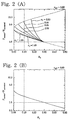
- Fig. 2(A) shows the relationship between the COD index P coated /P uncoated and the exit end reflectivity R 1 of a semiconductor laser whose exit end is coated with a high-refractive index film.
- the COD index P coated /P uncoated was calculated according to the above equations (15), (16). The calculations were carried out with respect to six different coating films having respective refractive indexes of 2.80, 2.50, 2.25, 2.00, 1.68, and 1.46, each of the six different coating films comprising a single layer.
- the coating film has a refractive index of 2.50, then the reflectivity decreases and the COD index P coated /P uncoated increases as the film thickness increases.
- the exit end reflectivity R 1 is 0.095 according to the equation (18).
- the broken-line curve in Fig. 2(A) is a curve represented by the equation (20), which indicates an upper limit for the COD index.
- Fig. 2(B) shows the relationship represented by the equation (1) by Hakki and Nash. As described above, the equation (1) by Hakki and Nash is in full agreement with the equation (19). In Fig. 2(A), the equation (1) by Hakki and Nash gives a lower limit for the COD index as indicated by the broken-line curve.
- n 1 n eff ⁇ 1- R 1 1- R 1 2 which is derived from the equations (17), (20).
- n eff 3.30
- the ideal coating film refractive index n 1 is expressed by the above equation (22), it can be understood from Fig. 2(A) that there can be obtained a semiconductor laser having a sufficient COD index even if the coating film refractive index falls in a range across the ideal coating film refractive index n 1 . If the coating film refractive index is lower than the ideal coating film refractive index, then the COD index P coated /P uncoated decreases, but the exit end reflectivity is reduced for increased oscillation efficiency. If the coating film refractive index is higher than the ideal coating film refractive index, then the exit end reflectivity increases, but the COD index P coated /P uncoated increases.
- a review of other refractive indexes shown in Fig. 2(A) with respect to the ideal coating film refractive index n 1 of 2.50 indicates that a sufficient exit end reflectivity and COD index P coated /P uncoated can be obtained by a coating film having a refractive index of 2.00, which is lower than the refractive index of 2.50 by 20 %, a coating film having a refractive index of 2.25, which is lower than the refractive index of 2.50 by 10 %, or a coating film having a refractive index of 2.80, which is higher than the refractive index of 2.50 by about 10 %.
- the coating film refractive index n 1 according to the equation (22) is not limited to the ideal value, but may be in a range of ⁇ 20 % of the ideal value, preferably, ⁇ 10 % of the ideal value.
- the coating film e.g., of TiON
- the film thickness is expressed by: ⁇ n 1 ⁇ 0.227 which is slightly smaller than ⁇ 4 n 1
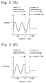
- a standing wave antinode is formed in the interface between the semiconductor and the coating film as shown in Fig. 3(B).
- the output optical density is plotted so as to be equal to the output optical density shown in Fig. 3(A).
- Fig. 4(A) shows in cross section an AlGaInP semiconductor laser according to the present invention.
- the semiconductor has a semiconductor double-heterojunction structure comprising a p-type (Al 0 . 7 Ga 0 . 3 ) 0 . 5 In 0 . 5 P cladding layer 4, an AlGaInP multiple quantum well active layer 5, and an n-type (Al 0.7 Ga 0 . 3 ) 0 . 5 In 0 . 5 P cladding layer 6.
- the AlGaInP multiple quantum well active layer 5 comprises an (Al 0 . 05 Ga 0 . 95 ) 0 . 5 In 0 .
- the semiconductor laser shown in Fig. 4(A) has an oscillation wavelength of 640 nm, and a semiconductor waveguide whose effective refractive index (n eff ) is 3.30.
- the semiconductor laser has a front exit end coated with a coating film of TiON having a refractive index of 2.50.
- a cross section of the semiconductor laser is shown in Fig. 4(B) which is taken along line IV(B) - IV(B) of Fig. 4(A).
- a GaAs block layer 10 serves to stabilize basic transverse mode oscillation.
- the GaAs block layer 10 may be replaced with either an Al 0 . 5 In 0 . 5 P block layer or an (Al x Ga 1-x ) 0 . 5 In 0 . 5 P block layer 11 shown in Fig. 4(C), where (0.5 ⁇ x ⁇ 1.0)
- the AlGaInP multiple quantum well active layer 5 may be replaced with an AlGaInP bulk active layer 12 shown in Fig. 5.
- Fig. 6(A) shows in cross section an InGaAs/AlGaAs semiconductor laser according to yet still another embodiment of the present invention.
- the InGaAs/AlGaAs semiconductor laser has an oscillation wavelength of 0.98 ⁇ m.
- a cross section of the semiconductor laser is shown in Fig. 6(B) which is taken along line VI(B) - VI(B) of Fig. 6(A).
- Fig. 7 shows in cross section an AlGaAs semiconductor laser according to a further embodiment of the present invention.
- the semiconductor laser has an oscillation wavelength of 0.83 ⁇ m.
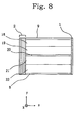
- Fig. 8 shows in cross section an InGaAlAs semiconductor laser according to a still further embodiment of the present invention.
- the InGaAlAs semiconductor laser is of a structure reported by Anan, et al., in Electronics Letters, Vol. 33, No. 12, pages 1048 - 1049, 1997.
- the semiconductor laser has an oscillation wavelength of 1.3 ⁇ m.
- the semiconductor laser has a front exit end coated with a coating film of TiON having a refractive index of 2.50 and a thickness of 120 nm.
- the high-refractive-index material for use as an exit end coating film may be any of various materials such as AlON or the like, as well as TiON. Table given below shows coating film materials that can be used in the present invention and their refractive indexes. Other materials well known as optical materials, such as CaF 2 , CeO 2 (Laser Handbook, republished 1975, page 191), or the like may also be used.
- a semiconductor laser has an effective refractive index of 3.30 and a design refractive index of 0.10, then an optimum coating film refractive index is 2.52 according to the equation (22). If the oxygen composition of TiO x N 1-x is in the range of 30 to 50 %, then an excellent coating film is produced. It is possible to control the refractive index by selecting conditions to form the film of TiO x N 1-x . If the design refractive index of the semiconductor laser is 0.05, then the optimum coating film refractive index drops to 2.28. TiO x N 1-x where the oxygen composition is large and AlO x N 1-x , SiO x N 1-x where the nitrogen composition is large are suitable for the coating film.
- Some coating film materials including TiON are highly reactive and tends to react with water vapor in the air, varying the refractive index and the transmittance of the coating film.
- the outer surface of the COD control coating film may be coated with a protective coating film for protection.
- the thickness of such a protective coating film is selected to be sufficiently large.
- the thickness of this protective coating film may be determined according to the equation: ⁇ 2 n j With the protective coating film, the optical intensity distribution in the interface between the semiconductor and the coating film as shown in FIG. 3(A) is maintained for desired operation of the semiconductor laser.
- a protective coating film for protecting the semiconductor may be interposed between the COD control coating film and the semiconductor.
- the thickness of such a protective coating film is selected to be sufficiently large.
- the thickness of this protective coating film may be determined according to the equation: ⁇ 2 n j With the protective coating film, the optical intensity distribution in the interface between the semiconductor and the coating film as shown in FIG. 3(A) is maintained for desired operation of the semiconductor laser.
- the semiconductor laser according to the present invention is capable of generating an optical output higher than the conventional limit level.
- the semiconductor laser according to the present invention can produce a high optical output even with an exit end coating film having an exit end reflectivity higher than the conventional exit end reflectivity. Consequently, the present invention provides a high-output semiconductor laser which is highly stable and reliable while keeping good oscillation characteristics such as a threshold current and temperature characteristics.
Landscapes
- Physics & Mathematics (AREA)
- Electromagnetism (AREA)
- Optics & Photonics (AREA)
- Condensed Matter Physics & Semiconductors (AREA)
- General Physics & Mathematics (AREA)
- Engineering & Computer Science (AREA)
- Plasma & Fusion (AREA)
- Semiconductor Lasers (AREA)
Applications Claiming Priority (4)
| Application Number | Priority Date | Filing Date | Title |
|---|---|---|---|
| JP34931997 | 1997-12-18 | ||
| JP34931997 | 1997-12-18 | ||
| JP12907698A JP3522107B2 (ja) | 1997-12-18 | 1998-05-12 | 半導体レーザ |
| JP12907698 | 1998-05-12 |
Publications (2)
| Publication Number | Publication Date |
|---|---|
| EP0924819A2 true EP0924819A2 (de) | 1999-06-23 |
| EP0924819A3 EP0924819A3 (de) | 2001-10-31 |
Family
ID=26464589
Family Applications (1)
| Application Number | Title | Priority Date | Filing Date |
|---|---|---|---|
| EP98123595A Withdrawn EP0924819A3 (de) | 1997-12-18 | 1998-12-10 | Halbleiterlaser und Herstellungsverfahren |
Country Status (4)
| Country | Link |
|---|---|
| US (1) | US6285700B1 (de) |
| EP (1) | EP0924819A3 (de) |
| JP (1) | JP3522107B2 (de) |
| KR (1) | KR100324147B1 (de) |
Families Citing this family (9)
| Publication number | Priority date | Publication date | Assignee | Title |
|---|---|---|---|---|
| DE10048475C2 (de) * | 2000-09-29 | 2003-04-17 | Lumics Gmbh | Passivierung der Resonatorendflächen von Halbleiterlasern auf der Basis von III-V-Halbleitermaterial |
| US20020191660A1 (en) * | 2001-05-25 | 2002-12-19 | Andreas Wittman | Anti-reflection coatings for semiconductor lasers |
| US7173953B2 (en) * | 2001-11-06 | 2007-02-06 | Bookham Technology Plc | Anti-reflection coatings for semiconductor lasers |
| DE102004024156B4 (de) * | 2004-03-31 | 2011-01-13 | Osram Opto Semiconductors Gmbh | Kantenemittierender Diodenlaser |
| JP4946243B2 (ja) * | 2005-07-29 | 2012-06-06 | 日亜化学工業株式会社 | 半導体レーザ素子、及びそれを用いた光ピックアップ装置、光学式情報再生装置 |
| JP2007201373A (ja) * | 2006-01-30 | 2007-08-09 | Sharp Corp | 半導体レーザ素子 |
| JP5233987B2 (ja) * | 2007-03-09 | 2013-07-10 | 日本電気株式会社 | 窒化物半導体レーザ |
| JP2008227169A (ja) | 2007-03-13 | 2008-09-25 | Nec Electronics Corp | 半導体レーザ素子 |
| CN119154089B (zh) * | 2024-09-09 | 2025-11-04 | 安徽格恩半导体有限公司 | 一种氮化镓基半导体激光器芯片元件 |
Family Cites Families (8)
| Publication number | Priority date | Publication date | Assignee | Title |
|---|---|---|---|---|
| US4464762A (en) * | 1982-02-22 | 1984-08-07 | Bell Telephone Laboratories, Incorporated | Monolithically integrated distributed Bragg reflector laser |
| JPH0824209B2 (ja) * | 1987-03-10 | 1996-03-06 | 古河電気工業株式会社 | 化合物半導体レ−ザ |
| EP0361399A3 (de) * | 1988-09-28 | 1990-07-18 | Canon Kabushiki Kaisha | Halbleiterlaser-Vielfachanordnung, die Laser mit Reflexionsmitteln enthält, die verschiedene Wellenlängen-Selektionseigenschaften haben |
| JPH0537085A (ja) | 1991-07-31 | 1993-02-12 | Toshiba Corp | 半導体レーザ装置 |
| US5383214A (en) * | 1992-07-16 | 1995-01-17 | Matsushita Electric Industrial Co., Ltd. | Semiconductor laser and a method for producing the same |
| JPH08307004A (ja) * | 1995-05-10 | 1996-11-22 | Oki Electric Ind Co Ltd | 半導体レーザおよびその製造方法 |
| JPH10509283A (ja) * | 1995-09-14 | 1998-09-08 | フィリップス エレクトロニクス ネムローゼ フェンノートシャップ | 半導体ダイオードレーザ及びその製造方法 |
| JPH09260777A (ja) | 1996-03-27 | 1997-10-03 | Matsushita Electric Ind Co Ltd | 半導体レーザー装置 |
-
1998
- 1998-05-12 JP JP12907698A patent/JP3522107B2/ja not_active Expired - Lifetime
- 1998-12-10 EP EP98123595A patent/EP0924819A3/de not_active Withdrawn
- 1998-12-16 US US09/212,473 patent/US6285700B1/en not_active Expired - Lifetime
- 1998-12-17 KR KR1019980055760A patent/KR100324147B1/ko not_active Expired - Fee Related
Also Published As
| Publication number | Publication date |
|---|---|
| US6285700B1 (en) | 2001-09-04 |
| KR100324147B1 (ko) | 2002-03-08 |
| KR19990063158A (ko) | 1999-07-26 |
| JPH11238940A (ja) | 1999-08-31 |
| EP0924819A3 (de) | 2001-10-31 |
| JP3522107B2 (ja) | 2004-04-26 |
Similar Documents
| Publication | Publication Date | Title |
|---|---|---|
| US5043991A (en) | Device for compensating for thermal instabilities of laser diodes | |
| US4573161A (en) | Semiconductor laser | |
| JP3856300B2 (ja) | 半導体レーザ素子 | |
| US5020066A (en) | Surface-emitting-type semiconductor laser device | |
| US6477194B1 (en) | Low temperature distributed feedback laser with loss grating and method | |
| JPH05275798A (ja) | レーザダイオード | |
| US5559818A (en) | Semiconductor laser device | |
| EP0924819A2 (de) | Halbleiterlaser und Herstellungsverfahren | |
| US7822094B2 (en) | Semiconductor laser element and method for producing same | |
| US20040233959A1 (en) | Multiple wavelength semiconductor laser and manufacturing method thereof | |
| JPS60242689A (ja) | 半導体レ−ザ素子 | |
| EP0549123B1 (de) | Halbleiterlaser mit reduzierter Temperaturabhängigkeit | |
| US7792170B2 (en) | Semiconductor laser | |
| KR100754956B1 (ko) | 반도체 레이저장치 및 레이저시스템 | |
| US20060093005A1 (en) | Semiconductor laser | |
| US6760141B2 (en) | Semiconductor optical modulator and semiconductor optical device | |
| CN100359772C (zh) | 半导体激光器 | |
| US20010021212A1 (en) | Fundamental-transverse-mode index-guided semiconductor laser device having upper optical waveguide layer thicker than lower optical waveguide layer | |
| JP2002026461A (ja) | 光半導体装置とその製造方法および光半導体装置を備えた光装置モジュール、光通信装置 | |
| JPH10303495A (ja) | 半導体レーザ | |
| JPH0358490A (ja) | 量子井戸レーザ | |
| JP2913946B2 (ja) | 量子井戸型半導体レーザ | |
| JP2001111163A (ja) | 半導体レーザ素子 | |
| JP2973612B2 (ja) | 半導体多層膜反射鏡 | |
| KR960003869B1 (ko) | 레이져 다이오드 |
Legal Events
| Date | Code | Title | Description |
|---|---|---|---|
| PUAI | Public reference made under article 153(3) epc to a published international application that has entered the european phase |
Free format text: ORIGINAL CODE: 0009012 |
|
| AK | Designated contracting states |
Kind code of ref document: A2 Designated state(s): AT BE CH CY DE DK ES FI FR GB GR IE IT LI LU MC NL PT SE Kind code of ref document: A2 Designated state(s): DE FR GB |
|
| AX | Request for extension of the european patent |
Free format text: AL;LT;LV;MK;RO;SI |
|
| PUAL | Search report despatched |
Free format text: ORIGINAL CODE: 0009013 |
|
| AK | Designated contracting states |
Kind code of ref document: A3 Designated state(s): AT BE CH CY DE DK ES FI FR GB GR IE IT LI LU MC NL PT SE |
|
| AX | Request for extension of the european patent |
Free format text: AL;LT;LV;MK;RO;SI |
|
| 17P | Request for examination filed |
Effective date: 20011030 |
|
| 17Q | First examination report despatched |
Effective date: 20020314 |
|
| AKX | Designation fees paid |
Free format text: DE FR GB |
|
| GRAH | Despatch of communication of intention to grant a patent |
Free format text: ORIGINAL CODE: EPIDOS IGRA |
|
| RIC1 | Information provided on ipc code assigned before grant |
Free format text: 7H 01S 5/028 A |
|
| RTI1 | Title (correction) |
Free format text: SEMICONDUCTOR LASER |
|
| STAA | Information on the status of an ep patent application or granted ep patent |
Free format text: STATUS: THE APPLICATION HAS BEEN WITHDRAWN |
|
| 18W | Application withdrawn |
Withdrawal date: 20021031 |