EP0924965B1 - Appareil organique électroluminescent et sa méthode de fabrication - Google Patents
Appareil organique électroluminescent et sa méthode de fabrication Download PDFInfo
- Publication number
- EP0924965B1 EP0924965B1 EP98123837A EP98123837A EP0924965B1 EP 0924965 B1 EP0924965 B1 EP 0924965B1 EP 98123837 A EP98123837 A EP 98123837A EP 98123837 A EP98123837 A EP 98123837A EP 0924965 B1 EP0924965 B1 EP 0924965B1
- Authority
- EP
- European Patent Office
- Prior art keywords
- organic layer
- barrier
- electrode
- organic electroluminescent
- predetermined pattern
- Prior art date
- Legal status (The legal status is an assumption and is not a legal conclusion. Google has not performed a legal analysis and makes no representation as to the accuracy of the status listed.)
- Expired - Lifetime
Links
Images

Classifications
-
- H—ELECTRICITY
- H05—ELECTRIC TECHNIQUES NOT OTHERWISE PROVIDED FOR
- H05B—ELECTRIC HEATING; ELECTRIC LIGHT SOURCES NOT OTHERWISE PROVIDED FOR; CIRCUIT ARRANGEMENTS FOR ELECTRIC LIGHT SOURCES, IN GENERAL
- H05B33/00—Electroluminescent light sources
- H05B33/10—Apparatus or processes specially adapted to the manufacture of electroluminescent light sources
-
- H—ELECTRICITY
- H05—ELECTRIC TECHNIQUES NOT OTHERWISE PROVIDED FOR
- H05B—ELECTRIC HEATING; ELECTRIC LIGHT SOURCES NOT OTHERWISE PROVIDED FOR; CIRCUIT ARRANGEMENTS FOR ELECTRIC LIGHT SOURCES, IN GENERAL
- H05B33/00—Electroluminescent light sources
- H05B33/12—Light sources with substantially two-dimensional [2D] radiating surfaces
- H05B33/22—Light sources with substantially two-dimensional [2D] radiating surfaces characterised by the chemical or physical composition or the arrangement of auxiliary dielectric or reflective layers
-
- H—ELECTRICITY
- H10—SEMICONDUCTOR DEVICES; ELECTRIC SOLID-STATE DEVICES NOT OTHERWISE PROVIDED FOR
- H10K—ORGANIC ELECTRIC SOLID-STATE DEVICES
- H10K50/00—Organic light-emitting devices
- H10K50/10—OLEDs or polymer light-emitting diodes [PLED]
- H10K50/11—OLEDs or polymer light-emitting diodes [PLED] characterised by the electroluminescent [EL] layers
-
- H—ELECTRICITY
- H10—SEMICONDUCTOR DEVICES; ELECTRIC SOLID-STATE DEVICES NOT OTHERWISE PROVIDED FOR
- H10K—ORGANIC ELECTRIC SOLID-STATE DEVICES
- H10K50/00—Organic light-emitting devices
- H10K50/80—Constructional details
- H10K50/805—Electrodes
- H10K50/82—Cathodes
-
- H—ELECTRICITY
- H10—SEMICONDUCTOR DEVICES; ELECTRIC SOLID-STATE DEVICES NOT OTHERWISE PROVIDED FOR
- H10K—ORGANIC ELECTRIC SOLID-STATE DEVICES
- H10K59/00—Integrated devices, or assemblies of multiple devices, comprising at least one organic light-emitting element covered by group H10K50/00
- H10K59/10—OLED displays
- H10K59/17—Passive-matrix OLED displays
- H10K59/173—Passive-matrix OLED displays comprising banks or shadow masks
-
- H—ELECTRICITY
- H10—SEMICONDUCTOR DEVICES; ELECTRIC SOLID-STATE DEVICES NOT OTHERWISE PROVIDED FOR
- H10K—ORGANIC ELECTRIC SOLID-STATE DEVICES
- H10K59/00—Integrated devices, or assemblies of multiple devices, comprising at least one organic light-emitting element covered by group H10K50/00
- H10K59/80—Constructional details
- H10K59/805—Electrodes
- H10K59/8052—Cathodes
-
- H—ELECTRICITY
- H10—SEMICONDUCTOR DEVICES; ELECTRIC SOLID-STATE DEVICES NOT OTHERWISE PROVIDED FOR
- H10K—ORGANIC ELECTRIC SOLID-STATE DEVICES
- H10K85/00—Organic materials used in the body or electrodes of devices covered by this subclass
- H10K85/10—Organic polymers or oligomers
- H10K85/141—Organic polymers or oligomers comprising aliphatic or olefinic chains, e.g. poly N-vinylcarbazol, PVC or PTFE
-
- H—ELECTRICITY
- H10—SEMICONDUCTOR DEVICES; ELECTRIC SOLID-STATE DEVICES NOT OTHERWISE PROVIDED FOR
- H10K—ORGANIC ELECTRIC SOLID-STATE DEVICES
- H10K85/00—Organic materials used in the body or electrodes of devices covered by this subclass
- H10K85/30—Coordination compounds
-
- H—ELECTRICITY
- H10—SEMICONDUCTOR DEVICES; ELECTRIC SOLID-STATE DEVICES NOT OTHERWISE PROVIDED FOR
- H10K—ORGANIC ELECTRIC SOLID-STATE DEVICES
- H10K85/00—Organic materials used in the body or electrodes of devices covered by this subclass
- H10K85/30—Coordination compounds
- H10K85/321—Metal complexes comprising a group IIIA element, e.g. Tris (8-hydroxyquinoline) gallium [Gaq3]
- H10K85/324—Metal complexes comprising a group IIIA element, e.g. Tris (8-hydroxyquinoline) gallium [Gaq3] comprising aluminium, e.g. Alq3
-
- H—ELECTRICITY
- H10—SEMICONDUCTOR DEVICES; ELECTRIC SOLID-STATE DEVICES NOT OTHERWISE PROVIDED FOR
- H10K—ORGANIC ELECTRIC SOLID-STATE DEVICES
- H10K85/00—Organic materials used in the body or electrodes of devices covered by this subclass
- H10K85/60—Organic compounds having low molecular weight
- H10K85/631—Amine compounds having at least two aryl rest on at least one amine-nitrogen atom, e.g. triphenylamine
Definitions
- the present invention relates generally to an organic electroluminescent apparatus having a plurality of organic electroluminescent devices each having an organic layer having luminescent properties provided between a hole injection electrode and an electron injection electrode in a separated state and a method of fabricating the same, which is characterized in that the plurality organic electroluminescent devices each having the organic layer having luminescent properties provided between the hole injection electrode and the electron injection electrode are simply and suitably arranged in a separated state, and particularly the plurality of organic electroluminescent devices can be suitably separated from each other even when the organic layer having luminescent properties contains a macromolecular material.
- the electroluminescent device is roughly divided into an inorganic electroluminescent device and an organic electroluminescent device depending on a used material.
- the inorganic electroluminescent device is so adapted that a high electric field is generally exerted on a luminance portion, and electrons are accelerated within the high electric field to collide with a luminescence center, whereby the luminescence center is excited to emit light.
- the organic electroluminescent device is so adapted that electrons and holes are respectively injected into a luminescent portion from an electron injection electrode and a hole injection electrode, the electrons and the holes thus injected are recombined with each other in a luminescence center to bring an organic molecule into its excited state, and the organic molecule emits fluorescence when it is returned from the excited state to its ground state.
- the inorganic electroluminescent device In the case of the inorganic electroluminescent device, a high voltage of 100 to 200 volts is required as its driving voltage because a high electric field is exerted as described above. On the other hand, the organic electroluminescent derive can be driven at a low voltage of approximately 5 to 20 volts.
- a light emitting device emitting light in a suitable color can be obtained by selecting a fluorescent material that is a luminescent material. It is expected that the organic electroluminescent device can be also utilized as a multi-color or full-color display device, for example.
- a hole injection electrode has been generally formed in a predetermined pattern on a transparent substrate such as a glass substrate and separated, and an organic layer and an electron injection electrode which are formed on the hole injection electrode have been also respectively formed in predetermined patterns and separated.
- the organic layer used for the organic electroluminescent device is generally low in heat resistance, solvent resistance, and humidity resistance.
- the organic layer and the electron injection electrode formed on the organic layer are formed in predetermined patterns by photolithography or the like, there are some problems.
- a solvent in photoresist enters the organic layer, the organic layer is dissolved in an etchant, and an organic layer is damaged by plasma at the time of dry etching.
- the organic layer and the electron injection electrode have been heretofore generally formed in predetermined patterns by evaporation using a mask member. When they are thus evaporated using the mask member, however, fine processing cannot be performed.
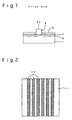
- JP-A-8-315981 and JP-A-9-102393 in providing a patterned barrier 3 on a hole injection electrode 2 formed on a transparent'substrate 1, an upper surface 3a of the barrier 3 is increased in size to provide an overhang portion, as shown in Fig. 1.
- the organic layer 4 When an organic layer 4 is evaporated from above the barrier 3. having the overhang portion thus provided by increasing the size of the upper surface 3a, the organic layer 4 is not formed under the overhang portion, so that an exposed part of the hole injection electrode 2 remains under the overhang portion.
- the electron injection electrode 5 When the electron injection electrode 5 is then evaporated, the electron injection electrode 5 may be short-circuited upon being formed on not only the organic layer 4 but also the exposed part of the hole injection electrode 2.
- the organic layer containing the macromolecular material can be generally formed simply by dipping or spin coating.
- the patterned barrier 3 is provided on the hole injection electrode 2 formed on the transparent substrate 1 as described above, however, the barrier 3 interferes with the formation. Therefore, it is difficult to form the organic layer 4 using the macromolecular material by the above-mentioned method.
- the electron injection electrode When the electron injection electrode is formed in a predetermined pattern by photolithography or the like, however, it is difficult to control etching because the thickness of the electron injection electrode is generally small. Therefore, the etchant penetrates into a portion between the organic layer containing the macromolecular material and the electron injection electrode, so that some problems occur. For example, contact characteristics between the organic layer and the electron injection electrode are degraded.
- an electrode material having a small work function such as magnesium is used as a material composing the electron injection electrode such that electrons are efficiently injected into the organic layer from the electron injection electrode, some problems occur. For example, the electron injection electrode is degraded upon being oxidized by water or the like of the etchant, so that light cannot be stably emitted.
- An object of the present invention is to make it possible to arrange, in an organic electroluminescent apparatus in which a plurality of organic electroluminescent devices each having an organic layer having luminescent properties provided between a hole injection electrode and an electron injection electrode are arranged with they being separated from one another, the electroluminescent devices in a separated state simply and suitably.
- Another object of the present invention is to make it possible to simply form, when an organic layer having luminescent properties contains a macromolecular material, the organic layer containing the macromolecular material using dipping or spin coating as well as make it possible to arrange organic electroluminescent devices in a separated state simply and suitably.
- an organic electroluminescent apparatus in arranging a plurality of organic electroluminescent devices each having an organic layer having luminescent properties provided between a first electrode and a second electrode in a separated state, a barrier having electrical insulating properties is formed in a predetermined pattern on the organic layer, to separate the organic electroluminescent devices from each other by the barrier.
- An example of such an organic electroluminescent apparatus is one comprising a first electrode formed in a predetermined pattern on a substrate, an organic layer having luminescent properties provided on the first electrode, a barrier having electrical insulating properties formed in a predetermined pattern on the organic layer, and a second electrode formed on the organic layer upon being separated by the barrier having electrical insulating properties.
- a method of fabricating an organic electroluminescent apparatus comprises the steps of providing a first electrode in a predetermined pattern on a substrate, providing an organic layer having luminescent properties on the first electrode, providing a barrier having electrical insulating properties with a predetermined pattern on the organic layer, and providing a second electrode separated by the barrier having electrical insulating properties on the organic layer.
- the first electrode with a predetermined pattern is formed on the substrate, the organic layer having luminescent properties is provided on the substrate having the first electrode formed thereon, the barrier having electrical insulating properties with a predetermined pattern is provided on the organic layer, and the electron injection electrode is provided from above the barrier having electrical insulating properties. Consequently, the electron injection electrode is separated by the barrier, so that the organic electroluminescent devices are arranged in a separated state.
- the barrier having electrical insulating properties is provided on the organic layer. Even when the upper surface of the barrier is increased in size to provide an overhang portion, the first electrode is not exposed under the overhang portion. When the second electrode is formed, the second electrode and the first electrode are not short-circuited upon being brought into contact with each other.
- the organic layer is formed, and the barrier is then provided on the organic layer.
- the organic layer is formed by painting the substrate having the first electrode formed thereon with a macromolecular material solution by the method of dipping or spin coating, therefore, the barrier does not interfere with the formation.
- macromolecular materials used for the organic layer include macromolecular materials having fluorescent properties such as a poly(p-phenylene vinylene) derivative, polythiophene, and polyvinyl carbazole, and macromolecular materials having electrical insulating properties, in which a pigment is doped, such as polymethyl methacrylate and polycarbonate.
- the barrier having electrically insulating properties on the organic layer when a macromolecular material solution for barrier formation is applied, the applied macromolecular material solution for barrier formation is solidified, and the barrier having electrically insulating properties with a predetermined pattern is then formed by etching, used as the macromolecular material in the organic layer is one which is insoluble in the macromolecular material solution for barrier formation or an etchant.
- the barrier having electrical insulation properties with a predetermined pattern when the barrier having electrical insulation properties with a predetermined pattern is provided on the organic layer, and an electrode material is evaporated from above the barrier having electrical insulating properties, to provide a second electrode on the organic layer separated by the barrier having electrical insulating properties, the second electrode formed on the organic layer need not be formed in a predetermined pattern upon being processed by an etchant. Therefore, the possibilities that the etchant penetrates into a portion between the organic layer and the second electrode as in the conventional example, so that contact properties between the organic layer and the second electrode are degraded, and the second electrode is degraded upon being oxidized are eliminated, so that light can be stably emitted in each of the organic electroluminescent devices.
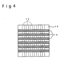
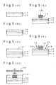
- a plurality of columns of transparent hole injection electrodes 12 each composed of an indium-tin oxide (ITO) were provided with required spacing using a normal resist process on a transparent substrate 11 composed of glass, as shown in Figs. 2 and 3 (A).
- ITO indium-tin oxide
- polymethyl methacrylate indicated by the following chemical formula 3 were dissolved in dichloromethane.
- a solution thus obtained was applied onto the transparent substrate 11 having the plurality of columns of hole injection electrodes 12 formed thereon as described above using spin coating, and was then solidified upon being heated at a temperature of 120°C, to form an organic layer 13 using a macromolecular material on the transparent substrate 11 having the hole injection electrodes 12 formed thereon.
- Positive resist 14' (Tokyo Ohka Kogyo K.K.: OFPR-1000) was applied so as to have a thickness of 1.5 ⁇ m, as shown in Fig. 3 (C), to the organic layer 13 containing a macromolecular material as described above, was heat-treated, and was then exposed in a predetermined pattern using a photomask 20, as shown in Fig. 3 (D), in accordance with normal photolithography in the positive resist 14'.
- etching was made in such a manner that a part, which has not been exposed, of the positive resist 14' would remain, to provide a plurality of rows of barriers 14 each having an overhang portion provided by increasing the size of its upper surface 14a on the organic layer 13 so as to be perpendicular to the hole injection electrodes 12, as shown in Figs. 3(E) and 4.
- An electron injection electrode 15 composed of an Al - Li alloy was formed by vacuum evaporation, as shown in Fig. 3 (F), on the organic layer 13 having the plurality of rows of barriers 14 thus provided thereon, and the electron injection electrode 15 was separated by the barriers 14, to obtain an organic electroluminescent apparatus having s plurality of organic electroluminescent devices 10 arranged thereon in a matrix.
- the organic electroluminescent apparatus In the organic electroluminescent apparatus according to the embodiment 1, consider a case where a voltage is applied between the hole injection electrodes 12 and the electron injection electrodes 15. In this case, when the voltage was 17 volts, green light having luminance of 1000 cd/cm 2 could be emitted from each of the organic electroluminescent devices 10. Further, the organic electroluminescent devices 10 were suitably separated from each other, so that no short also occurred.
- a plurality of columns of transparent hole injection electrodes 12 each composed of ITO were provided with required spacing on a transparent substrate 11 composed of glass, after which poly(p-phenylene vinylene) (PPV) was formed as an organic layer 13 using a macromolecular material.
- the organic layer 13 composed of PPV was formed in accordance with a method described in a document [J. H. Burroughes, et al, Nature, Vol. 347, pp.539-541 (1990)].
- a plurality of rows of barriers 14 each having an overhang portion by increasing the size of its upper surface 14a were provided on the organic layer 13 so as to be perpendicular to the hole injection electrodes 12, an electron injection electrode 15 composed of an Al - Li alloy was formed on the organic layer 13 having the barriers 14 thus provided thereon by vacuum evaporation, and the electron injection electrode 15 was separated by the barriers 14, to obtain an organic electroluminescent apparatus having a plurality of organic electroluminescent devices 10 arranged thereon in a matrix.
- the organic layer 13 composed of PPV was not dissolved in a solution of the above-mentioned positive resist 14' (produced by Tokyo Ohka Kogyo K.K.: OFPR - 1000) or an etchant.
- the organic electroluminescent apparatus consider a case where a voltage is applied between the hole injection electrodes 12 and the electron injection electrodes 15. In this case, when the voltage was 15 volts, yellow green light having luminance of 100 cd/m 2 could be emitted from each of the organic electroluminescent devices 10. Further, the organic electroluminescent devices 10 were suitably separated from each other, so that no short also occurred.
- an organic electroluminescent apparatus was fabricated in the same manner as the organic electroluminescent apparatus according to the above-mentioned embodiment 1 except that in providing an organic layer 13, polycarbonate was used in place of the above-mentioned polymethyl methacrylate.
- organic electroluminescent apparatus In the organic electroluminescent apparatus according to the embodiment 3, consider a case where a voltage is applied between hole injection electrodes 12 and electron injection electrodes 15. In this case, when the voltage was 15 volts, green light having luminance of 1200 cd/m 2 could be emitted from each of organic electroluminescent devices 10. Further, the organic electroluminescent devices 10 were suitably separated from each other, so that no short also occurred.
- a plurality of columns of transparent hole injection electrodes 12 each composed of ITO were provided with required spacing on a transparent substrate 11 composed of glass in the same manner as that in the above-mentioned embodiment 1, and an organic layer 13 containing the same macromolecular material as that in the embodiment 1 was provided thereon, as shown in Figs. 5 (A) and 5 (B).
- negative resist 14" produced by Nippon Zeon K.K. was used in place of the above-mentioned positive resist 14' (produced by Tokyo Ohka Kogyo K.K.: OFPR - 1000), as shown in Fig. 5 (C).
- the negative resist 14" was exposed in a predetermined pattern using a photomask 20, as shown in Fig. 5 (D), in accordance with normal photolithography in the negative resist 14".
- the barriers 14 were provided using the negative resist 14" as in the embodiment 4, it was possible to set the height of the barriers 14 to 5 ⁇ m.
- the electron injection electrodes 15 could be more reliably separated from each other by the barriers 14, so that the organic electroluminescent devices 10 could be reliably separated from each other. Therefore, the yield of the electroluminescent apparatus is improved by approximately 30 %.
- the transparent hole injection electrodes composed of ITO are provided on the transparent substrate, the transparent hole injection electrodes composed of ITO can be also provided on the organic layer after being separated from each other by barriers.
Landscapes
- Physics & Mathematics (AREA)
- Optics & Photonics (AREA)
- Engineering & Computer Science (AREA)
- Manufacturing & Machinery (AREA)
- Electroluminescent Light Sources (AREA)
Claims (16)
- Appareil électroluminescent organique réalisé en disposant plusieurs dispositifs électroluminescents organiques comportant chacun une couche organique à propriétés luminescentes réalisée entre une première électrode et une seconde électrode dans un état séparé,
une barrière à propriétés électriquement isolantes étant formée suivant un motif préfixé sur la couche organique, afin de séparer les dispositifs électroluminescents organiques entre eux au moyen de la barrière. - Appareil électroluminescent organique suivant la revendication 1, dans lequel
la première électrode est formée suivant un motif préfixé sur un substrat,
la couche organique à propriétés luminescentes est réalisée sur la première électrode,
la barrière à propriétés électriquement isolantes est formée suivant un motif préfixé sur la couche organique, et
la seconde électrode est formée sur la couche organique en étant séparée par la barrière à propriétés électriquement isolantes. - Appareil électroluminescent organique suivant la revendication 1, dans lequel
la couche organique à propriétés luminescentes contient une matière macromoléculaire. - Appareil électroluminescent organique suivant la revendication 1, dans lequel
la couche organique possède une résistance aux solvants. - Appareil électroluminescent organique suivant la revendication 2, dans lequel
la première électrode formée suivant un motif préfixé et la barrière à propriétés électriquement isolantes formée suivant un motif préfixé se croisent l'une l'autre. - Procédé de fabrication d'un appareil électroluminescent organique, comprenant les opérations consistant :à réaliser une première électrode suivant un motif préfixé sur un substrat ;à réaliser une couche organique à propriétés luminescentes sur la première électrode ;à réaliser une barrière à propriétés électriquement isolantes suivant un motif préfixé sur la couche organique ; età réaliser une seconde électrode séparée par la barrière à propriétés électriquement isolantes sur la couche organique.
- Procédé suivant la revendication 6, selon lequel
la première électrode à motif préfixé et la barrière à propriétés électriquement isolantes à motif préfixé sont réalisées de façon à se croiser l'une l'autre. - Procédé suivant la revendication 6, selon lequel
la couche organique à propriétés luminescentes contient une matière macromoléculaire. - Procédé suivant la revendication 6, selon lequel
la couche organique est formée en appliquant une solution de matière macromoléculaire au substrat sur lequel la première électrode est formée et à soumettre la solution à un traitement de recuisson. - Procédé suivant la revendication 9, selon lequel
une méthode d'application de la solution de matière macromoléculaire au substrat sur lequel la première électrode est formée est un revêtement centrifuges ou une immersion. - Procédé suivant la revendication 6, selon lequel
la barrière à propriétés électriquement isolantes à motif préfixé est réalisée sur la couche organique par photolithographie. - Procédé suivant la revendication 6, selon lequel
une matière d'électrodes est appliquée sous forme vapeur à partir d'au-dessus de la barrière ayant des propriétés électriquement isolantes, afin de réaliser une seconde électrode séparée par la barrière à propriétés électriquement isolantes sur la couche organique. - Procédé suivant la revendication 6, selon lequel
la barrière à propriétés électriquement isolantes contient une matière macromoléculaire. - Procédé suivant la revendication 13, selon lequel
la matière macromoléculaire composant la barrière est une matière de réserve. - Procédé suivant la revendication 9, selon lequel
une solution de matière macromoléculaire pour formation de barrière est appliquée à la couche organique formée par le traitement de recuisson et la solution est soumise à un traitement de recuit, afin de former une barrière à propriétés électriquement isolantes suivant un motif préfixé. - Procédé suivant la revendication 15, selon lequel
la matière macromoléculaire composant la couche organique est dissoute dans la solution de matière macromoléculaire pour formation de barrière.
Applications Claiming Priority (2)
| Application Number | Priority Date | Filing Date | Title |
|---|---|---|---|
| JP34765697 | 1997-12-17 | ||
| JP34765697A JP3540584B2 (ja) | 1997-12-17 | 1997-12-17 | 有機エレクトロルミネッセンス装置及びその製造方法 |
Publications (2)
| Publication Number | Publication Date |
|---|---|
| EP0924965A1 EP0924965A1 (fr) | 1999-06-23 |
| EP0924965B1 true EP0924965B1 (fr) | 2002-05-22 |
Family
ID=18391703
Family Applications (1)
| Application Number | Title | Priority Date | Filing Date |
|---|---|---|---|
| EP98123837A Expired - Lifetime EP0924965B1 (fr) | 1997-12-17 | 1998-12-15 | Appareil organique électroluminescent et sa méthode de fabrication |
Country Status (4)
| Country | Link |
|---|---|
| US (2) | US6232713B1 (fr) |
| EP (1) | EP0924965B1 (fr) |
| JP (1) | JP3540584B2 (fr) |
| DE (1) | DE69805490T2 (fr) |
Families Citing this family (15)
| Publication number | Priority date | Publication date | Assignee | Title |
|---|---|---|---|---|
| JP3807114B2 (ja) * | 1998-08-25 | 2006-08-09 | カシオ計算機株式会社 | 発光素子の製造方法 |
| US6936485B2 (en) * | 2000-03-27 | 2005-08-30 | Semiconductor Energy Laboratory Co., Ltd. | Method of manufacturing a light emitting device |
| KR100570991B1 (ko) * | 2000-12-20 | 2006-04-13 | 삼성에스디아이 주식회사 | 유기 전계 발광 소자 판넬의 제작 방법 |
| US6893887B2 (en) * | 2001-01-18 | 2005-05-17 | Semiconductor Energy Laboratory Co., Ltd. | Process for producing a light emitting device |
| US20040106005A1 (en) * | 2001-02-20 | 2004-06-03 | Yuji Hamada | Luminescent element |
| EP1388171A1 (fr) * | 2001-05-03 | 2004-02-11 | Koninklijke Philips Electronics N.V. | Dispositif electroluminescent |
| KR100723011B1 (ko) * | 2001-05-28 | 2007-05-29 | 주식회사 동진쎄미켐 | 보조 전극을 갖는 유기 전기발광 디스플레이의 제조 방법 |
| JP4578032B2 (ja) * | 2001-08-22 | 2010-11-10 | 大日本印刷株式会社 | エレクトロルミネッセント素子の製造方法 |
| JP2003217855A (ja) * | 2002-01-28 | 2003-07-31 | Matsushita Electric Ind Co Ltd | エレクトロルミネッセンス表示装置及びその製造方法 |
| EP1369499A3 (fr) * | 2002-04-15 | 2004-10-20 | Semiconductor Energy Laboratory Co., Ltd. | Méthode et appareillage pour fabriquer un dispositif émetteur de lumière |
| TWI232695B (en) * | 2002-09-17 | 2005-05-11 | Ibm | Organic light emitting diode device and method for manufacturing the organic light emitting diode device |
| JP4299059B2 (ja) * | 2003-05-30 | 2009-07-22 | 株式会社 日立ディスプレイズ | 有機エレクトロルミネッセンス表示装置の製造方法 |
| US20110284889A1 (en) * | 2009-01-21 | 2011-11-24 | Tohoku Pioneer Corporation | Organic el panel and method for manufacturing the same |
| JP5113865B2 (ja) * | 2010-03-11 | 2013-01-09 | 株式会社東芝 | 有機エレクトロルミネッセンス表示装置の製造方法 |
| WO2015000095A1 (fr) | 2013-07-05 | 2015-01-08 | Industrial Technology Research Institute | Écran souple et son procédé de fabrication |
Family Cites Families (9)
| Publication number | Priority date | Publication date | Assignee | Title |
|---|---|---|---|---|
| US5276380A (en) * | 1991-12-30 | 1994-01-04 | Eastman Kodak Company | Organic electroluminescent image display device |
| JPH07220871A (ja) * | 1994-01-28 | 1995-08-18 | Res Dev Corp Of Japan | 有機エレクトロルミネッセンスデバイス |
| JP3813217B2 (ja) | 1995-03-13 | 2006-08-23 | パイオニア株式会社 | 有機エレクトロルミネッセンスディスプレイパネルの製造方法 |
| JP3208638B2 (ja) | 1995-01-31 | 2001-09-17 | 双葉電子工業株式会社 | 有機エレクトロルミネセント表示装置およびその製造方法 |
| JP3401356B2 (ja) | 1995-02-21 | 2003-04-28 | パイオニア株式会社 | 有機エレクトロルミネッセンスディスプレイパネルとその製造方法 |
| JP4142117B2 (ja) | 1995-10-06 | 2008-08-27 | パイオニア株式会社 | 有機エレクトロルミネッセンスディスプレイパネル及びその製造方法 |
| JPH09298090A (ja) * | 1996-04-30 | 1997-11-18 | Hokuriku Electric Ind Co Ltd | El素子とその製造方法及びその駆動方法 |
| JP2815004B2 (ja) * | 1996-10-30 | 1998-10-27 | 日本電気株式会社 | 表示装置およびその製造方法 |
| JP3485749B2 (ja) * | 1997-02-17 | 2004-01-13 | 三洋電機株式会社 | 有機エレクトロルミネッセンス表示装置 |
-
1997
- 1997-12-17 JP JP34765697A patent/JP3540584B2/ja not_active Expired - Fee Related
-
1998
- 1998-12-15 EP EP98123837A patent/EP0924965B1/fr not_active Expired - Lifetime
- 1998-12-15 DE DE69805490T patent/DE69805490T2/de not_active Expired - Fee Related
- 1998-12-15 US US09/211,041 patent/US6232713B1/en not_active Expired - Lifetime
-
2001
- 2001-02-26 US US09/791,833 patent/US6352462B2/en not_active Expired - Fee Related
Also Published As
| Publication number | Publication date |
|---|---|
| EP0924965A1 (fr) | 1999-06-23 |
| US6232713B1 (en) | 2001-05-15 |
| DE69805490D1 (de) | 2002-06-27 |
| US6352462B2 (en) | 2002-03-05 |
| JPH11185968A (ja) | 1999-07-09 |
| DE69805490T2 (de) | 2003-01-16 |
| US20010009350A1 (en) | 2001-07-26 |
| JP3540584B2 (ja) | 2004-07-07 |
Similar Documents
| Publication | Publication Date | Title |
|---|---|---|
| EP0924965B1 (fr) | Appareil organique électroluminescent et sa méthode de fabrication | |
| JP4684378B2 (ja) | 有機elディスプレイパネルの製造方法 | |
| US6091196A (en) | Organic electroluminescent display device and method of manufacture thereof | |
| KR100267964B1 (ko) | 유기 이엘(el) 디스플레이 패널 및 그 제조 방법 | |
| EP0951073A2 (fr) | Procédé de fabrication de dispositifs organiques polymères électroluminescents à pixels | |
| JP2002324672A (ja) | 有機伝導性物質のマトリックス配列の形成方法及びこれにより製造されたマトリックス配列 | |
| CN103035852A (zh) | 发光装置的制造方法 | |
| JP2000235891A (ja) | 有機電界発光装置 | |
| JP2002025781A (ja) | 有機el素子およびその製造方法 | |
| JP2004535045A (ja) | 有機エレクトロルミネセンスディスプレー及びその製造 | |
| US6614177B2 (en) | Organic light emitting device and method of manufacturing the same | |
| JP2003203769A (ja) | 線状パターン及びパターン形成方法、画像表示装置及びその製造方法 | |
| WO2003092333A1 (fr) | Procede pour fabriquer un element el organique | |
| JP3369867B2 (ja) | 有機エレクトロルミネッセンスパネル | |
| JP4774787B2 (ja) | 表示装置 | |
| JP2002246173A (ja) | 有機elデバイスおよびこの製造方法 | |
| JP2002151255A (ja) | 有機エレクトロルミネッセンスディスプレイパネル及びその製造方法 | |
| JP4310866B2 (ja) | 有機エレクトロルミネッセンス表示素子用基板及び表示素子 | |
| JP2000200680A (ja) | 有機電界発光素子の製造方法 | |
| JPH11191489A (ja) | 有機電界発光装置 | |
| KR102577783B1 (ko) | 광 전자 소자의 제조 방법 | |
| JP4044362B2 (ja) | 有機el素子の製造方法 | |
| KR100351822B1 (ko) | 유기 el 소자의 제조방법 | |
| JPH08171989A (ja) | エレクトロルミネセンス発光素子 | |
| KR100277641B1 (ko) | 유기 전자발광소자 |
Legal Events
| Date | Code | Title | Description |
|---|---|---|---|
| PUAI | Public reference made under article 153(3) epc to a published international application that has entered the european phase |
Free format text: ORIGINAL CODE: 0009012 |
|
| AK | Designated contracting states |
Kind code of ref document: A1 Designated state(s): DE FR GB |
|
| AX | Request for extension of the european patent |
Free format text: AL;LT;LV;MK;RO;SI |
|
| 17P | Request for examination filed |
Effective date: 19991103 |
|
| AKX | Designation fees paid |
Free format text: DE FR GB |
|
| GRAG | Despatch of communication of intention to grant |
Free format text: ORIGINAL CODE: EPIDOS AGRA |
|
| 17Q | First examination report despatched |
Effective date: 20010625 |
|
| GRAG | Despatch of communication of intention to grant |
Free format text: ORIGINAL CODE: EPIDOS AGRA |
|
| GRAH | Despatch of communication of intention to grant a patent |
Free format text: ORIGINAL CODE: EPIDOS IGRA |
|
| GRAH | Despatch of communication of intention to grant a patent |
Free format text: ORIGINAL CODE: EPIDOS IGRA |
|
| GRAA | (expected) grant |
Free format text: ORIGINAL CODE: 0009210 |
|
| REG | Reference to a national code |
Ref country code: GB Ref legal event code: FG4D |
|
| REF | Corresponds to: |
Ref document number: 69805490 Country of ref document: DE Date of ref document: 20020627 |
|
| ET | Fr: translation filed | ||
| PLBE | No opposition filed within time limit |
Free format text: ORIGINAL CODE: 0009261 |
|
| STAA | Information on the status of an ep patent application or granted ep patent |
Free format text: STATUS: NO OPPOSITION FILED WITHIN TIME LIMIT |
|
| 26N | No opposition filed |
Effective date: 20030225 |
|
| GBPC | Gb: european patent ceased through non-payment of renewal fee |
Effective date: 20031215 |
|
| REG | Reference to a national code |
Ref country code: GB Ref legal event code: 728V |
|
| REG | Reference to a national code |
Ref country code: GB Ref legal event code: 728Y |
|
| PGFP | Annual fee paid to national office [announced via postgrant information from national office to epo] |
Ref country code: FR Payment date: 20081212 Year of fee payment: 11 |
|
| PGFP | Annual fee paid to national office [announced via postgrant information from national office to epo] |
Ref country code: DE Payment date: 20081211 Year of fee payment: 11 |
|
| PGFP | Annual fee paid to national office [announced via postgrant information from national office to epo] |
Ref country code: GB Payment date: 20081210 Year of fee payment: 11 |
|
| GBPC | Gb: european patent ceased through non-payment of renewal fee |
Effective date: 20091215 |
|
| REG | Reference to a national code |
Ref country code: FR Ref legal event code: ST Effective date: 20100831 |
|
| PG25 | Lapsed in a contracting state [announced via postgrant information from national office to epo] |
Ref country code: FR Free format text: LAPSE BECAUSE OF NON-PAYMENT OF DUE FEES Effective date: 20091231 |
|
| PG25 | Lapsed in a contracting state [announced via postgrant information from national office to epo] |
Ref country code: DE Free format text: LAPSE BECAUSE OF NON-PAYMENT OF DUE FEES Effective date: 20100701 |
|
| PG25 | Lapsed in a contracting state [announced via postgrant information from national office to epo] |
Ref country code: GB Free format text: LAPSE BECAUSE OF NON-PAYMENT OF DUE FEES Effective date: 20091215 |