EP0925932A2 - Druckkopfspannungsentlastung - Google Patents
Druckkopfspannungsentlastung Download PDFInfo
- Publication number
- EP0925932A2 EP0925932A2 EP98310285A EP98310285A EP0925932A2 EP 0925932 A2 EP0925932 A2 EP 0925932A2 EP 98310285 A EP98310285 A EP 98310285A EP 98310285 A EP98310285 A EP 98310285A EP 0925932 A2 EP0925932 A2 EP 0925932A2
- Authority
- EP
- European Patent Office
- Prior art keywords
- polymeric layer
- ink
- printhead
- valleys
- polymeric
- Prior art date
- Legal status (The legal status is an assumption and is not a legal conclusion. Google has not performed a legal analysis and makes no representation as to the accuracy of the status listed.)
- Granted
Links
Images

Classifications
-
- B—PERFORMING OPERATIONS; TRANSPORTING
- B41—PRINTING; LINING MACHINES; TYPEWRITERS; STAMPS
- B41J—TYPEWRITERS; SELECTIVE PRINTING MECHANISMS, i.e. MECHANISMS PRINTING OTHERWISE THAN FROM A FORME; CORRECTION OF TYPOGRAPHICAL ERRORS
- B41J2/00—Typewriters or selective printing mechanisms characterised by the printing or marking process for which they are designed
- B41J2/005—Typewriters or selective printing mechanisms characterised by the printing or marking process for which they are designed characterised by bringing liquid or particles selectively into contact with a printing material
- B41J2/01—Ink jet
- B41J2/135—Nozzles
- B41J2/16—Production of nozzles
- B41J2/1621—Manufacturing processes
- B41J2/1631—Manufacturing processes photolithography
-
- B—PERFORMING OPERATIONS; TRANSPORTING
- B41—PRINTING; LINING MACHINES; TYPEWRITERS; STAMPS
- B41J—TYPEWRITERS; SELECTIVE PRINTING MECHANISMS, i.e. MECHANISMS PRINTING OTHERWISE THAN FROM A FORME; CORRECTION OF TYPOGRAPHICAL ERRORS
- B41J2/00—Typewriters or selective printing mechanisms characterised by the printing or marking process for which they are designed
- B41J2/005—Typewriters or selective printing mechanisms characterised by the printing or marking process for which they are designed characterised by bringing liquid or particles selectively into contact with a printing material
- B41J2/01—Ink jet
- B41J2/135—Nozzles
- B41J2/14—Structure thereof only for on-demand ink jet heads
- B41J2/14016—Structure of bubble jet print heads
- B41J2/14032—Structure of the pressure chamber
-
- B—PERFORMING OPERATIONS; TRANSPORTING
- B41—PRINTING; LINING MACHINES; TYPEWRITERS; STAMPS
- B41J—TYPEWRITERS; SELECTIVE PRINTING MECHANISMS, i.e. MECHANISMS PRINTING OTHERWISE THAN FROM A FORME; CORRECTION OF TYPOGRAPHICAL ERRORS
- B41J2/00—Typewriters or selective printing mechanisms characterised by the printing or marking process for which they are designed
- B41J2/005—Typewriters or selective printing mechanisms characterised by the printing or marking process for which they are designed characterised by bringing liquid or particles selectively into contact with a printing material
- B41J2/01—Ink jet
- B41J2/135—Nozzles
- B41J2/16—Production of nozzles
- B41J2/1601—Production of bubble jet print heads
-
- B—PERFORMING OPERATIONS; TRANSPORTING
- B41—PRINTING; LINING MACHINES; TYPEWRITERS; STAMPS
- B41J—TYPEWRITERS; SELECTIVE PRINTING MECHANISMS, i.e. MECHANISMS PRINTING OTHERWISE THAN FROM A FORME; CORRECTION OF TYPOGRAPHICAL ERRORS
- B41J2/00—Typewriters or selective printing mechanisms characterised by the printing or marking process for which they are designed
- B41J2/005—Typewriters or selective printing mechanisms characterised by the printing or marking process for which they are designed characterised by bringing liquid or particles selectively into contact with a printing material
- B41J2/01—Ink jet
- B41J2/135—Nozzles
- B41J2/16—Production of nozzles
- B41J2/162—Manufacturing of the nozzle plates
-
- B—PERFORMING OPERATIONS; TRANSPORTING
- B41—PRINTING; LINING MACHINES; TYPEWRITERS; STAMPS
- B41J—TYPEWRITERS; SELECTIVE PRINTING MECHANISMS, i.e. MECHANISMS PRINTING OTHERWISE THAN FROM A FORME; CORRECTION OF TYPOGRAPHICAL ERRORS
- B41J2/00—Typewriters or selective printing mechanisms characterised by the printing or marking process for which they are designed
- B41J2/005—Typewriters or selective printing mechanisms characterised by the printing or marking process for which they are designed characterised by bringing liquid or particles selectively into contact with a printing material
- B41J2/01—Ink jet
- B41J2/135—Nozzles
- B41J2/16—Production of nozzles
- B41J2/1621—Manufacturing processes
- B41J2/1623—Manufacturing processes bonding and adhesion
-
- B—PERFORMING OPERATIONS; TRANSPORTING
- B41—PRINTING; LINING MACHINES; TYPEWRITERS; STAMPS
- B41J—TYPEWRITERS; SELECTIVE PRINTING MECHANISMS, i.e. MECHANISMS PRINTING OTHERWISE THAN FROM A FORME; CORRECTION OF TYPOGRAPHICAL ERRORS
- B41J2/00—Typewriters or selective printing mechanisms characterised by the printing or marking process for which they are designed
- B41J2/005—Typewriters or selective printing mechanisms characterised by the printing or marking process for which they are designed characterised by bringing liquid or particles selectively into contact with a printing material
- B41J2/01—Ink jet
- B41J2/135—Nozzles
- B41J2/16—Production of nozzles
- B41J2/1621—Manufacturing processes
- B41J2/1626—Manufacturing processes etching
-
- B—PERFORMING OPERATIONS; TRANSPORTING
- B41—PRINTING; LINING MACHINES; TYPEWRITERS; STAMPS
- B41J—TYPEWRITERS; SELECTIVE PRINTING MECHANISMS, i.e. MECHANISMS PRINTING OTHERWISE THAN FROM A FORME; CORRECTION OF TYPOGRAPHICAL ERRORS
- B41J2/00—Typewriters or selective printing mechanisms characterised by the printing or marking process for which they are designed
- B41J2/005—Typewriters or selective printing mechanisms characterised by the printing or marking process for which they are designed characterised by bringing liquid or particles selectively into contact with a printing material
- B41J2/01—Ink jet
- B41J2/135—Nozzles
- B41J2/16—Production of nozzles
- B41J2/1621—Manufacturing processes
- B41J2/1632—Manufacturing processes machining
- B41J2/1634—Manufacturing processes machining laser machining
-
- B—PERFORMING OPERATIONS; TRANSPORTING
- B41—PRINTING; LINING MACHINES; TYPEWRITERS; STAMPS
- B41J—TYPEWRITERS; SELECTIVE PRINTING MECHANISMS, i.e. MECHANISMS PRINTING OTHERWISE THAN FROM A FORME; CORRECTION OF TYPOGRAPHICAL ERRORS
- B41J2/00—Typewriters or selective printing mechanisms characterised by the printing or marking process for which they are designed
- B41J2/005—Typewriters or selective printing mechanisms characterised by the printing or marking process for which they are designed characterised by bringing liquid or particles selectively into contact with a printing material
- B41J2/01—Ink jet
- B41J2/135—Nozzles
- B41J2/16—Production of nozzles
- B41J2/1621—Manufacturing processes
- B41J2/1635—Manufacturing processes dividing the wafer into individual chips
-
- B—PERFORMING OPERATIONS; TRANSPORTING
- B41—PRINTING; LINING MACHINES; TYPEWRITERS; STAMPS
- B41J—TYPEWRITERS; SELECTIVE PRINTING MECHANISMS, i.e. MECHANISMS PRINTING OTHERWISE THAN FROM A FORME; CORRECTION OF TYPOGRAPHICAL ERRORS
- B41J2/00—Typewriters or selective printing mechanisms characterised by the printing or marking process for which they are designed
- B41J2/005—Typewriters or selective printing mechanisms characterised by the printing or marking process for which they are designed characterised by bringing liquid or particles selectively into contact with a printing material
- B41J2/01—Ink jet
- B41J2/135—Nozzles
- B41J2/16—Production of nozzles
- B41J2/1621—Manufacturing processes
- B41J2/164—Manufacturing processes thin film formation
- B41J2/1645—Manufacturing processes thin film formation thin film formation by spincoating
Definitions
- the invention relates to an improved printhead design for an ink jet printer and to a method for reducing thermal and/or mechanical stress in a composite printhead structure.
- Ink jet printheads are composite structures which are conventionally made by bonding a metal or plastic nozzle plate to a semiconductor substrate either directly using an adhesive or by bonding the nozzle plate to a polymeric layer which is deposited on or bonded to the substrate.
- the polymeric layer may be patterned before or after bonding to the substrate in order to provide ink flow features which provide ink to the regions of the printhead which induce the ink to be expelled through the nozzle plate to a print media.
- An object of the invention is to improve component alignment in a printhead structure.
- Another object of the invention is to reduce thermal stresses in print head components during assembly thereof.
- a further object of the invention is to provide a less costly manufacturing process for printhead components which induces relatively less thermal stresses in the components parts thereof.
- the invention provides a printhead composite structure including a semiconductor substrate containing energy imparting devices for ink and electrical tracing connected thereto on a surface of the substrate, a thick film polymeric layer adjacent the energy imparting surface of the substrate and a nozzle plate attached to the polymeric layer.
- the polymeric layer has a sufficient thickness and size suitable for containing a plurality of ink chambers and ink flow channels and a plurality of valleys in an area of the polymeric layer adjacent the ink chambers which valleys are sufficient to inhibit thermally induced stresses in the polymeric layer during a process for bonding the nozzle plate to the polymeric layer.
- the invention provides a method for making an ink jet printhead which comprises providing a semiconductor substrate containing electrical tracing connected to energy imparting devices for ink on a surface of the substrate, applying a polymeric layer onto the surface of the semiconductor substrate, the polymeric layer having a thickness ranging from about 2 to about 50 microns, preferably from about 10 to about 30 microns, treating the polymeric layer in one or more steps to provide ink chambers and ink flow channels therein for flow of ink to the energy imparting devices and to produce valleys adjacent the ink chambers, and bonding a metal coated nozzle plate adjacent to the polymeric layer using heat thereby forming an ink jet printhead, wherein the valleys are of a size and located in an area of the polymeric layer sufficient to minimize thermal stresses in the polymeric layer during the bonding process.
- the invention provides thermal ink jet printer cartridge which comprises an ink reservoir body, electrical contacts for connecting the cartridge to a printer and a printhead structure attached to an electrical tab circuit containing the contacts, wherein the printhead structure comprises a semiconductor substrate having thermal resistance elements and electrical traces on a ink wettable surface thereof and an ink via therethrough, a photoresist thick film polymeric layer attached adjacent the ink wettable surface of the substrate and a metal, metal coated or plastic nozzle plate attached to the polymeric layer wherein the polymeric layer contains a multiplicity of ink flow channels leading from an inlet ink region to ink chambers adjacent the inlet ink region.
- the polymeric layer also contains a plurality of voids in an area of the polymeric layer adjacent the ink chambers, the voids having a size sufficient to inhibit thermal stresses in the printhead structure during a manufacturing process therefor.
- An advantage of the invention is that the valleys or voids, which provide reduced thermal stresses during the process of bonding the nozzle plate to the polymeric layer, are formed in the polymeric layer rather than in the nozzle plate thereby simplifying the manufacturing process. Furthermore, the valleys or voids may be produced at the same time or substantially the same time as the production of other flow features in the thick film or polymeric layer thereby reducing the number of process steps as compared to producing a metal or metal coated nozzle plate and forming the valleys or voids in the nozzle plate using a separate machining step.
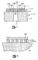
- Fig. 1 is a cross-sectional view from one end of a printhead composite structure 10 according to the invention.
- the printhead structure 10 includes a semiconductor substrate 12, preferably a single crystal silicon substrate, which may contain an ink flow passage or via 14 for flow of ink from an ink reservoir to the energy imparting region of the printhead, generally designated as 16.
- the invention is not limited to flow of ink from a central via in the substrate, as the ink may also be caused to flow around the edges of the substrate into the energy imparting region of the printhead.
- the energy imparting region 16 preferably contains resistance heaters 18A and 18B or other energy imparting devices for inducing ink which has accumulated in ink chambers 20A and 20B to be expelled through nozzle holes 24A and 24B in a nozzle plate 26.
- the semiconductor substrate 12 is preferably a single crystal silicon substrate which is defined as one of a plurality of individual substrates on a silicon wafer. As described the silicon wafer may be patterned to provide ink vias 14 in each of the substrates for flow of ink from a reservoir to an ink wettable surface of the substrate. Electrical tracing and contacts are also deposited on the individual substrates to provide electrical connection between the energy imparting devices such as resistance heaters 18A and 18B and a printer controller. In order to provide suitable ink flow features, a polymeric layer 22 is preferably deposited or attached to the wafer so that flow features for the individual printhead structures can be patterned therein.
- the flow features provided in the polymeric layer 22 include ink chambers 20A and 20B and associated flow channels which are formed may be formed in a central region of the polymeric layer 22 so that ink flow channels are in flow communication with the ink chambers 20A and 20B and a central ink inlet region 28 which is in flow communication from central ink via 14 in the substrate. In the case of ink flow around the edges of the substrate, the ink flow channels are positioned near the edges of the polymeric layer 22 and the central ink inlet region 28 is not required.
- the printhead structures will be described with reference to a single printhead structure on the wafer. However, it will be understood that multiple printhead structures are preferably formed at one time on the silicon wafer and once the structures are complete, they are removed from the wafer and attached along with the polymeric layer to a printhead region of a printer cartridge.
- the polymeric layer 22 may be a single or multiple polymeric layer, each layer being a photoimageable polymeric materials selected from positive and negative photoresist materials such as polydimethylglutarimide (PMGI)-based photoresists, polymethylmethacrylate (PMMA)-based photoresists, PMGI-PMMA copolymer photoresists, phenol-formaldehyde-type photoresists and photodecomposable polymeric compounds derived from vinylketone, or a laser ablatable material such as polyimide.
- the polymeric layer 22 may be adhesively bonded to the substrate 12 as a dry film or may be coated onto the substrate 12 from a solution using spin-coating techniques.
- a B-stageable adhesive may be used as the polymeric layer or as one of the polymeric layers to adhesively bond the polymeric layer and nozzle plate to one another.
- the invention is not limited to patterning the layer 22 alter it is applied to the substrate, nor is the invention limited to a single polymeric layer. Multiple polymeric layers 22 comprised of the same or different materials may be used to provide the flow features and other aspects of the invention.
- the layer is preferably exposed to a light or electron beam radiation source, preferably an ultraviolet light source through a mask in a pattern which defines the ink chambers 20A and 2B, the ink inlet region 28 and the ink flow channels.
- a light or electron beam radiation source preferably an ultraviolet light source
- the uncured portions of the layer are removed by dissolving the uncured portions in a suitable solvent such as a butylcellosolve acetate/xylene mixture.
- the polyimide is preferably ablated through a mask using a laser beam source sufficient to remove portions of the polyimide material thereby defining the flow features of the layer 22.
- the flow features may also be patterned on a dry film polymeric layer 22 before the layer is aligned with and fixedly attached to the substrate 12.
- a nozzle plate 26 is bonded to the polymeric layer 22.
- the nozzle plate 26 is preferably provided by a gold or a gold-plated nickel material which contains a plurality of nozzle holes therein.
- the nozzle holes align with the flow features patterned into the polymeric layer 22 in order to provide conduits to direct ink from the ink chambers 20A and 20B to a print media.
- the nozzle holes typically have an entrance diameter of about 43 microns on the polymeric layer side of the nozzle plate to an exit diameter of about 29 on the print media side of the nozzle plate.
- a typical nozzle plate may contain from about 50 to about 100 nozzle holes or more.
- the nozzle plate 26 has a length of from about 6 to about 25 millimeters and a width of from about 2 to about 40 millimeters, preferably from about 3 to about 20 millimeters, it will be appreciated that even slight misalignment or warpage of the nozzle plate may have a significant impact on print quality.
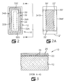
- Figs. 2-6 provide illustrations of the preferred methods, according to the invention, for relieving thermal stresses in the components during a manufacturing process therefor.
- Fig. 2 is a top plan view, not to scale, of a printhead structure 10 prior to attaching a nozzle plate 26 thereto which contains a semiconductor substrate 12 and a polymeric film or polymeric layer 22 attached to a surface of the substrate 12 and which illustrates the improvements according to the invention.
- the polymeric layer 22 is selectively thick, in that it preferably has a thickness ranging from about 2 to about 50 microns, preferably from about 10 to about 30 microns.
- the polymeric layer or film 22 contains a substantially central region 30 in which flow features for ink as described with reference to Fig. 1 are contained and an outer region 32 surrounding the central region containing sufficient valleys, voids or other discontinuities which serve as expansion areas for reducing thermal stresses produced during the manufacturing process.
- the outer region 32 completely surrounds the central region 30 of the polymeric layer 22.
- at least side regions 32A and 32B adjacent the central region 30 contain valleys for reducing thermal stresses while end regions 32C and 32D need not contain such valleys.
- Side regions 32A and 32B are between the ink chambers 20A and 20B (Fig. 1) and the edges 34A and 34B of layer 22.
- Fig. 2A illustrates an alternative embodiment of the invention wherein the ink flows to the flow features of the polymeric layer 22' from the around the edges of the semiconductor substrate 12'.
- the flow features are patterned in the polymeric layer 22' generally in outer region 30' which extends from the edges 34A' and 34B' of the polymeric layer 22' to a central region 32' which contains the valleys for reducing thermal stresses during the process of bonding a nozzle plate to the polymeric layer 22'.
- FIG. 3 A partial cross-sectional view of a side portion of a printhead composite structure 10 according to the invention along view A-A of Fig. 2 is illustrated in Fig. 3.
- the printhead composite structure 10 preferably includes a semiconductor substrate 12, a polymeric layer 22 attached to the substrate 12 and a nozzle plate 26 attached to the polymeric layer 22.
- the polymeric layer 22 preferably contains a plurality of valleys or voids 36 which inhibit thermal stresses in the structure 10 when the nozzle plate 26 is fixedly attached to the polymeric layer 22 of the structure.
- the valleys or voids 36 may be provided with a variety of shapes such as straight, curved or sloped walls, and may have a depth at least as thick as the polymeric layer 22 as shown in Fig. 5 (36A) or a depth that is at least 33% of the thickness of the polymeric layer 22 as shown in Fig. 4.
- the valleys 36 are preferably formed so that they lie substantially perpendicular to the longest dimension of side regions 32A and 32B and substantially perpendicular to the longest dimension of end regions 32C and 32D (Fig. 2).
- the valleys 36 may be patterned in the polymeric layer 22 either before or alter applying the polymeric layer to the substrate 12. The same patterning techniques using a mask may be used to form the valleys 36 as is used to define the flow features in layer 22. In the alternative, the valleys may be mechanically abraded in the polymeric layer 22 using a grinding wheel or other abrasive device. Because the valleys are contained in the polymeric layer 22, there is no need to provide gaps or surface roughness on the metal or metal coated nozzle plate. Accordingly, the manufacturing steps for the printhead structure are greatly simplified particularly since the valleys can be formed at the same time or substantially the same time as the other flow features in the polymeric layer 22.
- the valleys 36 need not extend completely through the polymeric layer 22 to be effective. Accordingly, the depth of the valleys 36 may be controlled by selecting various aspect ratios for the valleys.
- the aspect ratio of a valley is defined as the greatest width of the valley divided by the thickness of the polymeric material used for the polymeric layer. For example, for a photoresist acrylate material such as LEARONAL having a thickness of about 30 microns, an aspect ratio of greater than about 18/30 will provide a valley having a depth equal to the thickness of the polymeric material. Accordingly, masks having widths of greater than 18 up to about 30 microns will produce valleys which extend completely through the polymeric material.
- the polymeric layer 50 has a thickness T of 30 microns.
- the depth D of the valley 52 is equal to the thickness T of the polymeric layer 50.
- valley 54 having a width W' of less than 18 microns, the depth D' of the valley 54 is less than the thickness T of the polymeric layer.
- the aspect ratio for the foregoing material requires an aspect ratio of less than about 18/30 in order to create a valley which does not extend all the way through the polymeric layer
- the particular light source, hardware capabilities, polymeric materials and other factors may affect the aspect ratio for a particular polymeric material. Accordingly, one skilled in the art may readily determine the aspect ratio for any particular polymeric material in order to produce valleys of the desired depth.
Landscapes
- Engineering & Computer Science (AREA)
- Manufacturing & Machinery (AREA)
- Physics & Mathematics (AREA)
- Optics & Photonics (AREA)
- Particle Formation And Scattering Control In Inkjet Printers (AREA)
Applications Claiming Priority (2)
| Application Number | Priority Date | Filing Date | Title |
|---|---|---|---|
| US990343 | 1997-12-15 | ||
| US08/990,343 US6106096A (en) | 1997-12-15 | 1997-12-15 | Printhead stress relief |
Publications (3)
| Publication Number | Publication Date |
|---|---|
| EP0925932A2 true EP0925932A2 (de) | 1999-06-30 |
| EP0925932A3 EP0925932A3 (de) | 2000-02-02 |
| EP0925932B1 EP0925932B1 (de) | 2004-09-22 |
Family
ID=25536058
Family Applications (1)
| Application Number | Title | Priority Date | Filing Date |
|---|---|---|---|
| EP98310285A Expired - Lifetime EP0925932B1 (de) | 1997-12-15 | 1998-12-15 | Druckkopfspannungsentlastung |
Country Status (7)
| Country | Link |
|---|---|
| US (1) | US6106096A (de) |
| EP (1) | EP0925932B1 (de) |
| JP (1) | JPH11263015A (de) |
| KR (1) | KR19990063070A (de) |
| CN (1) | CN1101755C (de) |
| DE (1) | DE69826428T2 (de) |
| TW (1) | TW418160B (de) |
Cited By (6)
| Publication number | Priority date | Publication date | Assignee | Title |
|---|---|---|---|---|
| WO2001054863A3 (en) * | 2000-01-26 | 2002-04-04 | Hewlett Packard Co | Ink feed slot formation in ink-jet printheads |
| EP0999056B1 (de) * | 1998-11-04 | 2006-04-12 | Microjet Technology Co., Ltd | Verfahren für die Herstellung eines Tintenstrahldruckkopfes |
| WO2007092241A1 (en) * | 2006-02-08 | 2007-08-16 | Eastman Kodak Company | A printhead and method of forming same |
| US7914127B2 (en) | 2005-05-31 | 2011-03-29 | Telecom Italia S.P.A. | Nozzle plate for an ink jet print head comprising stress relieving elements |
| WO2011054557A1 (en) * | 2009-11-06 | 2011-05-12 | International Business Machines Corporation | Bilayer systems including a polydimethylglutarimide-based bottom layer and compositions thereof |
| DE10124822B4 (de) * | 2000-05-22 | 2011-11-03 | Toyota Jidosha Kabushiki Kaisha | Sensorvorrichtung und Sensorgerät |
Families Citing this family (16)
| Publication number | Priority date | Publication date | Assignee | Title |
|---|---|---|---|---|
| JP2001001520A (ja) * | 1999-06-21 | 2001-01-09 | Canon Inc | 液体噴射記録ヘッド |
| US6294317B1 (en) * | 1999-07-14 | 2001-09-25 | Xerox Corporation | Patterned photoresist structures having features with high aspect ratios and method of forming such structures |
| US6740536B2 (en) * | 2001-10-26 | 2004-05-25 | Hewlett-Packard Develpment Corporation, L.P. | Devices and methods for integrated circuit manufacturing |
| US6527368B1 (en) | 2002-04-30 | 2003-03-04 | Hewlett-Packard Company | Layer with discontinuity over fluid slot |
| US20040021741A1 (en) * | 2002-07-30 | 2004-02-05 | Ottenheimer Thomas H. | Slotted substrate and method of making |
| US6666546B1 (en) * | 2002-07-31 | 2003-12-23 | Hewlett-Packard Development Company, L.P. | Slotted substrate and method of making |
| US20050157103A1 (en) * | 2004-01-21 | 2005-07-21 | Kia Silverbrook | Ink fluid delivery system for a printer |
| US7152951B2 (en) * | 2004-02-10 | 2006-12-26 | Lexmark International, Inc. | High resolution ink jet printhead |
| US7198353B2 (en) * | 2004-06-30 | 2007-04-03 | Lexmark International, Inc. | Integrated black and colored ink printheads |
| JP2007076015A (ja) * | 2005-09-12 | 2007-03-29 | Sony Corp | 液体吐出ヘッド |
| JP5183187B2 (ja) * | 2007-12-14 | 2013-04-17 | キヤノン株式会社 | 液体吐出ヘッド |
| KR101520623B1 (ko) | 2008-10-01 | 2015-05-18 | 삼성전자주식회사 | 잉크젯 프린트헤드 및 그 제조방법 |
| US8870345B2 (en) * | 2012-07-16 | 2014-10-28 | Xerox Corporation | Method of making superoleophobic re-entrant resist structures |
| CN105408117B (zh) * | 2013-06-28 | 2017-08-25 | 惠普发展公司,有限责任合伙企业 | 打印头结构 |
| WO2015116027A1 (en) | 2014-01-28 | 2015-08-06 | Hewlett-Packard Development Company, L.P. | Printbars and methods of forming printbars |
| JP7292998B2 (ja) * | 2019-06-24 | 2023-06-19 | 東芝テック株式会社 | インクジェットヘッド及びインクジェットプリンタ |
Family Cites Families (5)
| Publication number | Priority date | Publication date | Assignee | Title |
|---|---|---|---|---|
| US4994825A (en) * | 1988-06-30 | 1991-02-19 | Canon Kabushiki Kaisha | Ink jet recording head equipped with a discharging opening forming member including a protruding portion and a recessed portion |
| US5194877A (en) * | 1991-05-24 | 1993-03-16 | Hewlett-Packard Company | Process for manufacturing thermal ink jet printheads having metal substrates and printheads manufactured thereby |
| JP3351436B2 (ja) * | 1991-08-21 | 2002-11-25 | セイコーエプソン株式会社 | 細孔を有する2部材の接着用シ−ト材 |
| US5493320A (en) * | 1994-09-26 | 1996-02-20 | Lexmark International, Inc. | Ink jet printing nozzle array bonded to a polymer ink barrier layer |
| US5847725A (en) * | 1997-07-28 | 1998-12-08 | Hewlett-Packard Company | Expansion relief for orifice plate of thermal ink jet print head |
-
1997
- 1997-12-15 US US08/990,343 patent/US6106096A/en not_active Expired - Lifetime
-
1998
- 1998-12-15 JP JP10356493A patent/JPH11263015A/ja not_active Withdrawn
- 1998-12-15 KR KR1019980055107A patent/KR19990063070A/ko not_active Withdrawn
- 1998-12-15 CN CN98127124A patent/CN1101755C/zh not_active Expired - Fee Related
- 1998-12-15 DE DE69826428T patent/DE69826428T2/de not_active Expired - Lifetime
- 1998-12-15 EP EP98310285A patent/EP0925932B1/de not_active Expired - Lifetime
-
1999
- 1999-03-06 TW TW087120820A patent/TW418160B/zh not_active IP Right Cessation
Cited By (11)
| Publication number | Priority date | Publication date | Assignee | Title |
|---|---|---|---|---|
| EP0999056B1 (de) * | 1998-11-04 | 2006-04-12 | Microjet Technology Co., Ltd | Verfahren für die Herstellung eines Tintenstrahldruckkopfes |
| WO2001054863A3 (en) * | 2000-01-26 | 2002-04-04 | Hewlett Packard Co | Ink feed slot formation in ink-jet printheads |
| DE10124822B4 (de) * | 2000-05-22 | 2011-11-03 | Toyota Jidosha Kabushiki Kaisha | Sensorvorrichtung und Sensorgerät |
| US7914127B2 (en) | 2005-05-31 | 2011-03-29 | Telecom Italia S.P.A. | Nozzle plate for an ink jet print head comprising stress relieving elements |
| WO2007092241A1 (en) * | 2006-02-08 | 2007-08-16 | Eastman Kodak Company | A printhead and method of forming same |
| WO2011054557A1 (en) * | 2009-11-06 | 2011-05-12 | International Business Machines Corporation | Bilayer systems including a polydimethylglutarimide-based bottom layer and compositions thereof |
| GB2487130A (en) * | 2009-11-06 | 2012-07-11 | Ibm | Bilayer systems including a polydimethylglutarimide-based bottom layer and compositions thereof |
| CN102597048A (zh) * | 2009-11-06 | 2012-07-18 | 国际商业机器公司 | 包括基于聚二甲基戊二酰亚胺的底层的双层体系及其组成 |
| US8323868B2 (en) | 2009-11-06 | 2012-12-04 | International Business Machines Corporation | Bilayer systems including a polydimethylglutarimide-based bottom layer and compositions thereof |
| GB2487130B (en) * | 2009-11-06 | 2014-01-08 | Ibm | Bilayer systems including a polydimethylglutarimide-based bottom layer and compositions thereof |
| CN102597048B (zh) * | 2009-11-06 | 2014-03-26 | 国际商业机器公司 | 包括基于聚二甲基戊二酰亚胺的底层的双层体系及其组成 |
Also Published As
| Publication number | Publication date |
|---|---|
| KR19990063070A (ko) | 1999-07-26 |
| TW418160B (en) | 2001-01-11 |
| EP0925932B1 (de) | 2004-09-22 |
| JPH11263015A (ja) | 1999-09-28 |
| CN1229727A (zh) | 1999-09-29 |
| DE69826428T2 (de) | 2006-02-23 |
| EP0925932A3 (de) | 2000-02-02 |
| US6106096A (en) | 2000-08-22 |
| CN1101755C (zh) | 2003-02-19 |
| DE69826428D1 (de) | 2004-10-28 |
Similar Documents
| Publication | Publication Date | Title |
|---|---|---|
| EP0925932B1 (de) | Druckkopfspannungsentlastung | |
| DE3507338C2 (de) | ||
| EP0646466A2 (de) | Druckpatronengehäuse und Düsenkörper | |
| US20090065473A1 (en) | Manufacturing method for liquid discharge head substrate | |
| US6310641B1 (en) | Integrated nozzle plate for an inkjet print head formed using a photolithographic method | |
| KR100445004B1 (ko) | 모노리틱 잉크 젯 프린트 헤드 및 이의 제조 방법 | |
| KR100271138B1 (ko) | 잉크젯 프린트 헤드 및 그 제조 방법 | |
| EP1559554B1 (de) | Verfahren zur Herstellung eines Tintenstrahldruckkopfes | |
| US4570167A (en) | Ink jet recording head | |
| US5450108A (en) | Ink jet printhead which avoids effects of unwanted formations developed during fabrication | |
| US6368515B1 (en) | Method of manufacturing ink-jet printer head | |
| KR100225082B1 (ko) | 프린트 헤드의 잉크 분사 장치 구조 | |
| JP7134831B2 (ja) | 液体吐出ヘッドの製造方法 | |
| JP7195792B2 (ja) | 基板の加工方法、並びに、液体吐出ヘッド用基板およびその製造方法 | |
| KR20030083616A (ko) | 액체 사출 장치, 프린터 헤드, 및 액체 사출 장치 제조 방법 | |
| US6684504B2 (en) | Method of manufacturing an imageable support matrix for printhead nozzle plates | |
| JPH08142327A (ja) | インクジェット記録装置の記録ヘッド | |
| EP2026973B1 (de) | Tintenstrahldruckkopfplatte und herstellungsverfahren dafür | |
| JP3175335B2 (ja) | インクジェットヘッドの製造方法 | |
| JPS59194857A (ja) | インクジエツト記録ヘツド製造方法 | |
| JP2006167969A (ja) | インクジェット記録ヘッドの製造方法 | |
| JPH0578150A (ja) | インクジエツトヘツドの製造方法 |
Legal Events
| Date | Code | Title | Description |
|---|---|---|---|
| PUAI | Public reference made under article 153(3) epc to a published international application that has entered the european phase |
Free format text: ORIGINAL CODE: 0009012 |
|
| AK | Designated contracting states |
Kind code of ref document: A2 Designated state(s): DE FR GB |
|
| AX | Request for extension of the european patent |
Free format text: AL;LT;LV;MK;RO;SI |
|
| RIN1 | Information on inventor provided before grant (corrected) |
Inventor name: WILLIAMS, GARY RAYMOND Inventor name: RAULINAITIS, MICHAEL Inventor name: MURTHY, ASHOK Inventor name: KOMPLIN, STEVEN ROBERT |
|
| PUAL | Search report despatched |
Free format text: ORIGINAL CODE: 0009013 |
|
| AK | Designated contracting states |
Kind code of ref document: A3 Designated state(s): AT BE CH CY DE DK ES FI FR GB GR IE IT LI LU MC NL PT SE |
|
| AX | Request for extension of the european patent |
Free format text: AL;LT;LV;MK;RO;SI |
|
| 17P | Request for examination filed |
Effective date: 20000712 |
|
| AKX | Designation fees paid |
Free format text: DE FR GB |
|
| GRAP | Despatch of communication of intention to grant a patent |
Free format text: ORIGINAL CODE: EPIDOSNIGR1 |
|
| GRAS | Grant fee paid |
Free format text: ORIGINAL CODE: EPIDOSNIGR3 |
|
| GRAA | (expected) grant |
Free format text: ORIGINAL CODE: 0009210 |
|
| AK | Designated contracting states |
Kind code of ref document: B1 Designated state(s): DE FR GB |
|
| REG | Reference to a national code |
Ref country code: GB Ref legal event code: FG4D |
|
| REF | Corresponds to: |
Ref document number: 69826428 Country of ref document: DE Date of ref document: 20041028 Kind code of ref document: P |
|
| PLBE | No opposition filed within time limit |
Free format text: ORIGINAL CODE: 0009261 |
|
| STAA | Information on the status of an ep patent application or granted ep patent |
Free format text: STATUS: NO OPPOSITION FILED WITHIN TIME LIMIT |
|
| ET | Fr: translation filed | ||
| 26N | No opposition filed |
Effective date: 20050623 |
|
| PGFP | Annual fee paid to national office [announced via postgrant information from national office to epo] |
Ref country code: GB Payment date: 20101229 Year of fee payment: 13 |
|
| PGFP | Annual fee paid to national office [announced via postgrant information from national office to epo] |
Ref country code: FR Payment date: 20120104 Year of fee payment: 14 |
|
| PGFP | Annual fee paid to national office [announced via postgrant information from national office to epo] |
Ref country code: DE Payment date: 20111229 Year of fee payment: 14 |
|
| GBPC | Gb: european patent ceased through non-payment of renewal fee |
Effective date: 20121215 |
|
| REG | Reference to a national code |
Ref country code: FR Ref legal event code: ST Effective date: 20130830 |
|
| REG | Reference to a national code |
Ref country code: DE Ref legal event code: R119 Ref document number: 69826428 Country of ref document: DE Effective date: 20130702 |
|
| PG25 | Lapsed in a contracting state [announced via postgrant information from national office to epo] |
Ref country code: DE Free format text: LAPSE BECAUSE OF NON-PAYMENT OF DUE FEES Effective date: 20130702 |
|
| PG25 | Lapsed in a contracting state [announced via postgrant information from national office to epo] |
Ref country code: GB Free format text: LAPSE BECAUSE OF NON-PAYMENT OF DUE FEES Effective date: 20121215 Ref country code: FR Free format text: LAPSE BECAUSE OF NON-PAYMENT OF DUE FEES Effective date: 20130102 |