EP0926570A2 - Gerät und Verfahren zur Potential-messung - Google Patents
Gerät und Verfahren zur Potential-messung Download PDFInfo
- Publication number
- EP0926570A2 EP0926570A2 EP98124655A EP98124655A EP0926570A2 EP 0926570 A2 EP0926570 A2 EP 0926570A2 EP 98124655 A EP98124655 A EP 98124655A EP 98124655 A EP98124655 A EP 98124655A EP 0926570 A2 EP0926570 A2 EP 0926570A2
- Authority
- EP
- European Patent Office
- Prior art keywords
- potential
- sensor
- detecting portion
- measured
- potential sensor
- Prior art date
- Legal status (The legal status is an assumption and is not a legal conclusion. Google has not performed a legal analysis and makes no representation as to the accuracy of the status listed.)
- Granted
Links
Images

















Classifications
-
- G—PHYSICS
- G03—PHOTOGRAPHY; CINEMATOGRAPHY; ANALOGOUS TECHNIQUES USING WAVES OTHER THAN OPTICAL WAVES; ELECTROGRAPHY; HOLOGRAPHY
- G03G—ELECTROGRAPHY; ELECTROPHOTOGRAPHY; MAGNETOGRAPHY
- G03G15/00—Apparatus for electrographic processes using a charge pattern
- G03G15/50—Machine control of apparatus for electrographic processes using a charge pattern, e.g. regulating differents parts of the machine, multimode copiers, microprocessor control
- G03G15/5033—Machine control of apparatus for electrographic processes using a charge pattern, e.g. regulating differents parts of the machine, multimode copiers, microprocessor control by measuring the photoconductor characteristics, e.g. temperature, or the characteristics of an image on the photoconductor
- G03G15/5037—Machine control of apparatus for electrographic processes using a charge pattern, e.g. regulating differents parts of the machine, multimode copiers, microprocessor control by measuring the photoconductor characteristics, e.g. temperature, or the characteristics of an image on the photoconductor the characteristics being an electrical parameter, e.g. voltage
-
- G—PHYSICS
- G01—MEASURING; TESTING
- G01R—MEASURING ELECTRIC VARIABLES; MEASURING MAGNETIC VARIABLES
- G01R29/00—Arrangements for measuring or indicating electric quantities not covered by groups G01R19/00 - G01R27/00
- G01R29/12—Measuring electrostatic fields or voltage-potential
Definitions
- the present invention relates to a method for measuring surface potential of a photosensitive body of an electrophotographic image forming apparatus and a method for effecting control on the basis of a measured result.
- Image quality of the output image from the electrophotographic system greatly depends upon sharpness or clearness in various electrophotographic processes, i.e., clearness of writing information, clearness of an electrostatic latent image formed on a surface of a photosensitive body, clearness of a color fine particle (referred to as "toner” hereinafter) image formed on the surface of the photosensitive body, clearness of the toner image after transferred to a transfer sheet and clearness of the image after the toner is fixed.
- toner color fine particle
- Fig. 72 is a schematic view of a known electrophotographic apparatus.
- methods for controlling a charging process or an exposure process on the basis of a result obtained by measuring potential of a surface of a photosensitive body within a macroscopic range are used.
- the photosensitive drum 603 includes a conductive substrate 604, and a surface on which potential is varied.
- a surface 605 of the photosensitive drum 603 is charged by a charger 606, and an electrostatic latent image is formed on the drum by illuminating light from an image signal applying means 607 onto the drum. Distribution of the potential on the surface 605 of the photosensitive drum 603 is measured by the potential sensor 601.
- the electrostatic latent image is developed by a developing device 608 to form a toner image which is in turn transferred, by a transfer charger 610a, onto a transfer sheet conveyed from a transfer sheet supplying system 609 through a pair of resist rollers 614.
- the transfer sheet is separated from the drum by a separation charger 610b, and the separated transfer sheet is sent, through a transfer sheet conveying system 611, to a fixing device 615, where the toner image is fixed to the transfer sheet.
- the transfer sheet is discharged out of the electrophotographic apparatus.
- residual toner remaining on the surface 605 of the photosensitive drum 603 is scraped by a cleaning blade 616 of a cleaning unit 612.
- the remaining electrostatic latent image is erased by an electricity removing light source 613. In this way, a cycle of the processes is completed.
- the charging process is controlled to set the potential Vdark of the surface of the photosensitive body in a dark condition to a predetermined value.
- a reference charging condition at this point i.e., a value of current or voltage to be applied is determined.
- the photosensitive body is illuminated with a single light amount or plural light amounts, so that surface potential values of the photosensitive body are measured in the respective conditions.
- the reference light amount at this point is selected so that the surface potential V1 of the photosensitive body in the exposure becomes the predetermined value.
- Such potential measurement and potential control are performed upon rise-up of the electrophotographic apparatus and on demand. With this arrangement, the potential values Vdark and V1 are kept constant to prevent fluctuation of image density, thereby providing a stable image.
- the above method (1) for example, a method in which the latent image is developed by using toner as the visualizing means and the image is evaluated to guess the electrostatic latent image before development has widely been used.
- a mechanism for measuring and analyzing the image after the development is required.
- this method is not proper from the view point of increase in cost of the apparatus and poor reproductivity, since dispersion in evaluation becomes great when the image is evaluated by the operator of the electrophotographic apparatus.
- this method is not preferable from the view point of environment, since a transfer material (copy sheet) and toner are required for evaluation.
- Japanese Patent Application (Laid Open) No. 5-508708 discloses a method for measuring evenness of the surface potential by using a detecting electrode.
- a potential sensor is arranged in the vicinity of a surface to be measured and dielectric current due to change in potential on the surface to be measured is generated on the potential sensor by effecting a relative movement between the sensor and the surface to be measured, and the evenness of the surface potential is measured by analyzing the result.
- the potential sensor has an edge, and it is characterized that the change in potential of the surface to be measured is detected by the edge of the detecting electrode.
- a means for preventing discharge by applying bias or for preventing discharge by using gas (SF 6 ) having high discharge start pressure is used and a potential sensor is arranged closely spaced apart from a surface to be measured by a distance of about 30 ⁇ m and dielectric current due to change in potential on the surface to be measured is generated on the potential sensor by effecting a relative movement between the sensor and the surface to be measured, and change in gradient of potential of a latent image at an edge portion is measured by analyzing the result. It is characterized that the detection is effected by using the potential sensor of several tens of ⁇ m or less and the measurement gap of several tens of ⁇ m or less.
- the main resolving power is generally 600dpi to 1200dpi. It is required that the latent image potential so generated (referred to as “digital latent image potential” hereinafter), particularly, high image quality such as reproductivity of fine dots and/or thin lines is maintained very stably against fluctuation of environment, thereby providing a sharp image stably.
- a method for detecting distribution of potential of the latent image requires to detect the distribution of the potential of the digital latent image within a small range with a high resolving power, with the result that the control arrangement becomes complicated.
- the depth and the sharpness of the latent image may be varied in accordance with the environment or other factors. For example, as well as occurrence of the above-mentioned high humidity image flow, if the exposure amount is too great, since the latent image is expanded, the reproductivity of the fine dots may not be ensured or the image may become dim (image flow).
- the resolving power of the detecting means in order to control the potential of the digital latent image which is changed in the width of several tens of ⁇ m, the resolving power of the detecting means must be improved up to several tens of ⁇ m.
- the resolving power can be improved to some extent by decreasing an area of the detecting portion of the potential sensor. However, as the area of the detecting portion is decreased, output of the detection signal is also reduced, thereby reducing S/N ratio.
- a distance between the sensor and the drum must be approached up to several tens of ⁇ m and a relative speed between the sensor and the drum must be increased.
- discharge may be generated or measured potential distribution may be distorted.
- a discharge preventing means for preventing the discharge by using gas (SF 6 ) having high discharge start voltage is provided, the apparatus itself becomes more complicated, and, if the relative speed between the sensor and the photosensitive drum is increased, leakage of gas will affect a bad influence upon the charging process.
- the measuring method can preferably be effected simply and easily, and the control is effected on the basis of the measured result to obtain the high quality image stably.
- the control is effective to provide a system capable of extending service interval.
- An object of the present invention is to provide a potential measuring apparatus and a potential measuring method, in which the above-mentioned conventional drawbacks can be eliminated.
- Another object of the present invention is to provide a potential measuring apparatus and a potential measuring method, in which distribution of potential of an electrostatic latent image on a surface of a photosensitive body with high accuracy while improving an S/N ratio.
- Still another object of the present invention is to provide an image forming method and an image forming apparatus, in which a high quality image can be obtained stably for a long term by using improved potential measuring method and potential measuring apparatus, respectively.
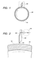
- Fig. 1 is a schematic view showing measurement of configuration of surface potential according to a first embodiment of the present invention.
- the reference numeral 101 denotes a photosensitive drum used in an electrophotographic image forming apparatus such as a copying machine; 102 denotes a surface of the photosensitive drum on which potential is changed; and 103 denotes a potential measuring apparatus acting as a potential measuring means.
- the potential measuring apparatus is constituted by at least one potential sensor (described later), and an insulation support for supporting the potential sensor.
- the other arrangement around the photosensitive drum is the same as that shown in Fig. 72.
- Fig. 2 is a view showing a detailed structure of the potential measuring apparatus 103 shown in Fig. 1.
- the reference numeral 201 denotes a potential sensor
- 202 denotes an insulation support
- 203 denotes a conductive lead
- 204 denotes a circuit element.
- the potential sensor 201 is characterized in that a section of a detecting portion taken along a plane perpendicular to the surface 102 and parallel to a relative movement direction between the potential sensor 201 and the surface 102 has no edge.
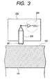
- Fig. 3 is a schematic side view of the potential measuring apparatus 103 shown in Fig. 2. As shown in Figs. 2 and 3, the detecting portion of the potential sensor 201 is connected to the circuit element 204 via the conductive lead 203.
- dielectric current proportional to dV/dt (dV/dx)•(dx/dt) is generated in the potential sensor 201.
- the detected dielectric current includes information relating to gradient of surface potential.
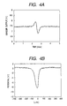
- Figs. 4A and 4B and Figs. 5A and 5B are graphs showing measured results obtained by effecting measurement in a condition that surface potential in a dark condition (in which the photosensitive body is not illuminated) is set to 100V.
- Figs. 4A and 4B are graphs showing measured results of a one-pixel (referred to as "dot", if desired) digital latent image formed by a laser exposure device having scan line density of 600dpi
- Figs. 5A and 5B are graphs showing measured results of a one-dot/one-space digital latent image formed by a laser exposure device having scan line density of 600dpi.
- Figs. 4A and 4B are graphs showing measured results of a one-pixel (referred to as "dot", if desired) digital latent image formed by a laser exposure device having scan line density of 600dpi
- Figs. 5A and 5B are graphs showing measured results of a one-dot/one-space digital latent
- FIGS. 4A and 5A show the potential configurations in a form of a detected waveform
- Figs. 4B and 5B show the potential configurations in a form of a waveform after integration analysis.
- the digital latent image can be measured with very high accuracy.
- the potential sensor 201 can be formed from a conductive wire.
- a diameter of the wire greatly affects an influence upon a detecting resolving power.
- the diameter of the wire is desirable to be smaller as can be possible, if the diameter is decreased, since signal intensity is reduced accordingly, the diameter of the wire has lower limitation. It is desirable that the diameter of the wire is within a range of ⁇ 1 ⁇ m to 500 ⁇ m.
- a length of the signal detecting portion of the potential sensor in a direction transverse to the relative movement direction i.e., in an axial direction of the photosensitive drum
- linearity and parallelism of the wire are apt to be worsened to cause reduction in the resolving power.
- the length of the wire is within a range of 0.2mm to 10mm.
- the detecting portion is arranged to be in parallel with the surface to be measured and in perpendicular to the relative movement direction.
- the detecting resolving power greatly depends upon the linearity and parallelism of the detecting portion of the potential sensor, and, thus, it is preferable that the linearity and parallelism (regarding the direction parallel to the surface to be measured and perpendicular to the relative movement direction (direction perpendicular to the plane of Fig. 2)) of the detecting electrode are within 300%.
- the detected signal i.e., dielectric current is proportional to the relative movement speed as mentioned above. That is to say, by increasing the relative movement speed, the signal intensity is increased, thereby obtaining a good signal. However, if the speed is too high, due to influence of time constant based on the connected circuit element, the S/N ratio may be worsened.
- the relative movement speed is within a range of 10mm/sec to 10000mm/sec. It is not so preferable that a distance between the potential sensor and the surface to be measured (referred to as “measurement interval" herein after) is changed during the relative movement.
- a distance between the potential sensor and the surface to be measured referred to as “measurement interval” herein after
- a mechanism for keeping the distance constant mechanically by using a roller or a spacer or a method in which the distance is monitored by a laser gap sensor or an eddy current displacement sensor and control is effected by a motor to always keep the distance constant.
- a set value of the measurement interval affects an influence upon measurement accuracy.
- the measurement interval is small. However, if the measurement interval is too small, discharge may be generated between the potential sensor and the surface, thereby distorting the electric field. To avoid this, it is preferable that the measurement interval is within a range of 10 ⁇ m to 300 ⁇ m. Incidentally, the interval may be changed before each measurement.
- Material used in the detecting electrode of the potential sensor may be conductive.
- Materials such as W, Au, Pt, Cu, Fe, Ti, Cr, Ag, Ta and the like have excellent conductivity and are suitable for the potential sensor according to the present invention.
- W tungsten
- W has excellent easy-workability and is most suitable for the potential sensor in total.
- one-dimensional (in the relative movement direction) potential configuration can be obtained by a signal from the single potential sensor.
- two-dimensional potential configuration of the surface to be measured can be measured.
- Such plurality of electrodes are disposed side by side along a direction perpendicular to the relative movement direction, i.e., the axial direction of the photosensitive drum (i.e., direction substantially perpendicular to the plane of Figure) in the apparatus shown in Figs. 1 to 3.
- the relative movement between the potential sensor and the surface is generated by rotation of the photosensitive drum.
- the surface is movable with respect to the potential sensor.
- the potential sensor may be movable with respect to the surface.
- the present invention is not limited to such embodiments.
- the detecting resolving power in the tests is evaluated as 1/e 2 half value width of a potential signal obtained when a digital latent image corresponding to one pixel is measured.
- Fig. 6 shows a measured result of the potential configuration of the digital latent image obtained by a laser exposure device having scan line density of 400dpi to 1200dpi in a test effected by using the potential configuration measuring apparatus shown in Fig. 1. Measuring conditions are as shown in the following Table 1: Wire diameter 1 to 100 [ ⁇ m] Wire length 1 [mm] measurement interval 10 [ ⁇ m] relative movement speed 300 [mm/sec]
- the detecting resolving power strongly depends upon the diameter of the wire, and, as the diameter of the wire is decreased, the detecting resolving power is improved. Namely, in the measured result of the digital latent image having 1200dpi, when the diameter of the wire becomes smaller than a diameter ( ⁇ 20 ⁇ m) of a spot of the laser, the potential configuration can be measured with a high resolving power nearer to the diameter of the laser spot. Similarly, also in case of 600dpi and 400dpi, when the wire diameter is smaller than the diameter of the laser spot, the resolving power near the spot diameter can be obtained. Incidentally, even when the potential sensor having the wire diameter of 1 ⁇ m is used, a good signal having excellent S/N ratio can be obtained.
- Fig. 7 shows a detailed result of a relation between the diameter of the wire and the signal intensity.
- the change in potential in this case is formed by image exposure having a width of 2mm so that it becomes greater than the diameter of the wire.
- the signal intensity is decreased. That is to say, it was found that, in a range where the wire diameter exceeds 500 ⁇ m, both the detecting resolving power and the signal intensity are worsened, which is not suitable for the measurement of the surface potential configuration according to the present invention.
- Figs. 8 and 9 show test results providing a relation between a length of the wire used in the potential sensor and the detecting resolving power and a relation between the wire length and the signal intensity in tests effected by using the potential configuration measuring apparatus shown in Fig. 1. Measuring conditions are as shown in the following Table 2: Wire diameter 10 [ ⁇ m] Wire length 0.1 to 15 [mm] measurement interval 10 [ ⁇ m] relative movement speed 300 [mm/sec] scan line density 600 [dpi]
- the length of the wire is associated with the signal intensity and the detecting resolving power.
- the detecting resolving power is worsened.
- an absolute value of the detecting resolving power strongly depends upon the wire diameter more than the wire length.
- the detecting resolving power is worsened about twice in comparison with the case where the length of the wire is 1mm.
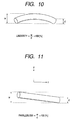
- Fig. 10 is an enlarged view of a detecting portion of a potential sensor specially manufactured for these tests, looked at from a direction shown in Fig. 3.
- the potential sensor is manufactured so that the detecting portion has intentionally a curved shape, and it is defined so that the linearity is illustrated in the Figure.
- Fig. 11 is a schematic view showing definition of the parallelism.
- a relative movement direction X is perpendicular to the plane of Fig.
- the linearity and parallelism of the wire are associated with the resolving power, and, it was found that, when the linearity and the parallelism are worsened, the detecting resolving power is also worsened.
- an absolute value of the detecting resolving power strongly depends upon the wire diameter more than the linearity and parallelism of the wire.
- Fig. 13 shows a test result providing a relation between the relative movement speed and the signal intensity and distortion of a measured waveform in the test effected by using the potential configuration measuring apparatus shown in Fig. 1. Measuring conditions are as shown in the following Table 4: Wire diameter 10 [ ⁇ m] Wire length 1 [mm] measurement interval 10 [ ⁇ m] relative movement speed 10 to 100000 [mm/sec] scan line density 600 [dpi]
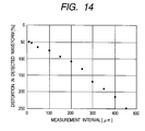
- Fig. 14 shows a test result providing a relation between the measurement interval and the detecting resolving power in the test effected by using the potential configuration measuring apparatus shown in Fig. 1. Measuring conditions are as shown in the following Table 5: Wire diameter 10 [ ⁇ m] Wire length 1 [mm] measurement interval 5 to 500 [ ⁇ m] relative movement speed 300 [mm/sec] scan line density 600 [dpi]
- the measurement interval is 200 ⁇ m or less, and more preferably, 100 ⁇ m or less.
- the measurement interval can be selected voluntarily. If the measurement interval is smaller than 10 ⁇ m, discharge is generated between the surface potential and the potential sensor to distort the detected waveform considerably, thereby making the measurement of the potential configuration of the surface impossible.
- the surface potential measuring apparatus can have a resolving power sufficient to measure the digital latent image in the flat board-shaped photosensitive body and the belt-shaped photosensitive body, as well as the drum-shaped photosensitive body.
- the surface potential measuring method according to the illustrated embodiment can be applied to the arrangement in which the potential sensor is movable with respect to the drum surface, as well as the arrangement in which the relative movement between the potential sensor and the drum surface is achieved by the rotation of the photosensitive drum, i.e., the drum surface is movable with respect to the potential sensor.
- the potential sensor in the surface potential measurement wherein the dielectric current generated by the relative movement between the potential sensor and the surface to be measured is detected and analyzed, by using the potential sensor having the characteristic that the sectional shape of the detecting portion of the potential sensor taken along the plane perpendicular to the surface to be measured and parallel to the relative movement direction between the potential sensor and the surface has no edge, there can be provided the more efficient resolving power by about two or three times in comparison with the conventional potential sensor using the flat conductive board as the detecting electrode. Further, even when the width of the detecting electrode, the potential sensor can maintain the signal intensity, thereby providing a signal having excellent S/N ratio. Thus, the digital latent image which was conventionally considered to be hard to measure can be measured and the surface potential configuration thereof can be evaluated.
- Fig. 17 is a view showing a potential measuring apparatus according to a second embodiment of the present invention in detail.
- the reference numeral 301 denotes a potential sensor
- 302 denotes a support
- 303 denotes a conductive lead
- 304 denotes a circuit element
- 305 denotes a shield
- 306 denotes an insulation body.
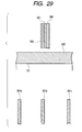
- a detecting portion of the potential sensor 301 is constituted by a board-shaped conductive body having extension extending in a plane perpendicular to a surface to be measured and perpendicular to a relative movement direction, and a conductive portion other than a surface opposed to the surface to be measured is covered by the shield.
- Fig. 18 is a schematic side view of the potential measuring apparatus of Fig. 17. As shown in Figs. 17 and 18, the detecting portion of the potential sensor 301 is connected to the circuit element 304 via the conductive lead 303. Further, in the potential sensor 301, the conductive portion other than the surface opposed to the surface to be measured is covered by the shield 305 via the insulation body 306. If there is no shield 305, when the surface potential was measured, since signals were also detected by the surfaces other than the surface opposed to the surface to be measured, only a signal having bad S/N ratio was obtained, with the result that the potential configuration of the digital latent image could not be measured correctly.
- the detected dielectric current includes information relating to gradient of surface potential.
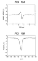
- Figs. 19A and 19B and Figs. 20A and 20B are graphs showing measured results obtained by effecting measurement in a condition that surface potential in a dark condition is set to 100V.
- Figs. 19A and 19B are graphs showing measured results of a one-pixel (referred to as "dot", if desired) digital latent image formed by a laser exposure device having scan line density of 600dpi
- Figs. 20A and 20B are graphs showing measured results of a one-dot/one-space digital latent image formed by a laser exposure device having scan line density of 600dpi.
- Figs. 19A and 20A show the potential configurations in a form of a detected waveform
- 19B and 20B show the potential configurations in a form of a waveform after integration analysis.
- the digital latent image can be measured with very high accuracy.
- the potential sensor 301 has a board-shaped structure.
- a thickness of the board i.e., a thickness of the detecting portion greatly affects an influence upon a detecting resolving power.
- the thickness of the board is desirable to be smaller as can as possible, if the thickness is decreased, since signal intensity is reduced accordingly, the thickness of the board has lower limitation. It is desirable that the thickness is within a range of 1 ⁇ m to 500 ⁇ m.
- a length of the signal detecting portion of the potential sensor in a direction transverse to the relative movement direction i.e., in an axial direction of the photosensitive drum) affects an affects an influence upon intensity of the signal to be detected.
- the length of the detecting portion is within a range of 0.2mm to 10mm.
- the detecting resolving power greatly depends upon the linearity and parallelism of the detecting portion of the potential sensor, and, thus, it is preferable that the linearity and parallelism (regarding the direction parallel to the surface to be measured and perpendicular to the relative movement direction (direction perpendicular to the plane of Fig. 17)) of the detecting electrode are within 300%.
- the detected signal i.e., dielectric current is proportional to the relative movement speed as mentioned above. That is to say, by increasing the relative movement speed, the signal intensity is increased, thereby obtaining a signal having good S/N ratio. However, if the speed is too high, due to influence of time constant based on the connected circuit element, the S/N ratio may be worsened.
- the relative movement speed is within a range of 10mm/sec to 10000mm/sec. It is not so preferable that a distance between the potential sensor and the surface to be measured (referred to as “measurement interval” hereinafter) is changed during the relative movement.
- a distance between the potential sensor and the surface to be measured referred to as “measurement interval” hereinafter
- a mechanism for keeping the distance constant mechanically by using a roller or a spacer or a method in which the distance is monitored by a laser gap sensor or an eddy current displacement sensor and control is effected by a motor to always keep the distance constant.
- a set value of the measurement interval affects an influence upon measurement accuracy.
- the measurement interval is small. However, if the measurement interval is too small, discharge may be generated between the potential sensor and the surface, thereby distorting the electric field. To avoid this, it is preferable that the measurement interval is within a range of 10 ⁇ m to 300 ⁇ m.
- one-dimensional (in the relative movement direction) potential configuration can be obtained by a signal from the signal potential sensor.
- two-dimensional potential configuration of the surface to be measured can be measured.
- Such plurality of electrodes are disposed side by side along a direction perpendicular to the relative movement direction, i.e., the axial direction of the photosensitive drum (i.e., direction substantially perpendicular to the plane of Figure) in the apparatus shown in Figs. 17 and 18.
- the relative movement between the potential sensor and the drum surface is generated by rotation of the photosensitive drum.
- the drum surface is movable with respect to the potential sensor.
- the potential sensor may be movable with respect to the drum surface.
- the present invention is not limited to such embodiments.
- the detecting resolving power in the tests is evaluated as 1/e 2 half value width of a potential signal obtained when a digital latent image corresponding to one pixel measured.
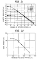
- Fig. 21 shows a measured result of the potential configuration of the digital latent image obtained by a laser exposure device having scan line density of 400dpi to l200dpi in a test effected by using the potential configuration measuring apparatus shown in Fig. 17.
- Measuring conditions are as shown in the following Table 10: thickness of detecting portion 1 to 100 [ ⁇ m] length of detecting portion 1 [mm] measurement interval 10 [ ⁇ m] relative movement speed 300 [mm/sec]
- the detecting resolving power strongly depends upon the thickness of the detecting portion, and, as the thickness is decreased, the detecting resolving power is improved. Namely, in the measured result of the digital latent image having 1200dpi, when the thickness of the detecting portion becomes smaller than a diameter ( ⁇ 20 ⁇ m) of a spot of the laser, the potential configuration can be measured with a high resolving power nearer to the diameter of the laser spot. Similarly, also in case of 600dpi and 400dpi, when the thickness is smaller than the diameter of the laser spot, the resolving power near the spot diameter can be obtained. Incidentally, even when the potential sensor including the detecting portion having a thickness of 1 ⁇ m is used, a signal having excellent S/N ratio can be obtained.
- Fig. 22 shows a detailed result of a relation between the thickness of the detecting portion and the signal intensity.
- the change in potential in this case is formed by image exposure having a width of 2mm so that it becomes greater than the thickness of the detecting portion.
- the signal intensity is decreased. That is to say, it was found that, in a range where the thickness exceeds 500 ⁇ m, both the detecting resolving power and the signal intensity are worsened, which is not suitable for the measurement of the surface potential configuration according to the present invention.
- Figs. 23 and 24 show test results providing a relation between a length of the detecting portion used in the potential sensor and the detecting resolving power and a relation between the wire length and the signal intensity in tests effected by using the potential configuration measuring apparatus shown in Fig. 17. Measuring conditions are as shown in the following Table 11: thickness of detecting portion 10 [ ⁇ m] length of detecting portion 0.1 to 15 [mm] measurement interval 10 [ ⁇ m] relative movement speed 300 [mm/sec]
- the thickness of the detecting portion is associated with the signal intensity and the detecting resolving power. As the thickness of the detecting portion is increased, the detecting resolving power is worsened. However, an absolute value of the detecting resolving power strongly depends upon the thickness of the detecting portion more than the length of the detecting portion. Thus, it is considered that, when the length of the detecting portion is increased, the resolving power inherently included in the wire cannot be reached. According to the result shown in Fig. 23, when the length of the detecting portion is 10mm, the detecting resolving power is worsened about twice in comparison with the case where the length is 1mm. Thus, it is not so preferable to select a length greater than 10mm.
- Fig. 25 is a schematic view showing definition of the parallelism.
- a relative movement direction "X" indicates a relative movement direction
- "Y” indicates a direction perpendicular to the plane of Fig. 25 and perpendicular to the surface to be measured
- "Z” indicates a direction perpendicular to the directions X and Y.
- Test conditions and test result are shown in the following Table 12 and Figs. 16A to 16D, respectively.
- the parallelism of the wire is associated with the resolving power, and, it was found that, when the parallelism is worsened, the detecting resolving power is also worsened.
- an absolute value of the detecting resolving power strongly depends upon the thickness of the detecting portion more than the parallelism.
- the parallelism is worsened, the resolving power inherently included in the wire cannot be reached.
- the parallelism of the wire exceeds 300%, the detecting resolving power is worsened about twice in comparison with the detecting resolving power in the case where the parallelism of the wire is 150%.
- the parallelism of the wire exceeds 300%.
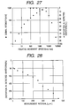
- Fig. 27 shows a test result providing a relation between the relative movement speed and the signal intensity and distortion of a measured waveform in the test effected by using the potential configuration measuring apparatus shown in Fig. 17.
- Measuring conditions are as shown in the following Table 13: thickness of detecting portion 10 [ ⁇ m] length of detecting portion 1 [mm] measurement interval 10 [ ⁇ m] relative movement speed 10 to 100000 [mm/sec] scan line density 600 [dpi]
- Fig. 28 shows a test result providing a relation between the measurement interval and the detecting resolving power in the test effected by using the potential configuration measuring apparatus shown in Fig. 17.
- Measuring conditions are as shown in the following Table 14: thickness of detecting portion 10 [ ⁇ m] length of detecting portion 1 [mm] measurement interval 5 to 500 [ ⁇ m] relative movement speed 300 [mm/sec] scan line density 600 [dpi]
- the measurement interval is 200 ⁇ m or less, and more preferably, 100 ⁇ m or less.
- the measurement interval can be selected voluntarily. If the measurement interval is smaller than 10 ⁇ m, discharge is generate between the surface potential and the potential sensor to distort the detected waveform considerably, thereby making the measurement of the potential configuration of the surface impossible.
- the measurement can be performed with the resolving power near the diameter of the laser spot, thereby obtaining the resolving power sufficient to measure the digital latent image.
- the surface potential measuring apparatus can have a resolving power sufficient to measure the digital latent image in the flat board-shaped photosensitive body and the belt-shaped photosensitive body, as well as the drum-shaped photosensitive body.
- the surface potential measuring method according to the illustrated embodiment can be applied to the arrangement in which the potential sensor is movable with respect to the drum surface, as well as the arrangement in which the relative movement between the potential sensor and the drum surface is achieved by the rotation of the photosensitive drum, i.e., the drum surface is movable with respect to the potential sensor.
- the potential sensor having the characteristic that the sectional shape of the detecting portion of the potential sensor is constituted by the board-shaped conductive body having the extension in the plane perpendicular to the surface to be measured and perpendicular to the relative movement direction and the conductive portion other than the surface opposed to the surface to be measured is covered by the shield so that the dielectric current is not received from the portion other than the surface opposed to the surface to be measured, there can be provided the more efficient resolving power by about two or three times in comparison with the conventional potential sensor using the flat conductive board as the detecting electrode.
- the potential sensor can maintain the signal intensity, thereby providing a signal having excellent S/N ratio.
- the digital latent image which was conventionally considered to be hard to measure can be measured and the surface potential configuration thereof can be evaluated.
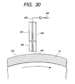
- Fig. 30 is a view showing a potential measuring apparatus according to a third embodiment of the present invention in detail.
- the reference numeral 401 denotes a potential sensor; 402 denotes a support; 403 denotes a conductive lead; and 304 denotes a circuit element.
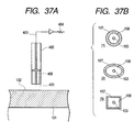
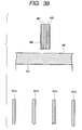
- a detecting portion of the potential sensor 401 is constituted by a rod-shaped conductive body extending in perpendicular to a surface to be measured, and a conductive portion other than a surface opposed to the surface to be measured is covered by the shield so that dielectric current is not received from the portion other than the surface opposed to the surface to be measured.
- the detecting portion of the potential sensor 401 is connected to the circuit element 404 via the conductive lead 403. Further, in the potential sensor 401, the conductive portion other than the surface opposed to the surface to be measured is covered by the shield 305 via an insulation body 406. If there is no shield 405, when the surface potential was measured, since signals were also detected by the surfaces other than the surface opposed to the surface to be measured, only a signal having bad S/N ratio was obtained, with the result that the potential configuration of the digital latent image could not measured correctly.
- the detected dielectric current includes information relating to gradient of surface potential.
- Figs. 31A and 31B and Figs. 32A and 32B are graphs showing measured results obtained by effecting measurement in a condition that surface potential in a dark condition is set to 100V.
- Figs. 31A and 31B are graphs showing measured results of a one-pixel (referred to as "dot", if desired) digital latent image formed by a laser exposure device having scan line density of 600dpi
- Figs. 32A and 32B are graphs showing measured results of a one-dot/one-space digital latent image formed by a laser exposure device having scan line density of 600dpi.
- Figs. 31A and 32A show the potential configurations in a form of a detected waveform
- 31B and 32B show the potential configurations in a form of a waveform after integration analysis.
- the digital latent image can be measured with very high accuracy.
- the potential sensor 301 has a rod-shaped structure.
- a width of a surface of the detecting portion of the potential sensor 401 opposed to the surface to be measured greatly affects an influence upon a detecting resolving power.
- width of detecting portion is desirable to be smaller as can as possible, if the width of the detecting portion is decreased, since signal intensity is reduced accordingly, the width of the detecting portion has lower limitation. It is desirable that the width of the detecting portion is within a range of 1 ⁇ m to 500 ⁇ m.
- the detected signal i.e., dielectric current is proportional to the relative movement speed as mentioned above. That is to say, by increasing the relative movement speed, the signal intensity is increased, thereby obtaining a signal having good S/N ratio. However, if the speed is too high, due to influence of time constant based on the connected circuit element, the S/N ratio may be worsened.
- the relative movement speed is within a range of 10mm/sec to 10000mm/sec. It is not so preferable that a distance between the potential sensor and the surface to be measured (referred to as “measurement interval" herein after) is changed during the relative movement.
- a distance between the potential sensor and the surface to be measured referred to as “measurement interval” herein after
- a mechanism for keeping the distance constant mechanically by using a roller or a spacer or a method in which the distance is monitored by a laser gap sensor or an eddy current displacement sensor and control is effected by a motor to always keep the distance constant.
- a set value of the measurement interval affects an influence upon measurement accuracy.
- the measurement interval is small. However, if the measurement interval is too small, discharge may be generated between the potential sensor and the surface, thereby distorting the electric field. To avoid this, it is preferable that the measurement interval is within a range of 10 ⁇ m to 300 ⁇ m.
- one-dimensional (in the relative movement direction) potential configuration can be obtained by a signal from the single potential sensor.
- two-dimensional potential configuration of the surface to be measured can be measured.
- Such plurality of electrodes are disposed side by side along a direction transverse to the relative movement direction, i.e., the axial direction of the photosensitive drum (i.e., direction substantially perpendicular to the plane of Figure) in the apparatus shown in Fig. 30.
- the relative movement between the potential sensor and the drum surface is generated by rotation of the photosensitive drum.
- the drum surface is movable with respect to the potential sensor.
- the potential sensor may be movable with respect to the drum surface.
- the present invention is not limited to such embodiments.
- the detecting resolving power in the tests is evaluated as 1/e 2 half value width of a potential signal obtained when a digital latent image corresponding to one pixel is measured.
- Fig. 33 shows a measured result of the potential configuration of the digital latent image obtained by a laser exposure device having scan line density of 400dpi to l200dpi in a test effected by using the potential configuration measuring apparatus shown in Fig. 30.
- Measuring conditions are as shown in the following Table 19: width of detecting portion 1 to 500 [ ⁇ m] measurement interval 10 [ ⁇ m] relative movement speed 300 [mm/sec]
- the detecting resolving power strongly depends upon the width of the detecting portion, and, as the width is decreased, the detecting resolving power is improved. Namely, in the measured result of the digital latent image having 1200dpi, when the width of the detecting portion becomes smaller than a diameter ( ⁇ 20 ⁇ m) of a spot of the laser, the potential configuration can be measured with a high resolving power nearer to the diameter of the laser spot. Similarly, also in case of 600dpi and 400dpi, when the width is smaller than the diameter of the laser spot, the resolving power near the spot diameter can be obtained. Incidentally, even when the potential sensor including the detecting portion having a width of 1 ⁇ m is used, a signal having excellent S/N ratio can be obtained.
- Fig. 34 shows a detailed result of a relation between the width of the detecting portion and the signal intensity.
- the change in potential in this case is formed by image exposure having a width of 2mm so that it becomes greater than the width of the detecting portion.
- Fig. 34 it was found that, if the width exceeds 500 ⁇ m, the signal intensity is decreased. That is to say, it was found that, in a range where the width exceeds 500 ⁇ m, both the detecting resolving power and the signal intensity are worsened, which is not suitable for the measurement of the surface potential configuration according to the present invention.
- Fig. 35 shows a test result providing a relation between the relative movement speed and the signal intensity and distortion of a measured waveform in the test effected by using the potential configuration measuring apparatus shown in Fig. 30.
- Measuring conditions are as shown in the following Table 20: width of detecting portion 30 [ ⁇ m] measurement interval 30 [ ⁇ m] relative movement speed 10 to 100000 [mm/sec] scan line density 600 [dpi]
- Fig. 36 shows a test result providing a relation between the measurement interval and the detecting resolving power in the test effected by using the potential configuration measuring apparatus shown in Fig. 30.
- Measuring conditions are as shown in the following Table 21: width of detecting portion 30 [ ⁇ m] measurement interval 5 to 500 [ ⁇ m] relative movement speed 300 [mm/sec] scan line density 600 [dpi]
- the measurement interval is 200 ⁇ m or less, and more preferably, 100 ⁇ m or less.
- the measurement interval can be selected voluntarily. If the measurement interval is smaller than 10 ⁇ m, discharge is generate between the surface potential and the potential sensor to distort the detected waveform considerably, thereby making the measurement of the potential configuration of the surface impossible.
- the surface potential measuring apparatus can have a resolving power sufficient to measure the digital latent image in the flat board-shaped photosensitive body and the belt-shaped photosensitive body, as well as the drum-shaped photosensitive body.
- the surface potential measuring method according to the illustrated embodiment can be applied to the arrangement in which the potential sensor is movable with respect to the drum surface, as well as the arrangement in which the relative movement between the potential sensor and the drum surface is achieved by the rotation of the photosensitive drum, i.e., the drum surface is movable with respect to the potential sensor.
- the potential sensor having the characteristic that the sectional shape of the detecting portion of the potential sensor is constituted by the rod-shaped conductive body extending in perpendicular to the surface to be measured and the conductive portion other than the surface opposed to the surface to be measured is covered by the shield so that the dielectric current is not received from the portion other than the surface opposed to the surface to be measured, there can be provided the more efficient resolving power by about two or three times in comparison with the conventional potential sensor using the flat conductive board as the detecting electrode.
- the potential sensor can maintain the signal intensity, thereby providing a signal having excellent S/N ratio.
- the digital latent image which was conventionally considered to be hard to measure can be measured and the surface potential configuration thereof can be evaluated.
- Fig. 39 is an enlarged view of a potential sensor 4101 used in a first method of a fourth embodiment of the present invention.
- the potential sensor 4101 is characterized in that a detecting portion of the potential sensor 4101 perpendicular to the surface 102 of the photosensitive body 100 and parallel to the relative movement direction between the potential sensor 4101 and the surface 102 is constituted by a rod-shaped conductive body.
- Fig. 40 schematically shows the sensor looked at from the left or right of Fig. 39.
- a relative movement is generated between the potential sensor 4101 and the surface 102
- the relative movement speed can be a surface speed of the photosensitive body 100 (referred to as "process speed" hereinafter).
- the dielectric current detected in this method includes information relating to gradient of surface potential. By integrating and analyzing this data, the surface potential distribution can be measured. Integration constant used in analysis is determined to reproduce the potential distribution when the surface of a photosensitive body having known potential distribution is measured. However, in the analyzing method according to the illustrated embodiment, a width of the detecting portion of the potential sensor 4101 must be smaller than a width of change in potential to be measured.
- the potential sensor 4101 can be constituted by the rod-shaped conductive body.
- the potential sensor 4101 may be formed from conductive material such as gold, copper, iron, aluminium or the like, but, tungsten is best from the view point of easy-workability and cheapness.
- a signal having an S/N ratio more excellent than a flat board shape can be obtained.
- a maximum diameter of the conductive body used referred to as "conductor diameter” hereinafter
- the conductor diameter is as small as possible.
- the conductor diameter has lower limitation. It is desirable that the conductor diameter is within a range of 1 ⁇ m to 100 ⁇ m.
- the potential sensor has the simple structure such as the rod shape, the position of the sensor can mechanically be adjusted relatively easily. That is to say, the maintenance can be facilitated.
- the measurement is hard to be subjected to the influence of arrange distribution along an Z-axis (longitudinal direction) of the photosensitive body, thereby permitting the detection of potential distribution within finer range. Further, this is effective when a latent image forming pattern is formed in the longitudinal direction.
- a length of the signal detecting portion of the potential sensor 4101 in a direction perpendicular to the relative movement direction (i.e., in the longitudinal direction of the photosensitive body 100) affects an influence upon the signal intensity to be detected. If too long, the detecting ability is worsened or manufacture of the detecting portion becomes difficult. To the contrary, if too short, linearity of the rod-shaped conductor (detecting portion) and parallelism with respect to a Y-axis are worsened to result in reduction of the resolving power.
- the length of the rod-shaped conductor is preferably within a range of 0.5mm to 10mm.
- the detecting portion is arranged in parallel to the surface to be measured and in perpendicular to the relative movement direction.
- the detecting resolving power greatly depends upon the linearity and parallelism of the detecting portion of the potential sensor 4101, and, thus, it is preferable that the linearity and parallelism (with respect to the surface to be measured) of the detecting electrode and distortion along the relative movement direction are within a range of 300% or less of the conductor diameter.
- portions of the detecting portion other than a portion adjacent to the photosensitive body 100 may be partially shielded by a shield.
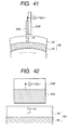
- Fig. 41 is an enlarged view of a potential sensor 5101 used in a second method.
- the potential sensor 5101 used in the second method is characterized in that a detecting portion of the potential sensor 5101 perpendicular to the surface 102 and parallel to the relative movement direction between the potential sensor 5101 and the surface 102 is constituted by a board-shaped conductive body.
- Fig. 42 schematically shows the apparatus looked at from the left or right of Fig. 41.
- a relative movement is generated between the potential sensor 5101 and the surface 102
- the surface potential distribution can be measured.
- a width of the detecting portion of the potential sensor 5101 must be smaller than a width of change in potential to be measured. In this way, the potential sensor 5101 can be formed from the board-shaped conductor.
- the potential sensor 5101 may be formed from conductive material such as gold, copper, iron, aluminium or the like, but, tungsten is best from the view point of easy-workability and cheapness.
- a signal transmitting path from the detecting portion to the analyzing portion provided by other members can be simplified.
- the resistance of such members and joining areas thereof can be reduced, thereby obtaining the signal having excellent S/N ratio.
- a thickness of the conductive body used greatly affects an influence upon the detecting resolving power. Fundamentally, it is desirable that the thickness of the conductive body is as small as possible. However, if too small, since the signal intensity is reduced, the thickness of the conductive body has lower limitation. It is desirable that the thickness of the conductive body is within a range of 1 ⁇ m to 100 ⁇ m.
- the detecting portion of the potential sensor 5101 is arranged in parallel to the surface to be measured and in perpendicular to the relative movement direction.
- the detecting resolving power greatly depends upon the linearity and parallelism of the detecting portion of the potential sensor 5101, and, thus, it is preferable that the linearity and parallelism (with respect to the surface to be measured and to the direction (perpendicular to the plane of Fig. 42) perpendicular to the relative movement direction) of the detecting electrode are within a range of 300% or less of the thickness of the conductive body.
- the potential sensor 5101 having such a detecting portion has the small number of parts and can easily maintain the parallelism and is cheap.
- the thickness and length of the conductive body can be uniformed, thereby obtaining a high accurate detecting portion stably. Further, in the manufacture, the setting of the Z-axis direction can be facilitated, and, thus, a longer sensor or a plurality of sensors can be manufactured. Furthermore, in order to obtain a high S/N ratio, portions of the detecting portion other than a portion adjacent to the surface 102 of the photosensitive body 100 may be electrically shielded by a shield.
- the potential sensor may be movable with respect to the surface of the photosensitive body.
- the present invention is not limited to such embodiments.
- the detecting resolving power in the tests is evaluated as a half value width of a signal obtained when a digital latent image formed by one-line laser exposure is measured by using a laser having a spot diameter of 42 ⁇ m.
- Fig. 43 shows a test result providing a relation between the diameter of the conductive rod used in the potential sensor 4101 and the detecting resolving power in the test effected by the potential distribution measuring apparatus shown in Fig. 39.
- the measuring conditions are shown in the following Table 26. diameter of conductive rod 1 to 200 [ ⁇ m] length of conductive rod 5 [mm] measurement interval 10 [ ⁇ m] relative movement speed 300 [mm/sec]
- the detecting resolving power strongly depends upon the diameter of the conductive rod. Particularly when the conductive rod having a diameter greater then 50 ⁇ m is used, it was difficult to measure the digital latent image separately. Further, when the rod has a diameter up to 1 ⁇ m, a signal having a sufficiently good S/N ratio could be obtained. More preferably, the diameter ( ⁇ ) was 50 ⁇ m.
- Fig. 45 shows a test result providing a relation between the thickness of the conductive board used in the potential sensor 5101 and the detecting resolving power in the test effected by the potential distribution measuring apparatus shown in Fig. 41.
- Measuring conditions are as shown in the following Table 27: Test conditions thickness of conductive board 1 to 200 [ ⁇ m] length of conductive board 1 [mm] measurement interval 10 [ ⁇ m] relative movement speed 300 [mm/sec] * the length of the conductive board is a length of a portion bent at a right angle with respect to a moving direction of an object to be measured
- the detecting resolving power strongly depends upon the thickness of the conductive board. Particularly when the conductive rod having a thickness greater than 50 ⁇ m is used, it was difficult to measure the digital latent image separately. Further, when the rod has a thickness up to 1 ⁇ m, a signal having a sufficiently good S/N ratio could be obtained.
- Figs. 45 and 46 show test results providing a relation between a length of the conductive rod used in the potential sensor 4101 and the detecting resolving power and a relation between the length and the signal intensity in tests effected by using the potential distribution measuring apparatus shown in Fig. 39.
- Measuring conditions are as shown in the following Table 28: Test conditions diameter of conductive rod 1 [ ⁇ m] length of conductive rod 0.1 to 15 [mm] measurement undervalued 10 [ ⁇ m] relative movement speed 300 [mm/sec] scan line density 600 [dpi]
- the length of the conductive rod is associated with the signal intensity and the detecting resolving power.
- the detecting resolving power is worsened.
- an absolute value of the detecting resolving power strongly depends upon the diameter of the conductive rod more than the length of the conductive rod.
- the detecting resolving power inherently included in the wire cannot be reached.
- the detecting resolving power is worsened about twice in comparison with the case where the length of the conductive rod is 1mm.
- the signal intensity is reduced, and, particularly when the length is smaller than 0.5mm, the detection became difficult.
- Figs. 47 and 48 show test results providing a relation between a length of the conductive board used in the potential sensor 5101 and the detecting resolving power and a relation between the length and the signal intensity in tests effected by using the potential distribution measuring apparatus shown in Fig. 41.
- Measuring conditions are as shown in the following Table 29: Test conditions thickness of conductive board 10 [ ⁇ m] length of conductive board 0.1 to 15 [mm] measurement interval 10 [ ⁇ m] relative movement speed 300 [mm/sec] scan line density 600 [dpi] * the length of the conductive board is a length of a portion bent at a right angle with respect to a moving direction of an object to be measured
- the length of the conductive board is associated with the signal intensity and the detecting resolving power.
- the detecting resolving power is worsened.
- an absolute value of the detecting resolving power strongly depends upon the diameter of the conductive board more than the length of the conductive board.
- the detecting resolving power inherently included in the wire cannot be reached.
- the detecting resolving power is worsened about twice in comparison with the case where the length of the conductive board is 1mm.
- the signal intensity is reduced, and, particularly when the length is smaller than 0.5mm, the detection became difficult.
- Fig. 49 shows a test result providing a relation between the relative movement speed and the signal intensity and distortion of a measured waveform in the test effected by using the potential distribution measuring apparatus shown in Fig. 39.
- Measuring conditions are as shown in the following Table 30: Test conditions diameter of conductive rod 50 [ ⁇ m] length of conductive rod 5 [mm] measurement interval 10 [ ⁇ m] relative movement speed 1 to 100000 [mm/sec]
- Fig. 50 shows a test result providing a relation between the relative movement speed and the signal intensity and distortion of a measured waveform in the test effected by using the potential distribution measuring apparatus shown in Fig. 41.
- Measuring conditions are as shown in the following Table 31: Test conditions thickness of conductive board 10 [ ⁇ m] length of conductive board 1 [mm] measurement interval 10 [ ⁇ m] relative movement speed 1 to 100000 [mm/sec]
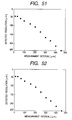
- Fig. 51 shows a test result providing a relation between the measurement interval and the detecting resolving power in the test effected by using the potential distribution measuring apparatus shown in Fig. 39.
- Measuring conditions are as shown in the following Table 32: Test conditions diameter of conductive rod 50 [ ⁇ m] length of conductive rod 5 [mm] measurement interval 5 to 500 [ ⁇ m] relative movement speed 300 [mm/sec] scan line density 600 [dpi]
- Fig. 52 shows a test result providing a relation between the measurement interval and the detecting resolving power in the test effected by using the potential distribution measuring apparatus shown in Fig. 41.
- Measuring conditions are as shown in the following Table 33: Test conditions thickness of conductive board 10 [ ⁇ m] length of conductive board 1 [mm] measurement interval 5 to 500 [ ⁇ m] relative movement speed 300 [mm/sec] scan line density 600 [dpi]
- the measurement interval is 200 ⁇ m or less, and more preferably, 100 ⁇ m or less.
- the measurement interval can be selected voluntarily. If the measurement interval is smaller than 10 ⁇ m, discharge is generate between the surface potential and the potential sensor to distort the detected waveform considerably, thereby making the measurement of the potential configuration of the surface impossible.
- the surface potential measuring apparatus can have a resolving power sufficient to measure the digital latent image in the flat board-shaped photosensitive body and the belt-shaped photosensitive body, as well as the drum-shaped photosensitive body.
- the surface potential measuring method according to the present invention can be applied to the arrangement in which the potential sensors 4101, 5101 are movable with respect to the surface, as well as the arrangement in which the relative movement between the potential sensors 4101, 5101 and the surface is achieved by the rotation of the photosensitive body 100, i.e., the surface is movable with respect to the potential sensor.
- a photosensitive body mainly including a-Si and comprised of a charge-injection preventing layer, a photo-conductive layer and a surface layer was formed on blast-worked aluminium cylinder (support) having a diameter of 180mm under conditions shown in the following Table 40.
- Photosensitive body Kind and flow rate of gas SiH 4 [sccm] 100 200 10 H 2 [sccm] 300 800 B 2 H 6 [sccm] (for SiH 4 ) 2000 2 NO [sccm] CH 4 [sccm] 50 500 Support temp.
- the manufactured photosensitive body was set in an image forming apparatus (obtained by remodeling NP 6060 (manufactured by Canon Inc.) to be suited to the potential sensor of the present invention). Incidentally, the image forming apparatus was remodeled so that the latent image can be written by a laser.
- the potential sensor in the embodiments 1 and 2 was used.
- the shape of the sensor used is shown in the above Table 41.
- the image formation was controlled by using this sensor. Control methods are shown in the following Table 42.
- Vdark control Presence: A sequence in which only Vdark potential is set to a target value is effected by applying voltage/current to a charging portion.
- Vdark control (absence) Vdark potential is determined by applying given voltage/current to a charging member and further control is not effected.
- Vdark potential value is monitored by the potential sensor of the present invention, and Vdc is controlled on the basis of such a value, if necessary.
- V1 control Presence: Change of potential is caused in the charged-up charging member by a laser and the laser output is controlled so that the change of potential becomes a given amount of potential change by integrating and analyzing the dielectric current detected by the potential sensor of the present invention.
- V1 control (absence) Change of potential is caused in the charged-up charging member by a given laser, and the dielectric current (corresponding to the change of potential) detected by the potential sensor of the present invention is integrated and analyzed, and the obtained data is fed back to the Vdark control and Vdc control, if necessary.
- Vdc control Presence: A DC component of developing bias is controlled in dependence upon a value of V1/Vdark.
- Vdc control (absence) The DC component of the developing bias is maintained to a constant value.
- a print endurance test was effected by copying 100,000 (A4 size) sheets by means of this electrophotographic image forming apparatus under an environment shown in the following Table 43.
- the control of image formation was effected as shown in the above Table 42.
- the control shown in the Table 42 was effected automatically every 100 sheets.
- the evaluation of the latent image during the print endurance test was effected on the basis of the image by checking reproductivity of the laser latent image (reproductivity of dots) and change in image density.
- the results of the print endurance test were good in all of the environments, and, during the print endurance test for 100,000 sheets, the quality (dot reproductivity/image density) of the digital images was not worsened.
- the control time can be reduced to about 50% or less in comparison with the well-known potential control (in which Vdark and V1 are independently controlled by know potential sensors), thereby achieving an advantage of reduction of potential control time.
- "1" in V1 is "l" (small L). Environment room temp. [°C] RH [%] number of test sheets A 30 80 100,000 B 20 40 100,000
- a ground layer (intermediate layer) having a thickness of 1 ⁇ m was provided by coating methanol solution including alkoxy-methylated nylon of 5% on an aluminium cylinder (base substrate) having another diameter of 108mm and a length of 358mm by immersion. Then, titanyl-phthalocyanine pigment of 10 weight parts (referred to merely as "parts" hereinafter), polyvinyl butylal of 8 parts and cyclohexanone of 50 parts were mixed and dispersed in a sand mill device using glass beads of 100 parts for 20 hours.
- Methyl-ethyl ketone of 70 to 120 parts was added to the dispersion solution and then was coated on the ground layer, and, by drying this at a temperature of 100°C for 5 minutes, a charge generating layer was formed having a thickness of 0.2 ⁇ m.
- styryl compound of 10 parts and bisphenol Z-type polycarbonate of 10 parts was dissolved in monochlorobenzene of 65 parts. This solution was coated on the charge generating layer by a dipping technique, and, by drying this by hot-air for 60 minutes at a temperature of 120°C, a charge transfer layer having a thickness of 20 ⁇ m was formed. Further, a surface layer having a thickness of about 1 ⁇ m was provided on the transfer layer as a surface protection layer.
- An OPC photosensitive body so manufactured was set in an image forming apparatus (obtained by remodeling NP 6060 (manufactured by Canon Co.) to be suited to the potential sensor of the present invention).
- the image forming apparatus was remodeled so that the latent image can be written by a laser.
- the potential sensor in the embodiments 1 and 2 was used. Control of image formation was effected by using this potential sensor.
- the control methods are the same as those in the embodiment 4 (Table 42). By effecting the same evaluation as that in the embodiment 4, it was ascertained that the same excellent result can be obtained.
- the evaluation of the latent image during the print endurance test was effected on the basis of the image by checking reproductivity of the laser latent image (reproductivity of dots) and change in image density.
- the results of the print endurance test were good in all of the environments, and, during the print endurance test for 10,000 sheets, the quality (dot reproductivity/image density) of the digital images was not worsened.
- the control time can be reduced to about 50% or less in comparison with the well-known potential control (in which Vdark and V1 are independently controlled by know potential sensors), thereby achieving an advantage of reduction of potential control time.
- Fig. 59 shows a result of measurement of a one-pixel latent image formed by laser exposure having scan line density of 600dpi.
- Fig. 60 shows potential configuration of Fig. 59 in the form of a waveform after integration and analysis.
- Fig. 61 shows a result of measurement of a one dot-one space latent image formed by laser exposure having scan line density of 600dpi.
- Fig. 62 shows potential configuration of Fig. 61 in the form of a waveform after integration and analysis.
- the potential configuration of the digital latent image on the photosensitive body 100 particularly, clearness or sharpness and depth of the digital electrostatic latent image are controlled.
- the image forming processes are controlled in accordance with the depth and clearness of the latent image. From the investigation, the Inventors found an electrophotographic image forming apparatus and an electrophotographic image forming method, in which a high quality image can be obtained by controlling one or both of the potential distribution of the digital latent image detected by the above-mentioned potential measuring method and the image forming processes.
- a developing process can be controlled in accordance with the potential distribution in the following manners.
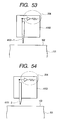
- Fig. 63 schematically shows a developing device (developing means) 1108.
- the developing device 1108 comprises a developing sleeve 1402 including a magnet 1401 therein and adapted to convey toner to the vicinity of the surface of the photosensitive body 100, a doctor blade 1403 as a means for regulating an amount of toner conveyed to the photosensitive body, a voltage applying means (not shown) for applying developing bias to the developing sleeve 1402, and a toner reservoir 1404 for storing the toner.
- the developing bias AC + DC
- Performance of the toner is varied with construction of the toner and is generally divided into two kinds.
- the toner is reciprocated while jumping at a high speed between the developing sleeve 1402 and the photosensitive body 100 by a relation between the developing bias (particularly, an AC component thereof) and a magnetic force of the magnet 1401 of the developing sleeve.
- the toner is developed on the surface 102 of the photosensitive body 100 by a relation between polarity of the toner and the developing bias (particularly, a DC component thereof) and potential of the surface 102 of the photosensitive body 100.
- the toner extends to the surface 102 of the photosensitive body 100 while being connected to the developing sleeve so that to toner is contacted with the surface in the form of a magnet brush.
- the toner is developed on the surface 102 of the photosensitive body 100 by a relation between the developing bias (particularly, the DC component thereof) and the magnetic force of the magnet of the developing sleeve.
- the high quality image can be obtained by controlling the developing means in accordance with the digital electrostatic latent image.
- the developing bias may be controlled in accordance with the depth of the latent image.
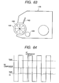
- Fig. 64 schematically shows a relation between the digital electrostatic latent image and the developing bias.
- the DC component of the developing bias is set to a substantially intermediate value between the potential Vdark of the dark portion of the digital electrostatic latent image and the potential VI of the exposure portion.
- the optimum toner image can be obtained by changing the DC component of the developing bias in accordance with the changed potential. If the value VI is increased to decrease the depth of the latent image, the DC component of the developing bias is changed toward an increasing direction. Conversely, if the value Vdark is decreased, the developing bias is decreased. In this way, even if the depth of the latent image is changed, the uniform image can be obtained.
- the control can be effected at real time in use, and, thus, a waiting time of control can be eliminated or be reduced greatly. Further, even if the value Vdark is reduced due to reduction of ability of the charge means or even if the value VI is increased due to reduction of ability of the exposure means, the control can be performed. As a result, interval of the maintenance can be lengthened. Incidentally, the AC component of the developing bias may be controlled.
- the boundary between the Vdark area and the VI area detected by the measuring method according to the illustrated embodiment is obscure, i.e., if the clearness of the latent image is weak, by controlling the SD gap, an area where the toner is developed is changed, thereby obtaining an image having less "fog".
- the development at the boundary can be suppressed by decreasing the SD gap or the development at the boundary can be promoted by increasing the SD gap.
- the SD gap is too great. Further, if too small, the discharge is generated between the toner or the developing means such as the developing sleeve and the photosensitive body 100, thereby affecting a bad influence upon the latent image or preventing the movement of the toner to damage the developing means and/or the photosensitive body 100.
- the SD gap is preferably within a range of 100 ⁇ m to 400 ⁇ m.
- the developing bias value, weight of the toner and charge density it is effective that the SD gap is controlled to a more suitable range.
- a means for controlling the SD gap may be similar to the means for maintaining the distance between the potential sensor and the photosensitive body 100, and other various methods may be used as the control means.
- the digital electrostatic latent image can be controlled.
- the depth and clearness of the latent image on the photosensitive body 100 can be controlled on the basis of the image forming processes, so that the image quality can be improved and a waiting time can be shortened.
- the depth of the digital latent image has a value greater than a predetermined value. Further, in order to obtain a clear image including fine grids and the like, it is preferable that the potential at the boundary between the exposure portion and the non-exposure portion is cleared distinguished from these portions, namely, the clearness of the latent image is excellent. On the other hand, the range of the potential for obtaining the optimum digital electrostatic latent image is varied with the photosensitive body and use condition thereof. By setting the depth and clearness of the latent image to the optimum condition totally, a sharp digital latent image which can reproduce the image signal effectively can be obtained.
- the charge means and/or the image signal applying means are controlled on the basis of the potential distribution of the electrostatic latent image.
- absolute values of Vdark and VI are not necessarily constant.
- the value Vdark has firstly been set by controlling the charge means and then the value VI has been set while controlling the image signal applying means.
- the potential control since a waiting condition is established to limit the use of the apparatus, it is important to reduce the potential control time particularly in case of continuous use such as a printer in a network.
- the values Vdark and VI can be measured simultaneously, the charge means and the image signal applying means can be controlled simultaneously. As a result, the time required for the potential control can be shortened.
- the potential measuring means from the above-mentioned measuring principle, it is preferable that difference in the charge amount in the developing portion is great. However, if too great, adjusting amount of the charging condition such as applied voltage and applied current and the image signal applying condition such as exposure intensity must be increased, with the result that the electrophotographic apparatus becomes complicated and bulky. To avoid this, a photosensitive body 100 in which difference in electricity amount between the values Vdark and VI of the latent image having 40nC/cm 2 to 400nC/cm 2 is used is preferable.
- a preferred photosensitive body 100 may be a photosensitive body including non-crystal silicon as main material, i.e., a photosensitive body of amorphous silicon group (referred to as "a-Si photosensitive body) or a photosensitive body comprised of organic semi-conductor (OPC).
- a-Si photosensitive body a photosensitive body of amorphous silicon group
- OPC organic semi-conductor
- the a-Si photosensitive body Since the a-Si photosensitive body has relatively great electric capacity, the difference in the electricity amount per potential difference becomes great. Thus, such photosensitive body can be used in an area having low Vdark and VI values.
- the difference in electricity amount becomes small.
- the value Vdark is set to be greater to increase the difference in electricity amount so that the photosensitive body may be used to increase the potential difference between the values Vdark and VI.
- the a-Si group photosensitive body may be constituted by a known conductive support and a photo-conductive layer made of non-mono-crystal material based on silicon element, a photosensitive body having improved property can be used, if necessary.
- the a-Si group photosensitive body having the improved property has a photo-conductive layer including hydrogen of 10atom% to 30atom% and is characterized in that property energy of tail (Arback tail) of an exponential function of light absorption spectrum is 50meV to 60meV and local condition density is 1 ⁇ 10 14 cm -3 to 1 ⁇ 10 16 cm -3 .
- the photosensitive body for the image forming apparatus designed to have the above-mentioned construction has very excellent electrical, optical and photo-electrical features, good image quality, good endurance and good use environmental feature, as well as good temperature depending feature of charging ability.
- FIGs. 65 to 70 are schematic structural views for explaining layer structures of photosensitive bodies for the image forming apparatus.
- a photosensitive body 700 for the image forming apparatus shown in Fig. 65 includes a photosensitive layer 702 provided on a support 701 as a photosensitive body.
- the photosensitive layer 702 is constituted by a photo-conductive layer 703 comprising a-Si: H, X and having photo-conductivity.
- Fig. 66 is a schematic constructional view for explaining another layer structure of a photosensitive body for the image forming apparatus.
- the photosensitive body 700 for the image forming apparatus shown in Fig. 66 includes a photosensitive layer 702 provided on a support 701 as a photosensitive body.
- the photosensitive layer 702 is constituted by a photo-conductive layer 703 comprising a-Si: H, X and having photo-conductivity, and a surface layer 704 of amorphous silicon group.
- Fig. 67 is a schematic constructional view for explaining a further layer structure of a photosensitive body for the image forming apparatus.
- the photosensitive body 700 for the image forming apparatus shown in Fig. 67 includes a photosensitive layer 702 provided on a support 701 as a photosensitive body.
- the photosensitive layer 702 is constituted by a photo-conductive layer 703 comprising a-Si: H, X and having photo-conductivity, a surface layer 704 of amorphous silicon group, and a charge injection preventing layer 705 of amorphous silicon group.
- Figs. 68 and 69 are schematic constructional views for explaining a still further layer structure of a photosensitive body for the image forming apparatus.
- the photosensitive body 700 for the image forming apparatus shown in Figs. 68 and 69 includes a photosensitive layer 702 provided on a support 701 as a photosensitive body.
- the photosensitive layer 702 is constituted by a charge transfer layer 708 and a charge generating layer 707 comprising a-Si: H, X and constituting a photo-conductive layer 703, and a surface layer 704 of amorphous silicon group.
- the support 701 may be conductive or insulative.
- the conductive support may be formed from metal such as Al, Cr, Mo, Au, In, Nb, Te, V, Ti, Pt, Pd, Fe or alloy thereof (for example, stainless steel).
- a surface (on which the photosensitive layer is formed) of an electrically insulative support formed from film or sheet of synthetic resin such as polyester, polyethylene, polycarbonate, cellulose acetate, polypropylene, polyvinyl chloride, polystyrene or polyamide, or glass or ceramics may be conductor-treated.
- a shape of the support 701 may be a cylinder or an endless belt having a smooth surface or an uneven surface, and a thickness of the support is appropriately determined so that a desired photosensitive body 700 for the image forming apparatus can be formed.
- the thickness of the support 701 is normally selected to 10 ⁇ m or more in consideration of manufacture, handling and mechanical strength.
- unevenness may be formed on the surface of the support 701 within a range where there is substantially no reduction in light forming carrier.
- the unevenness on the surface of the support 701 may be formed by a well-known method disclosed in Japanese Patent Application Laid-Open Nos. 60-168156, 60-178457, 60-225854 and 61-231561.
- an interference preventing layer or area such as a light absorbing layer may be provided inside or lower side of the photosensitive layer 702.
- fine roughness of the surface of the photosensitive body can be controlled. Formation of the scratches may be effected by using abrasive agent or member or by using etching due to chemical reaction or dry etching or spattering in plasma. In this case, depth and magnitude of the scratches may be included within the range where there is substantially no reduction in light forming carrier.
- the photo-conductive layer 703 can be formed by various thin film deposition methods such as a glow discharge method (AC discharge CVD method such as low frequency CVD method, high frequency CVD method or microwave CVD method, or DC discharge CVD method), a spattering method, a vacuum deposition method, an ion plating method, a light CVD method or a thermal CVD method.
- a glow discharge method AC discharge CVD method such as low frequency CVD method, high frequency CVD method or microwave CVD method, or DC discharge CVD method
- a spattering method such as low frequency CVD method, high frequency CVD method or microwave CVD method, or DC discharge CVD method
- a spattering method such as a spattering method
- a vacuum deposition method such as low frequency CVD method, high frequency CVD method or microwave CVD method, or DC discharge CVD method
- a spattering method such as a spattering method
- a vacuum deposition method such as low frequency CVD method, high frequency CVD method
- These thin film deposition methods are selected and adopted on the basis of various factors such as a manufacturing condition, degree of burden in investment of capital equipments, a manufacturing scale and features required for the photosensitive body for the image forming apparatus.
- the glow discharge method particularly, a high frequency glow discharge method using an RF band, a ⁇ W band or a VHF band is preferable.
- raw material gas capable of supplying silicon atoms (Si) and raw material gas capable of supplying hydrogen atoms (H) or raw material gas capable of supplying halogen atoms (X) may be introduced into a reaction vessel (in which inner pressure can be reduced) in a desired gaseous condition and the glow discharge may be generated in the reaction vessel so that a layer comprised of a-Si: H, X is formed on a predetermined support 701 which was previously installed at a predetermined position.
- a content amount of hydrogen atoms or halogen atoms, or the sum of amounts of the hydrogen atoms and the halogen atoms is 10atom% to 30atom% (preferably, 15atom% to 25atom%) with respect to the sum of the silicon atoms and the hydrogen atoms or/and halogen atoms.
- H 2 gas and/or He gas or gas of silicon compound including hydrogen atoms are required to be mixed with the above-mentioned gases to form the layer. Further, not only each gas alone can be used, but also several kinds of gases can be mixed with a predetermined mixing ratio.
- the raw material gas capable of supplying the halogen atoms used in the illustrated embodiment may be, for example, halogen gas, haride, inter-halogen compound including halogen, or halogen compound such as silane derivative replaced by halogen which is gaseous or can be gasified.
- halogen gas for example, halogen gas, haride, inter-halogen compound including halogen, or halogen compound such as silane derivative replaced by halogen which is gaseous or can be gasified.
- silicon hydride compound including halogen atoms and silicon atoms which is gaseous or can be gasified is also effective.
- the halogen compound which can suitably be used in the illustrated embodiment may concretely be inter-halogen compound such as fluorine gas (F 2 ), BrF, CIF, CIF 3 , BrF 3 , BrF 5 , IF 3 or IF 7 .
- the silicon compound including halogen atoms may concretely be silicon fluoride such as SiF 4 or Si 2 F 6 , for example.
- a temperature of the support 701 an amount of raw material substance (used for including hydrogen atoms or/and halogen atoms) introduced into the reaction vessel, and/or discharge electric power may be controlled.
- atoms for controlling conductivity are included in the photo-conductive layer 703, if necessary.
- the atoms for controlling the conductivity may uniformly be distributed in the photo-conductive layer 703 or be included in the photo-conductive layer partially non-uniformly along a thickness direction.
- the atoms for controlling the conductivity may be so-called impurities in the semi-conductor field, and, as such atoms, atoms belonging to the periodic law table IIIb group giving p-type conductivity (referred to as “IIIb group atoms” hereinafter) or atoms belonging to the periodic law table Vb group giving n-type conductivity (referred to as “Vb group atoms” hereinafter) may be used.
- the IIIb group atom may concretely be boron (B), aluminium (Al), gallium (Ga), indium (In) or thallium (Tl). Particularly, B, Al or Ga is preferable.
- the Vb group atom may concretely be phosphorus (P), arsenic (As), antimony (Sb) or bismuth (Bi) (particularly, P or As is preferable).
- the amount of atoms (for controlling the conductivity) included in the photo-conductive layer 703 is preferably 1 ⁇ 10 -2 atom•ppm - 1 ⁇ 10 4 atom•ppm, and more preferably, 5 ⁇ 10 -2 atom•ppm - 5 ⁇ 10 3 atom•ppm, and most preferably, 1 ⁇ 10 -1 atom•ppm - 1 ⁇ 10 3 atom•ppm.
- raw material substance for introducing the IIIb group atoms or raw material substance for introducing the Vb group atoms may be introduced into the reaction vessel in a gaseous form, together with other gasses for forming the photo-conductive layer 703. It is desirable that gasses which is gaseous under normal temperature and normal pressure or gasses which can easily be gasified at least in the layer forming condition is used as the raw material substance for introducing the IIIb group atoms or raw material substance for introducing the Vb group atoms.
- Such raw material substance for introducing the IIIb group atoms may concretely be boron hydride such as B 2 H 6 , B 4 H 10 , B 5 H 9 , B 5 H 11 , B 6 H 10 , B 6 H 12 or B 6 H 14 or boron haride such as BF 3 , BCl 3 or BBr 3 (for introducing boron atoms).
- boron hydride such as B 2 H 6 , B 4 H 10 , B 5 H 9 , B 5 H 11 , B 6 H 10 , B 6 H 12 or B 6 H 14
- boron haride such as BF 3 , BCl 3 or BBr 3 (for introducing boron atoms).
- AlCl 3 , GaCl 3 , Ga(CH 3 ) 3 , InCl 3 or TlCl 3 may also be used.
- the raw material substance for introducing the Vb group atoms may be phosphorus hydride such as PH 3 or P 2 H 4 or phosphorus haride such as PH 4 I, PF 3 , PF 5 , PCl 3 , PCI 5 , PBr 3 , PBr 5 or PI 3 (for introducing phosphorus atoms).
- AsH 3 , AsF 3 , AsCl 3 , AsBr 3 , AsF 5 , SbH 3 , SbF 3 , SbF 5 , SbCl 3 , SbCI 5 , BiH 3 , BiCl 3 or BiBr 3 may also be used as start substance for introducing the Vb group atoms.
- the raw material substances for introducing the atoms for controlling the conductivity may be diluted by H 2 and/or He, if necessary.
- carbon atoms and/or oxygen atoms and/or nitrogen atoms are included in the photo-conductive layer 703.
- Content amounts of the carbon atoms and/or oxygen atoms and/or nitrogen atoms is preferably 1 ⁇ 10 -5 atom% to 10atom%, and more preferably, 1x10 -4 atom% to 8atom%, and most preferably, 1 ⁇ 10 -3 atom% to 5atom% with respect to the sum of silicon atoms, carbon atoms, oxygen atoms and nitrogen atoms.
- the carbon atoms and/or oxygen atoms and/or nitrogen atoms may uniformly be distributed in the photo-conductive layer or be included in the photo-conductive layer partially non-uniformly along a thickness direction.
- a thickness of the photo-conductive layer 703 is appropriately determined in consideration of the fact that the desired electrophotographic feature can be obtained, the fact that the electric capacity in the use condition is included within the above-mentioned range, and economical effect.
- the thickness is preferably 20 ⁇ m to 50 ⁇ m, and more preferably, 23 ⁇ m to 45 ⁇ m, and most preferably, 25 ⁇ m to 40 ⁇ m.
- the temperature of the support 701 is appropriately selected to the optimum range in accordance with the layer design. Normally, the temperature is preferably 200°C to 350°C, and more preferably, 230°C to 330°C, and most preferably, 250°C to 310°C.
- the conditions for forming the photo-conductive layer are not normally determined independently, but, are desirably determined to optimum values on the basis of organic co-relation to obtain the photosensitive body having the desired features.
- the surface layer 704 of amorphous silicon group is formed on the photo-conductive layer 703 so formed on the support 701.
- the surface layer 704 has a free surface 706 and is provided for achieving the objects of the present invention mainly regarding humidity resistance, continuous use feature, electrical voltage resistance, use environmental feature and endurance.
- the surface layer 704 may be formed from any one of materials of amorphous silicon group.
- amorphous silicon including hydrogen atoms (H) and/or halogen atoms (X) and also including carbon atoms referred to as "a-SiC: H, X” hereinafter
- amorphous silicon including hydrogen atoms (H) and/or halogen atoms (X) and also including oxygen atoms referred to as "a-SiO: H, X” hereinafter
- amorphous silicon including hydrogen atoms (H) and/or halogen atoms (X) and also including nitrogen atoms referred to as "a-SiN: H, X” hereinafter
- amorphous silicon including hydrogen atoms (H) and/or halogen atoms (X) and also including at least one of carbon atoms, oxygen atoms and nitrogen atoms referred to as "a-SiCON: H, X” hereinafter
- the surface layer 704 can be formed, for example, by a well-known thin film deposition method such as a glow discharge method (AC discharge CVD method such as low frequency CVD method, high frequency CVD method or microwave CVD method, or AC discharge method), a spattering method, a vacuum deposition method, an ion plating method, a light CVD method or a thermal CVD method.
- a glow discharge method AC discharge CVD method such as low frequency CVD method, high frequency CVD method or microwave CVD method, or AC discharge method
- a spattering method such as low frequency CVD method, high frequency CVD method or microwave CVD method, or AC discharge method
- a vacuum deposition method such as low frequency CVD method, high frequency CVD method or microwave CVD method, or AC discharge method
- a spattering method such as low frequency CVD method, high frequency CVD method or microwave CVD method, or AC discharge method
- a vacuum deposition method such as low frequency CVD method, high frequency CVD method or microwave CVD method,
- raw material gas capable of supplying silicon atoms (Si), raw material gas capable of supplying carbon atoms (C), and raw material gas capable of supplying hydrogen atoms (H) or/and raw material gas capable of supplying halogen atoms (X) may be introduced into a reaction vessel (in which inner pressure can be reduced) in a desired gaseous condition and the glow discharge may be generated in the reaction vessel so that a surface layer comprised of a-Si: H, X is formed on a predetermined support 701 which was previously installed at a predetermined position and on which the photo-conductive layer 703 was formed.
- the surface layer mainly including a-SiC it is desirable that the content amount of carbon atoms is 30% to 90% with respect to the sum of the silicon atoms and the carbon atoms.
- the content amount of hydrogen atoms included in the surface layer can be greater than 30atom% and smaller than 70atom%, the electric feature and high speed continuous use ability can be improved considerably and high hardness of the surface layer can be ensured.
- the content amount of hydrogen atoms included in the surface layer can be controlled on the basis of a flow rate of H 2 gas, temperature of the support, discharge power and/or gas pressure.
- an amount of raw material substance (used for including hydrogen atoms or/and halogen atoms) introduced into the reaction vessel, and/or discharge electric power may be controlled.
- the carbon atoms and/or oxygen atoms and/or nitrogen atoms may uniformly be distributed in the surface layer or be included in the surface layer partially non-uniformly along a thickness direction.
- atoms for controlling conductivity are included in the surface layer 704, if necessary.
- the atoms for controlling conductivity may uniformly be distributed in the surface layer or be included in the surface layer partially non-uniformly along a thickness direction.
- the atoms for controlling the conductivity may be so-called impurities in the semi-conductor field, and, as such atoms, "IIIb group atoms" or “Vb group atoms” may be used.
- the raw material substance for introducing the atoms for controlling the conductivity may be diluted by gas such as H 2 , He, Ar or Ne, if necessary.
- a thickness of the surface layer 704 is normally 0.01 ⁇ m to 3 ⁇ m, and preferably 0.05 ⁇ m to 2 ⁇ m, and most preferably, 0.1 ⁇ m to 1 ⁇ m. If the surface thickness is smaller than 0.01 ⁇ m, during the usage of the photosensitive body, the surface layer is lost due to wear; whereas, if the thickness is greater than 3 ⁇ m, the electrophotographic feature is worsened due to increase in residual potential.
- a non-crystal carbon film mainly including carbon and having bonding between carbon and fluorine at interior and/or outermost surface thereof (referred to as "a-C: H: F" hereinafter) may be used.
- the a-C: H: F has an excellent water-repelling ability and low friction and further has an effect for preventing obscurity of the image under a high humidity environment in a condition that an environmental countermeasure heater is eliminated, and serves to reduce or prevent damage of the photosensitive body due to mechanical friction of the toner particles.
- the surface layer 704 comprises a-C: H: F
- Hydrocarbon is used as raw material gas and the layer is formed by glow discharge decomposition using high frequency. Since it is desirable that the surface protection layer has high transparency to suppress reduction in sensitivity, gas such as hydrogen, helium or argon is appropriately added, if necessary. Further, a temperature of the substrate is adjusted within a range from a room temperature to 350°C.
- the substance for supplying carbon may be hydrocarbon such as CH 4 , C 2 H 6 , C 3 H 8 or C 4 H 10 which is gaseous or which can be gasified. From the view point of easy handling during the layer formation and good carbon supplying efficiency, CH 4 or C 2 H 6 is preferable.
- the carbon supplying raw material gas may be diluted by gas such as H 2 , He, Ar or Ne, if necessary.
- the electric power should be limited not to generate the abnormal discharge. More specifically, the electric power is preferably 10W/cc or more regarding the hydrocarbon raw material gas and is adjusted appropriately.
- the pressure in the discharge space is selected to 100mmTorr or less, and preferably, 50mTorr or less, and more preferably, 10Torr or less, and a lower limit of the pressure may be selected to a range where the discharge is stabilized.
- gas including fluorine atoms is introduced, and the fluorine atoms are included into the film of the surface protection layer by etching the surface protection layer by generating plasma by means of the appropriate high frequency electric power.
- the electric power is suitably selected within a range from 10W to 5000W in accordance with an etching speed.
- pressure in a treatment space is suitably selected within a range from lmTorr to several Torr.
- the fluorine group gas used for achieving the effect of the present invention may be gas including fluorine such as CF 4 , CHF 3 , C 2 F 6 , CIF 3 , CHCIF 3 , F 2 , C 3 F 8 or C 4 F 10 .
- a thickness of the film to be etched may be at least 20 ⁇ or more. When more than 100 ⁇ is etched, reproductivity and uniformity are further improved. So long as the thickness of the film to be etched is greater than 20 ⁇ to 100 ⁇ , since the effect of the present invention can be achieved, the thickness may be appropriately selected within this range. However, from the view point of easy control and industrial productivity, the thickness to be etched is preferably 1000 ⁇ to 5000 ⁇ or less.
- the temperature of the support 701 and the gas pressure in the reaction vessel must be selected to desired values.
- the conditions (temperature of the support and gas pressure and the like) for forming the surface layer are not normally determined independently, but, are desirably determined to optimum values on the basis of organic co-relation to obtain the photosensitive body having the desired features.
- a blocking layer lower surface layer in which content amounts of carbon atoms, oxygen atoms and nitrogen atoms are smaller than those in the surface layer is provided between the photo-conductive layer and the surface layer.
- an area where content amounts of carbon atoms and/or oxygen atoms and/or nitrogen atoms are changed to gradually decrease toward the photo-conductive layer 703 may be provided between the surface layer 704 and the photo-conductive layer 703.
- the charge injection preventing layer for preventing injection of charges from the conductive support is provided between the conductive support and the photo-conductive layer. That is to say, the charge injection preventing layer has a function for preventing the charges from being injected from the support to the photo-conductive layer when the free surface of the photosensitive layer is subjected to the charging treatment with given polarity and has a polarity depending ability for preventing such a function when the free surface is subjected to the charging treatment with opposite polarity. In order to apply such function and ability, a larger amount of atoms for controlling the conductivity are included in the charge injection preventing layer than the photo-conductive layer.
- the atoms for controlling the conductivity may uniformly be distributed in the charge injection preventing layer or along the thickness direction thereof, or be included in the charge injection preventing layer partially non-uniformly along the thickness direction. If the distribution density is uneven, it is preferable that a larger amount of atoms are distributed near the support. In any cases, it is required that the atoms are evenly included with uniform distribution in planes parallel to the surface of the support to make the features of the planes uniform.
- the atoms for controlling the conductivity included in the charge injection preventing layer may be so-called impurities in the semi-conductor field, and, as such atoms, "III group atoms” or “V group atoms” may be used.
- a thickness of the charge injection preventing layer according to the illustrated embodiment is preferably 0.1 ⁇ m to 5 ⁇ m, and more preferably, 0.3 ⁇ m to 4 ⁇ m, and most preferably, 0.5 ⁇ m to 3 ⁇ m from the view point of desired electrophotographic feature and economical effect.
- a mixing ratio of diluting gas, gas pressure, discharge electric power and temperature of the support for forming the charge injection preventing layer may be the above-mentioned ones, these factors for forming the layer are not normally determined independently, but, are desirably determined to optimum values on the basis of organic co-relation to obtain the photosensitive body having the desired features.
- a close contact layer formed from, for example, Si 3 N 4 , SiO 2 , SiO, or non-crystal material based on silicon atoms and including hydrogen atoms and/or halogen atoms and carbon atoms and/or oxygen atoms and/or nitrogen atoms may be provided.
- a light absorbing layer for preventing generation of interference fringes due to reflection light from the support may be provided.
- Fig. 71 is a constructional view showing an example of an apparatus for manufacturing the photosensitive body (for the image forming apparatus) associated with a high frequency plasma CVD method using an RF band as power source frequency (referred to as "RF-PCVD" hereinafter).
- This apparatus generally comprises a deposition device 3100, a raw material gas supplying device 3200, and an air discharge device (not shown) for reducing pressure in a reaction vessel 3111.
- a cylindrical support 3112, a support heating heater 3113 and raw material gas introduction pipes 3114, and a high frequency matching box 3115 is connected to the reaction vessel.
- the raw material gas supplying device 3200 comprises containers 3221 to 3226 containing raw material gases such as SiH 4 , GeH 4 , H 2 , CH 4 , B 2 H 6 and PH 3 , valves 3231 to 3236, 3241 to 3246, 3251 to 3256, and micro-controllers 3211 to 3216.
- the raw material containers are connected to the gas introduction pipes 3114 of the reaction vessel 3111 through a valve 3160.
- VHF-PCVD An apparatus for manufacturing the photosensitive body (for the image forming apparatus) associated with a high frequency plasma CVD method using a VHF band as power source frequency (referred to as "VHF-PCVD" hereinafter) can be obtained, for example, by replacing the deposition device 3110 (for RF-PCVD method) of the manufacturing apparatus shown in Fig. 71 by a deposition device 4100 shown in Fig. 72 and by connecting such a deposition device to the raw material gas supplying device 3200.
- VHF-PCVD VHF band as power source frequency
- Such an apparatus generally comprises a vacuum sealed reaction vessel 4111 in which pressure can be reduced, a raw material gas supplying device 3200, and an air discharge device (not shown) for reducing pressure in a reaction vessel 4111.
- a cylindrical support 4112 Within the reaction vessel 4111, there are provided a cylindrical support 4112, a support heating heater 4113, a raw material gas introduction pipe 4114 and an electrode, and a high frequency matching box 4120 is connected to the electrode.
- the interior of the reaction vessel 4111 is connected to a diffusion pump (not shown) through an air discharge duct 4121.
- the raw material gas supplying device 3200 comprises containers 3221 to 3226 containing raw material gases such as SiH 4 , GeH 4 , H 2 , CH 4 , B 2 H 6 and PH 3 , valves 3231 to 3236, 3241 to 3246, 3251 to 3256, and micro-controllers 3211 to 3216.
- the raw material containers are connected to the gas introduction pipe 3114 of the reaction vessel 4111 through a valve 3160.
- a space 4114 enclosed by the cylindrical support 4112 defines a discharge space.
- Fig. 70 shows an example of an OPC photosensitive body for the image forming apparatus.
- the OPC photosensitive body 700 has a photosensitive layer 702 provided on a support 701 for the photosensitive body.
- the photosensitive layer 702 includes a charge generating layer 707 and a charge transfer layer 708, and, if necessary, further includes a protection layer or surface 704', and, an intermediate layer disposed between the support 701 and the charge generating layer 707.
- the surface layer may be a conventional one
- polyethylene terephthalate PTFB, referred to as "Teflon” hereinafter
- Teflon polyethylene terephthalate
- Polyester is a bond polymer comprised of acid constituent and alcohol constituent and is polymer obtained by condensation between dicarboxylic acid and glycol or between hydroxy benzoic acid and compound having hydroxyl group and carboxyl group.
- aromatic dicarboxylic acid such as terephthalic acid, isophthalic acid or naphthalene dicarboxylic acid, or, aliphatic dicarboxylic acid such as succinic acid, adipic acid or sebacic acid, or, alicyclic dicarboxylic acid such as hexahydroterephthalic acid, or, oxycarboxylic acid such as hydroxy-ethoxy benzoic acid may be used.
- glycol constituent ethylene glycol, trimethylene glycol, tetramethylene glycol, hexamethylene glycol, cyclohexane dimethyrol, polyethylene glycol or polypropylene glycol may be used.
- polyester resin is substantially linear
- multifunctional compound such as pentaerythritol, trimethylol propane, pyromerit acid, or one of their ester forming derivatives may be co-polymerized.
- Polyester resin having a high melting point is used in the illustrated embodiment.
- polyester resin having the high melting point polyester resin having limiting viscosity (measured in ortho-chlorophenol at a temperature of 360°C) of 0.4dl/g or more, and preferably, 0.5dl/g or more, and more preferably, 0.65dl/g or more is used.
- Preferred polyester resins having the high melting point may be resins of polyalkylene terephthalate group.
- the resin of polyalkylene terephthalate group mainly includes terephthalic acid (as acid constituent) and alkylene glycol (as glycol constituent).
- PET polyethylene terephthalate
- PBT polybutylene terephthalate
- PCT polycyclohexyl dimethylene terephthalate
- polyester resins there are resins of polyalkylene naphthalate group.
- the resin of polyalkylene naphthalate group mainly includes naphthalene dicarboxylic acid (as acid constituent) and alkylene glycol (as glycol constituent).
- polyethylene naphthalate (PEN) mainly including naphthalic dicarboxylic acid constituent and ethylene glycol constituent can be listed up.
- the high melting point polyester resin has a melting point of preferably 160°C or more, and more preferably, 200°C or more.
- acrylic resin may be used. Further, as binder, two-functional acrylic resin, six-functional acrylic resin or phosphagen is used.
- These resins has relatively high crystallization and uniform and close entanglement between hardening resin polymer chains and high melting point polymer chains to form a surface layer having excellent endurance. If a low melting point polyester resin is used, since it has poor crystallization, good entanglement (between hardening resin polymer chains and low melting point polymer chains) and poor entanglement are generated to worsen the endurance.
- Teflon resin is dispersed in the surface layer.
- the charging ability and sensitive feature are controlled by adjusting the dispersed amount.
- the surface of the photosensitive body may be coated by Teflon resin.
- the transfer means and/or the separation means may be controlled to effectively transfer the visualized image on the photosensitive body onto the transfer material effectively and/or to separate the transfer material effectively.
- the present invention may be applied to a system comprising a plurality of equipments (for example, a host computer, an interface equipment, a reader, a printer and the like) or to a system comprising a single equipment (for example a copying machine or a facsimile).
- equipments for example, a host computer, an interface equipment, a reader, a printer and the like
- single equipment for example a copying machine or a facsimile
- the objects of the present invention can be achieved by supplying a recording medium storing a program code (software) for realizing the function of the aforementioned embodiments to the system or the apparatus and by reading out and executing the program code stored in the recording medium by a computer (CPU or MPU) of the system or the apparatus.
- a program code software
- the program code itself read out from the recording medium realizes the function of the aforementioned embodiments and the recording medium storing the program code constitutes the present invention.
- the recording medium for supplying the program code for example, a floppy disc, a hard disc, an optical disc, a photo-magnetic disc, a CD-ROM, a CD-R, a magnetic tape, a non-volatile memory card or a ROM can be used.
- a part or all of the actual treatment may be effected by a CPU of the function extension board or the function extension unit on basis of the instruction of the program code to realize the function of the aforementioned embodiments.
- a width of a detecting portion of the potential sensor is smaller than a width of the change in potential to be measured, and a sectional shape of the detecting portion in a plane perpendicular to the surface of the photosensitive body and parallel to the relative movement direction does not include any edge.
Landscapes
- Physics & Mathematics (AREA)
- General Physics & Mathematics (AREA)
- Engineering & Computer Science (AREA)
- Microelectronics & Electronic Packaging (AREA)
- Control Or Security For Electrophotography (AREA)
Applications Claiming Priority (4)
| Application Number | Priority Date | Filing Date | Title |
|---|---|---|---|
| JP35500997 | 1997-12-24 | ||
| JP35547697 | 1997-12-24 | ||
| JP35500997A JP3706725B2 (ja) | 1997-12-24 | 1997-12-24 | 表面電位測定方法及び装置 |
| JP35547697A JP3571901B2 (ja) | 1997-12-24 | 1997-12-24 | 画像形成方法および装置 |
Publications (3)
| Publication Number | Publication Date |
|---|---|
| EP0926570A2 true EP0926570A2 (de) | 1999-06-30 |
| EP0926570A3 EP0926570A3 (de) | 2002-02-13 |
| EP0926570B1 EP0926570B1 (de) | 2005-07-27 |
Family
ID=26580197
Family Applications (1)
| Application Number | Title | Priority Date | Filing Date |
|---|---|---|---|
| EP98124655A Expired - Lifetime EP0926570B1 (de) | 1997-12-24 | 1998-12-23 | Gerät und Verfahren zur Potential-messung |
Country Status (3)
| Country | Link |
|---|---|
| US (1) | US5983043A (de) |
| EP (1) | EP0926570B1 (de) |
| DE (1) | DE69830975T2 (de) |
Cited By (4)
| Publication number | Priority date | Publication date | Assignee | Title |
|---|---|---|---|---|
| EP1014226A3 (de) * | 1998-12-25 | 2002-01-09 | Canon Kabushiki Kaisha | Elektrophotographisches Verfahren und Gerät |
| EP1161080A3 (de) * | 2000-06-01 | 2004-07-07 | Canon Kabushiki Kaisha | Bilderzeugungsgerät |
| US8306447B2 (en) | 2008-09-03 | 2012-11-06 | Canon Kabushiki Kaisha | Potential sensor, electrophotographic image forming apparatus including the potential sensor, and manufacturing method of potential sensor |
| EP4372476A3 (de) * | 2022-11-21 | 2024-08-28 | Zhuhai Pantum Electronics Co., Ltd. | Prozesskartusche und potenzialerkennungsteil |
Families Citing this family (9)
| Publication number | Priority date | Publication date | Assignee | Title |
|---|---|---|---|---|
| JP3976955B2 (ja) | 1999-09-06 | 2007-09-19 | キヤノン株式会社 | 電子写真方法 |
| JP2008058649A (ja) * | 2006-08-31 | 2008-03-13 | Kyocera Corp | 電子写真感光体およびこれを備えた画像形成装置 |
| JP5474312B2 (ja) * | 2007-06-20 | 2014-04-16 | 株式会社日立ハイテクノロジーズ | 荷電粒子ビーム装置及びその制御方法 |
| US8064810B2 (en) * | 2007-11-09 | 2011-11-22 | Canon Kabushiki Kaisha | Image forming apparatus with image bearing member adjustment |
| KR20110029628A (ko) * | 2009-09-16 | 2011-03-23 | 삼성전자주식회사 | 화상형성장치 |
| JP2014160103A (ja) * | 2013-02-19 | 2014-09-04 | Canon Inc | 画像形成装置 |
| JP6811777B2 (ja) * | 2015-12-03 | 2021-01-13 | コーニング インコーポレイテッド | 基板の静電荷を測定する方法および装置 |
| JP6665796B2 (ja) * | 2017-01-20 | 2020-03-13 | 京セラドキュメントソリューションズ株式会社 | 一体型センサーおよびそれを備えた画像形成装置 |
| CN111429369B (zh) * | 2020-03-16 | 2023-07-28 | 北京迈格威科技有限公司 | 高动态范围图像生成方法、装置、电子设备及存储介质 |
Family Cites Families (7)
| Publication number | Priority date | Publication date | Assignee | Title |
|---|---|---|---|---|
| US3835380A (en) * | 1973-08-14 | 1974-09-10 | Xerox Corp | Electrometer system |
| JPS5467475A (en) * | 1977-11-09 | 1979-05-30 | Canon Inc | Surface potentiometer |
| US4330749A (en) * | 1978-12-25 | 1982-05-18 | Ricoh Company, Ltd. | Electrometer apparatus |
| US5151659A (en) * | 1989-04-28 | 1992-09-29 | Kabushiki Kaisha Toshiba | Surface potential measuring system |
| JPH063397A (ja) * | 1992-06-22 | 1994-01-11 | Dainippon Printing Co Ltd | 電位分布測定装置 |
| JPH06313782A (ja) * | 1993-03-05 | 1994-11-08 | Ricoh Co Ltd | 電位測定装置 |
| DE4336690C2 (de) * | 1993-10-27 | 1999-04-15 | Henning Dipl Phys Dr Frunder | Vorrichtung zum Messen von elektrischen Potentialunterschieden an elektrografischen Aufzeichnungsmaterialien |
-
1998
- 1998-12-22 US US09/218,628 patent/US5983043A/en not_active Expired - Lifetime
- 1998-12-23 EP EP98124655A patent/EP0926570B1/de not_active Expired - Lifetime
- 1998-12-23 DE DE69830975T patent/DE69830975T2/de not_active Expired - Lifetime
Cited By (6)
| Publication number | Priority date | Publication date | Assignee | Title |
|---|---|---|---|---|
| EP1014226A3 (de) * | 1998-12-25 | 2002-01-09 | Canon Kabushiki Kaisha | Elektrophotographisches Verfahren und Gerät |
| EP1161080A3 (de) * | 2000-06-01 | 2004-07-07 | Canon Kabushiki Kaisha | Bilderzeugungsgerät |
| US8306447B2 (en) | 2008-09-03 | 2012-11-06 | Canon Kabushiki Kaisha | Potential sensor, electrophotographic image forming apparatus including the potential sensor, and manufacturing method of potential sensor |
| EP4372476A3 (de) * | 2022-11-21 | 2024-08-28 | Zhuhai Pantum Electronics Co., Ltd. | Prozesskartusche und potenzialerkennungsteil |
| CN118778401A (zh) * | 2022-11-21 | 2024-10-15 | 珠海奔图电子有限公司 | 处理盒 |
| US12422776B2 (en) | 2022-11-21 | 2025-09-23 | Zhuhai Pantum Electronics Co., Ltd. | Process cartridge and potential detection part |
Also Published As
| Publication number | Publication date |
|---|---|
| DE69830975D1 (de) | 2005-09-01 |
| US5983043A (en) | 1999-11-09 |
| EP0926570B1 (de) | 2005-07-27 |
| EP0926570A3 (de) | 2002-02-13 |
| DE69830975T2 (de) | 2006-05-24 |
Similar Documents
| Publication | Publication Date | Title |
|---|---|---|
| EP0926570B1 (de) | Gerät und Verfahren zur Potential-messung | |
| US6534228B2 (en) | Electrophotographic photosensitive member and image forming apparatus | |
| US20100014888A1 (en) | Electrophotographic Photosensitive Member and Image Forming Apparatus Provided with the Same | |
| US6636715B2 (en) | Photosensitive member and image forming apparatus having the same | |
| JP4825990B2 (ja) | 電子写真感光体と画像形成方法 | |
| JP3302326B2 (ja) | 画像形成装置 | |
| JP3352292B2 (ja) | 画像形成装置 | |
| EP1139177B1 (de) | Elektrophotographisches photoempfindliches Element und Apparat | |
| JP3854707B2 (ja) | 電子写真方法 | |
| JP3571901B2 (ja) | 画像形成方法および装置 | |
| US8512923B2 (en) | Electrophotographic photosensitive member and electrophotographic apparatus | |
| JP3733246B2 (ja) | 電子写真装置および電子写真方法 | |
| JP3869923B2 (ja) | 電子写真方法 | |
| JP3128186B2 (ja) | 電子写真装置 | |
| US6333755B1 (en) | Electrophotographic apparatus | |
| US20120077116A1 (en) | Electrophotographic photoreceptor and image forming apparatus | |
| US5732313A (en) | Charge apparatus and image forming apparatus | |
| JP3247283B2 (ja) | 帯電装置及び画像形成装置 | |
| JP2001318516A (ja) | 電子写真方法、装置、および感光体 | |
| JP2001343772A (ja) | 電子写真感光体及び装置 | |
| JPH1069150A (ja) | 画像形成装置 | |
| JPH11143176A (ja) | 帯電部材および画像形成装置 | |
| JPH09222772A (ja) | 帯電部材、帯電装置、画像形成装置及びプロセスカートリッヂ | |
| JPH09120172A (ja) | 画像形成装置及び画像形成方法 | |
| JPH10240017A (ja) | 画像形成装置 |
Legal Events
| Date | Code | Title | Description |
|---|---|---|---|
| PUAI | Public reference made under article 153(3) epc to a published international application that has entered the european phase |
Free format text: ORIGINAL CODE: 0009012 |
|
| AK | Designated contracting states |
Kind code of ref document: A2 Designated state(s): AT BE CH CY DE DK ES FI FR GB GR IE IT LI LU MC NL PT SE Kind code of ref document: A2 Designated state(s): DE FR GB IT |
|
| AX | Request for extension of the european patent |
Free format text: AL;LT;LV;MK;RO;SI |
|
| PUAL | Search report despatched |
Free format text: ORIGINAL CODE: 0009013 |
|
| AK | Designated contracting states |
Kind code of ref document: A3 Designated state(s): AT BE CH CY DE DK ES FI FR GB GR IE IT LI LU MC NL PT SE |
|
| AX | Request for extension of the european patent |
Free format text: AL;LT;LV;MK;RO;SI |
|
| 17P | Request for examination filed |
Effective date: 20020624 |
|
| AKX | Designation fees paid |
Free format text: DE FR GB IT |
|
| 17Q | First examination report despatched |
Effective date: 20030919 |
|
| GRAP | Despatch of communication of intention to grant a patent |
Free format text: ORIGINAL CODE: EPIDOSNIGR1 |
|
| GRAP | Despatch of communication of intention to grant a patent |
Free format text: ORIGINAL CODE: EPIDOSNIGR1 |
|
| GRAS | Grant fee paid |
Free format text: ORIGINAL CODE: EPIDOSNIGR3 |
|
| GRAA | (expected) grant |
Free format text: ORIGINAL CODE: 0009210 |
|
| AK | Designated contracting states |
Kind code of ref document: B1 Designated state(s): DE FR GB IT |
|
| REG | Reference to a national code |
Ref country code: GB Ref legal event code: FG4D |
|
| REF | Corresponds to: |
Ref document number: 69830975 Country of ref document: DE Date of ref document: 20050901 Kind code of ref document: P |
|
| ET | Fr: translation filed | ||
| PLBE | No opposition filed within time limit |
Free format text: ORIGINAL CODE: 0009261 |
|
| STAA | Information on the status of an ep patent application or granted ep patent |
Free format text: STATUS: NO OPPOSITION FILED WITHIN TIME LIMIT |
|
| 26N | No opposition filed |
Effective date: 20060428 |
|
| PGFP | Annual fee paid to national office [announced via postgrant information from national office to epo] |
Ref country code: DE Payment date: 20141231 Year of fee payment: 17 Ref country code: GB Payment date: 20141222 Year of fee payment: 17 |
|
| PGFP | Annual fee paid to national office [announced via postgrant information from national office to epo] |
Ref country code: IT Payment date: 20141204 Year of fee payment: 17 |
|
| PGFP | Annual fee paid to national office [announced via postgrant information from national office to epo] |
Ref country code: FR Payment date: 20141223 Year of fee payment: 17 |
|
| REG | Reference to a national code |
Ref country code: DE Ref legal event code: R119 Ref document number: 69830975 Country of ref document: DE |
|
| GBPC | Gb: european patent ceased through non-payment of renewal fee |
Effective date: 20151223 |
|
| REG | Reference to a national code |
Ref country code: FR Ref legal event code: ST Effective date: 20160831 |
|
| PG25 | Lapsed in a contracting state [announced via postgrant information from national office to epo] |
Ref country code: DE Free format text: LAPSE BECAUSE OF NON-PAYMENT OF DUE FEES Effective date: 20160701 Ref country code: GB Free format text: LAPSE BECAUSE OF NON-PAYMENT OF DUE FEES Effective date: 20151223 |
|
| PG25 | Lapsed in a contracting state [announced via postgrant information from national office to epo] |
Ref country code: FR Free format text: LAPSE BECAUSE OF NON-PAYMENT OF DUE FEES Effective date: 20151231 |
|
| PG25 | Lapsed in a contracting state [announced via postgrant information from national office to epo] |
Ref country code: IT Free format text: LAPSE BECAUSE OF NON-PAYMENT OF DUE FEES Effective date: 20151223 |