EP0926712A2 - SOI-Substrat Herstellungsverfahren und Vorrichtung - Google Patents
SOI-Substrat Herstellungsverfahren und Vorrichtung Download PDFInfo
- Publication number
- EP0926712A2 EP0926712A2 EP98310477A EP98310477A EP0926712A2 EP 0926712 A2 EP0926712 A2 EP 0926712A2 EP 98310477 A EP98310477 A EP 98310477A EP 98310477 A EP98310477 A EP 98310477A EP 0926712 A2 EP0926712 A2 EP 0926712A2
- Authority
- EP
- European Patent Office
- Prior art keywords
- substrate
- crystal silicon
- anodizing
- silicon layer
- silicon film
- Prior art date
- Legal status (The legal status is an assumption and is not a legal conclusion. Google has not performed a legal analysis and makes no representation as to the accuracy of the status listed.)
- Withdrawn
Links
Images


Classifications
-
- H—ELECTRICITY
- H10—SEMICONDUCTOR DEVICES; ELECTRIC SOLID-STATE DEVICES NOT OTHERWISE PROVIDED FOR
- H10D—INORGANIC ELECTRIC SEMICONDUCTOR DEVICES
- H10D86/00—Integrated devices formed in or on insulating or conducting substrates, e.g. formed in silicon-on-insulator [SOI] substrates or on stainless steel or glass substrates
-
- H—ELECTRICITY
- H10—SEMICONDUCTOR DEVICES; ELECTRIC SOLID-STATE DEVICES NOT OTHERWISE PROVIDED FOR
- H10P—GENERIC PROCESSES OR APPARATUS FOR THE MANUFACTURE OR TREATMENT OF DEVICES COVERED BY CLASS H10
- H10P90/00—Preparation of wafers not covered by a single main group of this subclass, e.g. wafer reinforcement
- H10P90/12—Preparing bulk and homogeneous wafers
- H10P90/15—Preparing bulk and homogeneous wafers by making porous regions on the surface
-
- C—CHEMISTRY; METALLURGY
- C25—ELECTROLYTIC OR ELECTROPHORETIC PROCESSES; APPARATUS THEREFOR
- C25D—PROCESSES FOR THE ELECTROLYTIC OR ELECTROPHORETIC PRODUCTION OF COATINGS; ELECTROFORMING; APPARATUS THEREFOR
- C25D11/00—Electrolytic coating by surface reaction, i.e. forming conversion layers
- C25D11/02—Anodisation
- C25D11/32—Anodisation of semiconducting materials
-
- H—ELECTRICITY
- H10—SEMICONDUCTOR DEVICES; ELECTRIC SOLID-STATE DEVICES NOT OTHERWISE PROVIDED FOR
- H10P—GENERIC PROCESSES OR APPARATUS FOR THE MANUFACTURE OR TREATMENT OF DEVICES COVERED BY CLASS H10
- H10P90/00—Preparation of wafers not covered by a single main group of this subclass, e.g. wafer reinforcement
- H10P90/19—Preparing inhomogeneous wafers
- H10P90/1904—Preparing vertically inhomogeneous wafers
- H10P90/1906—Preparing SOI wafers
- H10P90/1914—Preparing SOI wafers using bonding
-
- H—ELECTRICITY
- H10—SEMICONDUCTOR DEVICES; ELECTRIC SOLID-STATE DEVICES NOT OTHERWISE PROVIDED FOR
- H10P—GENERIC PROCESSES OR APPARATUS FOR THE MANUFACTURE OR TREATMENT OF DEVICES COVERED BY CLASS H10
- H10P90/00—Preparation of wafers not covered by a single main group of this subclass, e.g. wafer reinforcement
- H10P90/19—Preparing inhomogeneous wafers
- H10P90/1904—Preparing vertically inhomogeneous wafers
- H10P90/1906—Preparing SOI wafers
- H10P90/1924—Preparing SOI wafers with separation/delamination along a porous layer
-
- H—ELECTRICITY
- H10—SEMICONDUCTOR DEVICES; ELECTRIC SOLID-STATE DEVICES NOT OTHERWISE PROVIDED FOR
- H10W—GENERIC PACKAGES, INTERCONNECTIONS, CONNECTORS OR OTHER CONSTRUCTIONAL DETAILS OF DEVICES COVERED BY CLASS H10
- H10W10/00—Isolation regions in semiconductor bodies between components of integrated devices
- H10W10/10—Isolation regions comprising dielectric materials
- H10W10/181—Semiconductor-on-insulator [SOI] isolation regions, e.g. buried oxide regions of SOI wafers
-
- Y—GENERAL TAGGING OF NEW TECHNOLOGICAL DEVELOPMENTS; GENERAL TAGGING OF CROSS-SECTIONAL TECHNOLOGIES SPANNING OVER SEVERAL SECTIONS OF THE IPC; TECHNICAL SUBJECTS COVERED BY FORMER USPC CROSS-REFERENCE ART COLLECTIONS [XRACs] AND DIGESTS
- Y10—TECHNICAL SUBJECTS COVERED BY FORMER USPC
- Y10S—TECHNICAL SUBJECTS COVERED BY FORMER USPC CROSS-REFERENCE ART COLLECTIONS [XRACs] AND DIGESTS
- Y10S438/00—Semiconductor device manufacturing: process
- Y10S438/96—Porous semiconductor
-
- Y—GENERAL TAGGING OF NEW TECHNOLOGICAL DEVELOPMENTS; GENERAL TAGGING OF CROSS-SECTIONAL TECHNOLOGIES SPANNING OVER SEVERAL SECTIONS OF THE IPC; TECHNICAL SUBJECTS COVERED BY FORMER USPC CROSS-REFERENCE ART COLLECTIONS [XRACs] AND DIGESTS
- Y10—TECHNICAL SUBJECTS COVERED BY FORMER USPC
- Y10S—TECHNICAL SUBJECTS COVERED BY FORMER USPC CROSS-REFERENCE ART COLLECTIONS [XRACs] AND DIGESTS
- Y10S438/00—Semiconductor device manufacturing: process
- Y10S438/977—Thinning or removal of substrate
Definitions
- the present invention relates to a substrate processing method and apparatus for mainly mass-producing SOI substrates having uniform quality and, more specifically, forming porous silicon used to manufacture SOI substrates, and an SOI substrate.
- Porous silicon was found by A. Uhlir and D.R. Turner who were studying electropolishing of single-crystal silicon biased to a positive potential in an aqueous solution of hydrofluoric acid (to be abbreviated as "fluoric acid” hereinafter).
- a first substrate is etched in an electrolytic solution represented by HF solution to form a porous silicon layer on the surface of the substrate.
- a single-crystal silicon film is epitaxially grown on the porous silicon layer. This layer is grown as a non-porous single-crystal thin film although the underlying layer is porous.
- the surface of the epitaxial layer is oxidized.
- the oxide film surface and a second substrate are bonded and integrated by a heat treatment.
- the resultant structure is ground from the lower surface side of the first substrate to expose the porous layer.
- the porous silicon layer exposed to the surface is removed by etching while leaving the single-crystal silicon film, thereby obtaining a substrate having an SOI structure.
- the porous silicon layer when the porous silicon layer is removed by etching, the porous silicon layer partially remains on the single-crystal silicon film.
- the present invention has been made to solve the above problem, and has as its object to provide a substrate processing method and apparatus capable of satisfactory etching in the process of removing a porous silicon layer by etching.
- a substrate processing method has the following steps.
- a substrate processing method comprising the anodizing step of anodizing a single-crystal silicon substrate in an electrolytic solution to form a porous silicon layer on a major surface of the single-crystal silicon substrate, the silicon film formation step of growing a single-crystal silicon film on the porous silicon layer, the removal step of bonding a first substrate obtained by oxidizing a surface of the single-crystal silicon film to a second substrate as a supporting substrate, and removing a single-crystal silicon portion from a lower surface side of the first substrate to expose the porous silicon layer, and the etching step of etching the exposed porous silicon layer to remove the porous silicon layer on the single-crystal silicon film, wherein in washing after the anodizing step, a time in which the first substrate is removed from the electrolytic solution and exposed to the air until washing is limited to a range in which the porous silicon layer is prevented from remaining on the single-crystal silicon film in the etching step.
- An SOI substrate according to the first aspect of the present invention has the following structure.
- a substrate processing method according to the second aspect of the present invention has the following steps.
- a substrate processing method comprising the anodizing step of anodizing a single-crystal silicon substrate in an electrolytic solution to form a porous silicon layer on a major surface of the single-crystal silicon substrate, the silicon film formation step of growing a single-crystal silicon film on the porous silicon layer, the removal step of bonding a first substrate obtained by oxidizing a surface of the single-crystal silicon film to a second substrate as a supporting substrate, and removing a single-crystal silicon portion from a lower surface side of the first substrate to expose the porous silicon layer, and the etching step of etching the exposed porous silicon layer to remove the porous silicon layer on the single-crystal silicon film, wherein in washing after the anodizing step, a time in which the first substrate is removed from the electrolytic solution and exposed to the air until washing is set to be shorter than a time in which a compound produced by the electrolytic solution sticks to inner walls of pores formed by anodizing.
- An SOI substrate according to the second aspect of the present invention has the following structure.
- a substrate processing method according to the third aspect of the present invention has the following steps.
- a substrate processing method comprising the anodizing step of anodizing a single-crystal silicon substrate in an electrolytic solution to form a porous silicon layer on a major surface of the single-crystal silicon substrate, the silicon film formation step of growing a single-crystal silicon film on the porous silicon layer, the removal step of bonding a first substrate obtained by oxidizing a surface of the single-crystal silicon film to a second substrate as a supporting substrate, and removing a single-crystal silicon portion from a lower surface side of the first substrate to expose the porous silicon layer, and the etching step of etching the exposed porous silicon layer to remove the porous silicon layer on the single-crystal silicon film, wherein in washing after the anodizing step, a time in which the first substrate is removed from the electrolytic solution and exposed to the air until washing is limited to be not more than 3 min.
- An SOI substrate according to the third aspect of the present invention has the following structure.
- a substrate processing apparatus according to the first aspect of the present invention has the following arrangement.
- a substrate processing apparatus for performing the anodizing step of anodizing a single-crystal silicon substrate in an electrolytic solution to form a porous silicon layer on a major surface of the single-crystal silicon substrate, the silicon film formation step of growing a single-crystal silicon film on the porous silicon layer, the removal step of bonding a first substrate obtained by oxidizing a surface of the single-crystal silicon film to a second substrate as a supporting substrate, and removing a single-crystal silicon portion from a lower surface side of the first substrate to expose the porous silicon layer, and the etching step of etching the exposed porous silicon layer to remove the porous silicon layer on the single-crystal silicon film, wherein a plurality of first substrates can be processed at once in the anodizing step, and in washing after the anodizing step, all the first substrates can be transferred in a time in which each first substrate is removed from the electrolytic solution and exposed to the air until washing is limited to a range in which
- An SOI substrate according to the fourth aspect of the present invention has the following structure.
- a substrate processing apparatus according to the second aspect of the present invention has the following arrangement.
- a substrate processing apparatus for performing the anodizing step of anodizing a single-crystal silicon substrate in an electrolytic solution to form a porous silicon layer on a major surface of the single-crystal silicon substrate, the silicon film formation step of growing a single-crystal silicon film on the porous silicon layer, the removal step of bonding a first substrate obtained by oxidizing a surface of the single-crystal silicon film to a second substrate as a supporting substrate, and removing a single-crystal silicon portion from a lower surface side of the first substrate to expose the porous silicon layer, and the etching step of etching the exposed porous silicon layer to remove the porous silicon layer on the single-crystal silicon film, wherein a plurality of first substrates can be processed at once in the anodizing step, and in washing after the anodizing step, all the first substrates can be transferred in a time in which each first substrate is removed from the electrolytic solution and exposed to the air until washing is set to be shorter than a
- An SOI substrate according to the fifth aspect of the present invention has the following structure.
- a substrate processing apparatus according to the third aspect of the present invention has the following arrangement.
- a substrate processing apparatus for performing the anodizing step of anodizing a single-crystal silicon substrate in an electrolytic solution to form a porous silicon layer on a major surface of the single-crystal silicon substrate, the silicon film formation step of growing a single-crystal silicon film on the porous silicon layer, the removal step of bonding a first substrate obtained by oxidizing a surface of the single-crystal silicon film to a second substrate as a supporting substrate, and removing a single-crystal silicon portion from a lower surface side of the first substrate to expose the porous silicon layer, and the etching step of etching the exposed porous silicon layer to remove the porous silicon layer on the single-crystal silicon film, wherein a plurality of first substrates can be processed at once in the anodizing step, and in washing after the anodizing step, all the first substrates can be transferred in a time in which each first substrate is removed from the electrolytic solution and exposed to the air until washing is not more than 3 min.
- An SOI substrate according to the sixth aspect of the present invention has the following structure.
- Embodiments of a substrate processing apparatus (mainly an anodizing apparatus) according to the present invention will be described below. Before the description, an embodiment of a method of manufacturing a semiconductor substrate using the anodizing apparatus in some steps will be described.
- Figs. 1A to 1F are views showing a method of manufacturing a semiconductor substrate. This will be briefly described.
- a first substrate prepared by forming a porous silicon layer on a single-crystal silicon substrate, a non-porous layer on the porous silicon layer, and preferably an insulating film on the non-porous layer is bonded to an independently prepared second substrate via the insulating film.
- the single-crystal silicon substrate is removed from the lower surface of the first substrate, and the porous silicon layer is etched, thereby manufacturing a semiconductor substrate.
- a single-crystal Si substrate 51 for forming a first substrate is prepared, and a porous Si layer 52 is formed on the major surface (Fig. 1A).
- the porous Si layer 52 can be formed by processing the major surface of the single-crystal substrate 51 by the anodizing apparatus of the embodiment to be described later.
- At least one non-porous layer 53 is formed on the porous Si layer 52 (Fig. 1B).
- the non-porous layer 53 a single-crystal Si layer, a poly-Si layer, an amorphous Si layer, a metal layer, a semiconductor compound layer, a superconductor layer is suitable.
- a device structure such as a MOSFET may be formed in the non-porous layer 53.
- An SiO 2 layer 54 is formed on the non-porous layer 53, and the resultant structure is preferably used as the first substrate (Fig. 1C).
- This SiO 2 layer 54 is applicable because when the first substrate is bonded to a second substrate 55 in the subsequent step, the interface level of the bonding interface can be separated from the active layer.
- the first substrate is brought into contact with the second substrate 55 at room temperature via the SiO 2 layer 54 (Fig. 1D).
- anode bonding, pressing, heat treatment as needed, or a combination thereof may performed to firmly bond the substrates.
- the first substrate is preferably bonded to the second substrate 55 after the SiO 2 layer 54 is formed on the surface of the single-crystal Si layer by, e.g., thermal oxidation.
- an Si substrate As the second substrate 55, an Si substrate, a substrate obtained by forming an SiO 2 layer on an Si substrate, a transparent substrate consisting of silica glass, or a sapphire substrate is suitable. Any other substrate can be used as far as the second substrate 55 has a sufficiently flat surface to be bonded.
- Fig. 1D shows a state wherein the first substrate and the second substrate are bonded via the SiO 2 layer 54. If the non-porous layer 53 or the second substrate does not consist of Si, the SiO 2 layer 54 need not be formed.
- an insulating thin plate may be inserted between the first substrate and the second substrate.
- the first substrate is removed from the second substrate at the porous Si layer 52 (Fig. 1E).
- the first method using grinding, polishing, or etching (the first substrate is discarded) or the second method of separating the first substrate from the second substrate at the porous layer 52 is used.
- the second method when the porous Si layer remaining on the separated first substrate is removed, and the surface is planarized as needed, the substrate can be reused.
- Fig. 1F schematically shows a semiconductor substrate obtained by the above manufacturing method.
- the non-porous layer 53 e.g., a single-crystal Si layer
- the non-porous layer 53 is formed flat and uniformly in the entire region on the surface of the second substrate 55.
- the semiconductor substrate obtained by the above manufacturing method is very applicable to form an insulated electronic device.
- Formation of a porous silicon substrate by anodizing or formation of pores is performed in, e.g., an HF solution. It is known that the presence of holes is essential for this processing, and the reaction mechanism is estimated as follows.
- a field distribution (field concentration) for preferentially attracting holes is generated at this portion. This surface heterogeneity extends, so etching of silicon atoms continuously progresses along the electric field.
- the solution used for anodizing is not limited to the HF solution, and any other electrolytic solution can be used.
- Figs. 1A to 1E One of technical points of the process shown in Figs. 1A to 1E is the final step of removing the porous silicon layer by etching while leaving the single-crystal silicon film. Since both the epitaxial silicon layer (single-crystal silicon film) to be left and the porous silicon layer to be removed are made of single-crystal silicon, the chemical etching rate is supposed to basically equal. However, in this process, the etching selectivity ratio necessary to form a very thin SOI film (about 0.1 ⁇ m) with a satisfactory film thickness distribution is about 100,000 times. In the above process, this selectivity ratio is realized. The reason why the etching rate of porous silicon is higher than that of non-porous silicon by 100,000 times is that the etchant filling the pores in the porous layer etches the pore walls to physically break the entire porous layer.
- an apparatus for forming porous silicon for the above process i.e., an anodizing apparatus
- an apparatus which supports a silicon substrate at its side surface (beveling) regions can be used (Japanese Patent Laid-Open No. 5-198556).
- a silicon substrate is supported at its beveling portions and set in an anodizing tank.
- Metal electrodes of platinum or the like are placed at the two ends of the anodizing tank.
- the anodizing tank is filled with an electrolyte such as fluoric acid.
- an alcohol is often added to the electrolyte.
- the electrolyte is isolated via the substrate to the upper and lower surface sides of the substrate. In this state, a negative potential is applied to the electrode on the upper surface side of the substrate, thereby anodizing the upper surface side of the substrate.
- Etching of silicon in anodizing is explained by the following formulas. Si + 2HF + (2-n)e + ⁇ SiF 2 + 2H + ne - 2SiF 2 ⁇ Si + SiF 4 SiF 4 + 2HF ⁇ H 2 SiF 6
- H 2 SiF 6 When a silicon compound H 2 SiF 6 is produced from fluoric acid, silicon is etched. As is apparent from the above formulas, as the concentration of HF (fluoric acid) increases, the amount of produced H 2 SiF 6 also increases. H 2 SiF 6 hardly reacts with an acid represented by fluoric acid or an alkali solution. That is, H 2 SiF 6 is hardly dissolved.
- Figs. 8A to 8D show the model of a state in the pores when anodizing is complete, and after a short time (e.g., 7 min), washing and drying are performed.
- Fig. 8A is a sectional view showing the state in the porous layer immediately after anodizing is ended, and the resultant structure is removed into the air.
- Pores 602 are formed in a substrate 601 by anodizing, and an HF solution 603 remains in each pore.
- the HF solution is often a mixed solution of fluoric acid and an alcohol.
- Fig. 8B shows a state wherein the resultant structure is left to stand in the air for several minutes. Water or alcohol in the HF solution readily evaporates, and the solution is concentrated by evaporation.
- Fig. 8C shows a state wherein the resultant structure is washed.
- the substrate treated with fluoric acid is normally subjected to the next process after the fluoric acid is removed by washing.
- the solution cleaning water and, more specifically, pure water
- the fluoric acid diffuses outside the pores, the fluoric acid in the pores are replaced with pure water, and the pores are cleaned.
- Figs. 9A to 9C show a state wherein washing is performed immediately after anodizing is complete.
- Fig. 9A is a sectional view showing the state in the porous layer immediately after anodizing is ended, and the resultant structure is removed into the air.
- Fig. 9B shows a state wherein a substrate 701 is immediately moved into pure water 705.
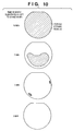
- Fig. 10 shows an observation result based on experiments about the relationship between the time in which the anodized substrate is left to stand in the air and the porous etching residue in the final process.
- epitaxial growth to 0.3 ⁇ m and oxidation of the epitaxial growth layer to 0.2 ⁇ m are performed.
- the substrate is cleaned and bonded to the a silicon substrate as the second substrate. After bonding, a heat treatment is performed at 1,100°C for 2 hrs.
- the porous layer side of the substrate is ground by a grinding apparatus called a backgrinder by about 615 ⁇ m, the porous silicon layer is exposed.
- the time in which the substrate is left to stand in the air after anodizing is 10, 7, 5, and 3 min from the upper side of the drawing.
- the hatchedportion indicates the porous layer residue which cannot be etched.
- the time in which the substrate is left to stand in the air after anodizing and the etching characteristics of the porous layer have a relationship.
- the time in which the substrate is left to stand is preferably as short as possible. In the actual process, however, a certain time need be taken into consideration. For example, an automatic anodizing apparatus must be designed in consideration of the water discharge and supply times, robot actuation time, and the like.
- the allowable time in which the substrate removed from the electrolyte is exposed to the air after anodizing is 3 min or less.
- an etching residue may be generated even in an air exposure time of 3 min.
- the time in which the substrate is left to stand in the air is preferably 2 min or less.
- the anodizing apparatus is an automatic apparatus having a substrate conveyor robot and the like and capable of anodizing a plurality of substrates at once in order to achieve the object of the present invention, i.e., mass-produce SOI substrates with uniform quality, as described above.
- the anodizing apparatus also has an arrangement for uniformly exposing all substrates to the air for 3 min or less from the end of anodizing to the start of cleaning with pure water.
- the number of substrates to be processed at once is most important in designing the apparatus. If a single substrate conveyor robot is used as the substrate conveyor robot, the number of substrates to be processed by the apparatus depends on the time required to transfer one substrate from the anodizing tank to the pure water rinse tank. Assume that the substrate transfer time is 20 sec per substrate. If conveyance of all substrates is complete within 3 min, the apparatus can process nine substrates at once.
- the discharge time must be taken into consideration. If the substrates are vertically held and processed in the anodizing tank, the upper portion of each substrate is exposed to the air first during discharge, and the lower portion is exposed to the air later. The reason why the discharge time poses a problem is that the reference must be set on the portion which is exposed to the air first. Assume that the discharge time of the apparatus having the robot is 40 sec. If the transfer time is 20 sec, only seven substrates can be transferred in 3 min. The apparatus can process only seven substrates at once.
- substrate transfer after anodizing may be omitted. That is, the electrolyte is discharged after anodizing, and pure water is supplied into the same tank to rinse the substrates. In this case, only the discharge time and supply time need be taken into consideration. For example, when the electrolyte is discharged in 40 sec, and water is supplied in 40 sec, the time in which the upper end portion of each substrate is exposed to the air is 3 min or less. Once the rinse with pure water is sufficiently performed, the substrate can be transferred to the drying stage or another cleaning stage in a longer time. In this case as well, the number of substrates to be processed is not limited basically.
- an anodizing apparatus having a full wafer conveyor robot as the substrate conveyor robot.
- this apparatus since all substrates are transferred at once independently of the number of substrates, the discharge time and transfer time of one cycle are taken into consideration.
- the advantage of a shorter process time of full transfer is also effective in the anodizing apparatus which can supply water to the same tank after discharge.
- full transfer can hardly be realized unless the substrate supporting method in the anodizing apparatus is sufficiently considered. The reason for this is as follows. Since anodizing is performed while completely sealing the substrate at the periphery and preventing current leakage, the seal interferes with the robot to set substrates in the holder or hold the substrates set in the holder at once.
- Figs. 2 to 4 show the holder, substrate conveyor robot, anodizing tank of an anodizing apparatus of the first embodiment, and an anodizing system using this apparatus.
- FIG. 2 is a schematic view of the substrate holding portion (to be referred to as a "holder” hereinafter) and substrate conveyor robot in the anodizing apparatus.
- a holder 102 has a circular opening portion 103 almost at the center of a rectangular plate, and an annular substrate chuck pad (to be referred to as a "pad” hereinafter) 104 is buried along the opening portion.
- a groove is formed in the pad surface, and the pressure in the groove can be reduced from the lower surface of the pad through an exhaust line 105.
- Reference numerals 106a and 106b denote substrate conveyor robots which are actuated in a pair.
- the robot 106a holds the lower surface of a substrate 101 by vacuum-chucking and moves it parallel and close to the surface of the holder 102. Subsequently, the robot 106b inserts its L-shaped portion into the opening portion 103 of the holder 102 and waits for the substrate 101.
- the robot 106b also has the vacuum-chucking function, like the robot 106a.
- the robot 106b When the lower surface of the substrate 101 comes into contact with the distal end of the robot 106b, the robot 106b chucks the substrate 101. The robot 106a cancels chucking and escapes upward.
- the robot 106b moves to the right side of the drawing, the lower surface of the substrate 101 comes into contact with the pad 104. Since the pressure in the groove of the pad 104 is reduced through the exhaust line 105, the substrate 101 is chucked on the pad 104. The robot 106b escapes upward through the opening portion 103. The substrate 101 is held by the holder 102 in the above manner. To release the substrate 101, an operation reverse to the above procedure is performed.
- Fig. 3 is a schematic sectional view of an anodizing apparatus having three holders shown in Fig. 2.
- a negative electrode 206a and positive electrode 206b are arranged at the two ends of an anodizing tank 210.
- the three holders 102 are sandwiched in tandem between the electrodes.
- Fig. 3 shows a state wherein the substrates 101 have already been held by the holders 102.
- the space between the electrode and the holder or between the holders is filled with an electrolyte 209 (more specifically, fluoric acid), so the chambers containing the electrolyte are isolated from each other by the substrates 101.
- Anodizing is performed by applying a DC voltage across the electrodes 206a and 206b in this state. After anodizing, the electrolyte 209 is discharged from a discharge port 208.
- Fig. 4 is a plan view of the anodizing system incorporating the above anodizing apparatus.
- the stage constituting the system has, from the left side, a loader 301, an anodizing tank 302, a washing tank 303, a robot drier 309, a spin drier 304, and an unloader 305.
- a single substrate conveyor robot 106 and a carrier conveyor robot 307 which have moving axes in the direction of alignment.
- the single substrate conveyor robot comprises the two portions 106a and 106b, as shown in Fig. 2.
- This system also has a system 308 for circulating and filtering the electrolyte in the anodizing tank.
- the carrier conveyor robot 307 moves the substrates from the washing tank 303 to the spin drier 304 together with the carrier, and then is dried by the robot drier 309 midway in returning to the washing tank 303.
- anodizing condition a mixed solution of fluoric acid and ethanol at 2 : 1 was used as the electrolyte.
- the current density in anodizing was 1 mA/cm 2 , and processing was performed for 11 min.
- the electrolyte was discharged in 30 sec using a discharge pump (not shown).
- the single substrate conveyor robot 106 sequentially transferred anodized substrates from a side close to the negative electrode to awafer carrier which had been set in the washing tank 303 in advance. Transfer of one substrate required 25 sec, and transfer of the second and third substrates required 23 sec and 21 sec, respectively.
- a time of 1 min and 39 sec was required until all the three substrates were transferred to the washing tank 303.
- a 0.3- ⁇ m thick single-crystal silicon layer was epitaxially grown on the porous silicon layer formed by the above process using a commercially available CVD apparatus.
- the surface of the epitaxial growth layer was anodized to 0.2 ⁇ m.
- This substrate and a silicon substrate which was prepared in advance were cleaned using a chemical solution of an acid and an alkali and bonded in a clean atmosphere.
- the bonded substrates were subjected to a heat treatment at 1,100°C in a nitrogen atmosphere for 2 hrs and integrated.
- the anodized side of the integrated substrates was ground using a backgrinder to remove the silicon substrate portion until the porous layer was exposed.
- the structure was dipped in a mixed solution of fluoric acid and hydrogen peroxide at 1 : 100 and left to stand for 2 hrs to remove the porous portion while leaving the epitaxial growth layer. The porous portion was completely removed, and the epitaxial silicon layer was exposed to the surface.
- the same holders and substrate conveyor robot as in the first embodiment are used.
- the number of holders increases from three in Fig. 3 to 25.
- discharge of the electrolyte after anodizing is omitted.
- the arm of a single substrate conveyor robot 106 is dipped in the electrolyte based on fluoric acid and an alcohol to directly remove the substrate from the solution.
- the time in which each substrate is exposed to the air corresponds to the conveyance time of the robot 106 from removal of the substrate from the electrolytic solution to dipping of the substrate in pure water in a washing tank 303.
- the material of the arm and substrate chuck portion of the robot 106 is limited to a material having HF resistance.
- a rod member of stainless steel with high rigidity which was inserted into a Teflon pipe (Teflon is the tradename of du Pont, U.S.A) was used as the arm of the robot.
- Teflon is the tradename of du Pont, U.S.A
- the chuck portion of a robot 106b (Fig. 2) consisted of a fluororubber.
- the 25 substrates transferred to the washing tank 303 were cleaned using pure water for 40 min after the last substrate was transferred to the washing tank 303.
- the subsequent processes were executed as in the first embodiment, and 25 SOI substrates with uniform quality without any porous layer residue were obtained, as in the first embodiment.
- the same holders and substrate conveyor robot as in the second embodiment are used. That is, 25 holders are used.
- the electrolyte is discharged after anodizing. Immediately after this, pure water is supplied into an anodizing tank 302 without transferring the substrates to a washing tank 303 and sufficiently cleaned in the anodizing tank 302.
- the time in which the 25 substrates are exposed to the air is about 30 sec for discharge of the electrolyte and about 40 sec for supply of pure water, i.e., a total of 1 min and 10 sec.
- the pure water rinse time in the anodizing tank 302 was about 40 min. After this, the pure water in the anodizing tank 302 was discharged, and the substrates were transferred to the washing tank 303 by a single substrate conveyor robot 106. Although a time of about 12 min is required to transfer all the 25 substrates from the anodizing tank to the washing tank 303, this poses no problem because most electrolyte in the pores in the porous layer is replaced with pure water.
- the 25 substrates transferred to the washing tank 303 were cleaned using pure water for 10 min after the last substrate was transferred to the washing tank 303.
- the subsequent processes were executed as in the first embodiment, and 25 SOI substrates with uniform quality without any porous layer residue were obtained, as in the first embodiment.
- the fourth embodiment uses the same apparatus arrangement as in the third embodiment, including the holder shape, the number of holders, and the substrate conveyor robot.
- the fourth embodiment is different from the third embodiment in that the electrolyte is not discharged after anodizing.
- pure water is supplied into the anodizing tank 302 without discharging the electrolyte, thereby replacing the electrolyte with pure water in the anodizing tank 302.
- the time in which the 25 substrates are exposed to the air is zero. In this case, however, the electrolyte is diluted and discarded, i.e., used for only one batch of anodizing. In addition, since the electrolyte is gradually diluted with pure water, a relatively long time is required until the electrolyte is completely replacedwith pure water.
- the pure water rinse time in the anodizing tank 302 was about 1 hr and 20 min. After this, the pure water in the anodizing tank 302 is discharged, and the substrates were transferred to a washing tank 303 by a single substrate conveyor robot 106. The 25 substrates transferred to the washing tank 303 are cleaned with pure water for 10 min after the last substrate was transferred to the washing tank 303. The subsequent processes were executed as in the first embodiment, and 25 SOI substrates with uniform quality without any porous layer residue were obtained, as in the first embodiment.
- the fifth embodiment uses the same apparatus arrangement as in the fourth embodiment, including the holder shape and the number of holders. However, the entire system including the substrate conveyance system is different.
- Fig. 5 is a schematic plan view showing an anodizing system of the fifth embodiment.
- Substrates are placed on a loader 401 while kept stored in a carrier.
- the loader 401 also functions as an unloader. From the carrier set at a predetermined position by the loader 401, the substrates were transferred to a boat 402 by the single substrate conveyor robot 408 one by one.
- the boat 402 has 25 grooves at a pitch of 25 mm.
- the 25 substrates are set in the boat 402 and then held by a full substrate conveyor robot 409a at once.
- Fig. 6 shows a specific shape of the robot 409a.
- the robot 409a has the same function as that of the substrate conveyor robot 106a shown in Fig. 2 except that one arm has a function of chucking 25 substrates.
- the 25 substrates are conveyed to an anodizing tank 403 while being held by the robot 409a.
- the substrates are set in holders by the same mechanism as in Fig. 2.
- a robot 409b as shown in Fig. 7, which has 25 robots 106b, is used.
- the 25 substrates are transferred to the full substrate conveyor robot 409a at once and set in the holders at once.
- the electrolyte is discharged in about 30 sec.
- the substrates are conveyed from the anodizing tank 403 to a washing tank 404 using the full substrate conveyor robots 409a and 409b again.
- a boat 405 having the same structure as that at the preceding stage of the anodizing apparatus is sank in the washing tank 404.
- the substrates are placed on this boat 405.
- the conveyance time is about 40 sec, or about 1 min and 10 sec when the discharge time after anodizing is added.
- the substrates are transferred to the boat 402 by the full substrate conveyor robot 409a again.
- the substrates are returned to the first carrier by the single substrate conveyor robot 408.
- the substrates stored in the carrier are conveyed to a spin drier 406 by a carrier conveyor robot 407, dried, and placed on the unloader 401.
- Each substrate having a porous layer which is obtained by the above operation, becomes an SOI substrate through the same processes as in the first embodiment.
- the method of separating the single-crystal silicon by rotating the Si water using water jet power is preferable for recycling purpose.
- the time in which the substrate removed from the electrolyte is exposed to-the air after anodizing is limited within a predetermined time. Subsequently, the substrate is rinsed with pure water to immediately dilute the electrolyte remaining in the pores in the porous layer and replace it with water.
- This method can be applied to the process of etching the porous layer while preventing any product difficult to etch from forming in the porous layer.
Landscapes
- Chemical & Material Sciences (AREA)
- Engineering & Computer Science (AREA)
- Chemical Kinetics & Catalysis (AREA)
- Electrochemistry (AREA)
- Materials Engineering (AREA)
- Metallurgy (AREA)
- Organic Chemistry (AREA)
- Weting (AREA)
Applications Claiming Priority (2)
| Application Number | Priority Date | Filing Date | Title |
|---|---|---|---|
| JP36101797 | 1997-12-26 | ||
| JP36101797A JP3501642B2 (ja) | 1997-12-26 | 1997-12-26 | 基板処理方法 |
Publications (2)
| Publication Number | Publication Date |
|---|---|
| EP0926712A2 true EP0926712A2 (de) | 1999-06-30 |
| EP0926712A3 EP0926712A3 (de) | 1999-09-08 |
Family
ID=18471844
Family Applications (1)
| Application Number | Title | Priority Date | Filing Date |
|---|---|---|---|
| EP98310477A Withdrawn EP0926712A3 (de) | 1997-12-26 | 1998-12-18 | SOI-Substrat Herstellungsverfahren und Vorrichtung |
Country Status (8)
| Country | Link |
|---|---|
| US (2) | US6200878B1 (de) |
| EP (1) | EP0926712A3 (de) |
| JP (1) | JP3501642B2 (de) |
| KR (1) | KR100363124B1 (de) |
| CN (1) | CN1127122C (de) |
| AU (1) | AU721781B2 (de) |
| SG (1) | SG70663A1 (de) |
| TW (1) | TW425628B (de) |
Cited By (1)
| Publication number | Priority date | Publication date | Assignee | Title |
|---|---|---|---|---|
| US8822305B2 (en) | 2007-09-21 | 2014-09-02 | Semiconductor Energy Laboratory Co., Ltd. | Substrate provided with semiconductor films and manufacturing method thereof |
Families Citing this family (220)
| Publication number | Priority date | Publication date | Assignee | Title |
|---|---|---|---|---|
| FR2773261B1 (fr) | 1997-12-30 | 2000-01-28 | Commissariat Energie Atomique | Procede pour le transfert d'un film mince comportant une etape de creation d'inclusions |
| US6417069B1 (en) * | 1999-03-25 | 2002-07-09 | Canon Kabushiki Kaisha | Substrate processing method and manufacturing method, and anodizing apparatus |
| US6664169B1 (en) | 1999-06-08 | 2003-12-16 | Canon Kabushiki Kaisha | Process for producing semiconductor member, process for producing solar cell, and anodizing apparatus |
| JP4108941B2 (ja) * | 2000-10-31 | 2008-06-25 | 株式会社荏原製作所 | 基板の把持装置、処理装置、及び把持方法 |
| US8507361B2 (en) * | 2000-11-27 | 2013-08-13 | Soitec | Fabrication of substrates with a useful layer of monocrystalline semiconductor material |
| US7101772B2 (en) * | 2000-12-30 | 2006-09-05 | Texas Instruments Incorporated | Means for forming SOI |
| KR100453454B1 (ko) * | 2001-01-09 | 2004-10-15 | 텔레포스 주식회사 | 양극화 반응 장치 및 단위 양극화 반응기 |
| FR2823599B1 (fr) | 2001-04-13 | 2004-12-17 | Commissariat Energie Atomique | Substrat demomtable a tenue mecanique controlee et procede de realisation |
| KR100476901B1 (ko) * | 2002-05-22 | 2005-03-17 | 삼성전자주식회사 | 소이 반도체기판의 형성방법 |
| US20040077140A1 (en) * | 2002-10-16 | 2004-04-22 | Andricacos Panayotis C. | Apparatus and method for forming uniformly thick anodized films on large substrates |
| FR2848336B1 (fr) * | 2002-12-09 | 2005-10-28 | Commissariat Energie Atomique | Procede de realisation d'une structure contrainte destinee a etre dissociee |
| FR2856844B1 (fr) * | 2003-06-24 | 2006-02-17 | Commissariat Energie Atomique | Circuit integre sur puce de hautes performances |
| FR2857953B1 (fr) | 2003-07-21 | 2006-01-13 | Commissariat Energie Atomique | Structure empilee, et procede pour la fabriquer |
| FR2861497B1 (fr) * | 2003-10-28 | 2006-02-10 | Soitec Silicon On Insulator | Procede de transfert catastrophique d'une couche fine apres co-implantation |
| US7256077B2 (en) * | 2004-05-21 | 2007-08-14 | Freescale Semiconductor, Inc. | Method for removing a semiconductor layer |
| US8399331B2 (en) | 2007-10-06 | 2013-03-19 | Solexel | Laser processing for high-efficiency thin crystalline silicon solar cell fabrication |
| US9508886B2 (en) | 2007-10-06 | 2016-11-29 | Solexel, Inc. | Method for making a crystalline silicon solar cell substrate utilizing flat top laser beam |
| KR101128725B1 (ko) * | 2005-06-30 | 2012-03-23 | 매그나칩 반도체 유한회사 | 반도체 장치의 제조방법 |
| FR2889887B1 (fr) * | 2005-08-16 | 2007-11-09 | Commissariat Energie Atomique | Procede de report d'une couche mince sur un support |
| CN100391826C (zh) * | 2005-09-09 | 2008-06-04 | 华东师范大学 | 一种硅的微通道制作方法 |
| FR2891281B1 (fr) | 2005-09-28 | 2007-12-28 | Commissariat Energie Atomique | Procede de fabrication d'un element en couches minces. |
| CN100365454C (zh) * | 2005-11-14 | 2008-01-30 | 浙江大学 | 用于纳米光子技术的聚合物上硅纳米膜制备方法 |
| US8035027B2 (en) | 2006-10-09 | 2011-10-11 | Solexel, Inc. | Solar module structures and assembly methods for pyramidal three-dimensional thin-film solar cells |
| US8193076B2 (en) | 2006-10-09 | 2012-06-05 | Solexel, Inc. | Method for releasing a thin semiconductor substrate from a reusable template |
| US8035028B2 (en) * | 2006-10-09 | 2011-10-11 | Solexel, Inc. | Pyramidal three-dimensional thin-film solar cells |
| US20080264477A1 (en) * | 2006-10-09 | 2008-10-30 | Soltaix, Inc. | Methods for manufacturing three-dimensional thin-film solar cells |
| US7999174B2 (en) * | 2006-10-09 | 2011-08-16 | Solexel, Inc. | Solar module structures and assembly methods for three-dimensional thin-film solar cells |
| FR2910179B1 (fr) * | 2006-12-19 | 2009-03-13 | Commissariat Energie Atomique | PROCEDE DE FABRICATION DE COUCHES MINCES DE GaN PAR IMPLANTATION ET RECYCLAGE D'UN SUBSTRAT DE DEPART |
| FR2922359B1 (fr) * | 2007-10-12 | 2009-12-18 | Commissariat Energie Atomique | Procede de fabrication d'une structure micro-electronique impliquant un collage moleculaire |
| FR2925221B1 (fr) * | 2007-12-17 | 2010-02-19 | Commissariat Energie Atomique | Procede de transfert d'une couche mince |
| US8030119B2 (en) * | 2008-03-08 | 2011-10-04 | Crystal Solar, Inc. | Integrated method and system for manufacturing monolithic panels of crystalline solar cells |
| US8294026B2 (en) * | 2008-11-13 | 2012-10-23 | Solexel, Inc. | High-efficiency thin-film solar cells |
| US9076642B2 (en) | 2009-01-15 | 2015-07-07 | Solexel, Inc. | High-Throughput batch porous silicon manufacturing equipment design and processing methods |
| US8906218B2 (en) | 2010-05-05 | 2014-12-09 | Solexel, Inc. | Apparatus and methods for uniformly forming porous semiconductor on a substrate |
| US9318644B2 (en) | 2009-05-05 | 2016-04-19 | Solexel, Inc. | Ion implantation and annealing for thin film crystalline solar cells |
| EP2427914A4 (de) * | 2009-05-05 | 2013-06-05 | Solexel Inc | Hochproduktionsanlage zur herstellung poröser halbleiter |
| FR2947098A1 (fr) * | 2009-06-18 | 2010-12-24 | Commissariat Energie Atomique | Procede de transfert d'une couche mince sur un substrat cible ayant un coefficient de dilatation thermique different de celui de la couche mince |
| US12027518B1 (en) | 2009-10-12 | 2024-07-02 | Monolithic 3D Inc. | 3D semiconductor devices and structures with metal layers |
| US11984445B2 (en) | 2009-10-12 | 2024-05-14 | Monolithic 3D Inc. | 3D semiconductor devices and structures with metal layers |
| US10910364B2 (en) | 2009-10-12 | 2021-02-02 | Monolitaic 3D Inc. | 3D semiconductor device |
| US10354995B2 (en) | 2009-10-12 | 2019-07-16 | Monolithic 3D Inc. | Semiconductor memory device and structure |
| US10366970B2 (en) | 2009-10-12 | 2019-07-30 | Monolithic 3D Inc. | 3D semiconductor device and structure |
| US11374118B2 (en) | 2009-10-12 | 2022-06-28 | Monolithic 3D Inc. | Method to form a 3D integrated circuit |
| US10388863B2 (en) | 2009-10-12 | 2019-08-20 | Monolithic 3D Inc. | 3D memory device and structure |
| US10043781B2 (en) | 2009-10-12 | 2018-08-07 | Monolithic 3D Inc. | 3D semiconductor device and structure |
| US10157909B2 (en) | 2009-10-12 | 2018-12-18 | Monolithic 3D Inc. | 3D semiconductor device and structure |
| US11018133B2 (en) | 2009-10-12 | 2021-05-25 | Monolithic 3D Inc. | 3D integrated circuit |
| MY166305A (en) | 2009-12-09 | 2018-06-25 | Solexel Inc | High-efficiency photovoltaic back-contact solar cell structures and manufacturing methods using thin planar semiconductor absorbers |
| WO2011100647A2 (en) | 2010-02-12 | 2011-08-18 | Solexel, Inc. | Double-sided reusable template for fabrication of semiconductor substrates for photovoltaic cell and microelectronics device manufacturing |
| US9870937B2 (en) | 2010-06-09 | 2018-01-16 | Ob Realty, Llc | High productivity deposition reactor comprising a gas flow chamber having a tapered gas flow space |
| US10217667B2 (en) | 2011-06-28 | 2019-02-26 | Monolithic 3D Inc. | 3D semiconductor device, fabrication method and system |
| EP2601687A4 (de) | 2010-08-05 | 2018-03-07 | Solexel, Inc. | Rückseitenverstärkung und vernetzungsmittel für solarzellen |
| US11482440B2 (en) | 2010-12-16 | 2022-10-25 | Monolithic 3D Inc. | 3D semiconductor device and structure with a built-in test circuit for repairing faulty circuits |
| US10497713B2 (en) | 2010-11-18 | 2019-12-03 | Monolithic 3D Inc. | 3D semiconductor memory device and structure |
| US12362219B2 (en) | 2010-11-18 | 2025-07-15 | Monolithic 3D Inc. | 3D semiconductor memory device and structure |
| US11600667B1 (en) | 2010-10-11 | 2023-03-07 | Monolithic 3D Inc. | Method to produce 3D semiconductor devices and structures with memory |
| US11018191B1 (en) | 2010-10-11 | 2021-05-25 | Monolithic 3D Inc. | 3D semiconductor device and structure |
| US11315980B1 (en) | 2010-10-11 | 2022-04-26 | Monolithic 3D Inc. | 3D semiconductor device and structure with transistors |
| US11469271B2 (en) | 2010-10-11 | 2022-10-11 | Monolithic 3D Inc. | Method to produce 3D semiconductor devices and structures with memory |
| US11257867B1 (en) | 2010-10-11 | 2022-02-22 | Monolithic 3D Inc. | 3D semiconductor device and structure with oxide bonds |
| US11024673B1 (en) | 2010-10-11 | 2021-06-01 | Monolithic 3D Inc. | 3D semiconductor device and structure |
| US11227897B2 (en) | 2010-10-11 | 2022-01-18 | Monolithic 3D Inc. | Method for producing a 3D semiconductor memory device and structure |
| US10290682B2 (en) | 2010-10-11 | 2019-05-14 | Monolithic 3D Inc. | 3D IC semiconductor device and structure with stacked memory |
| US11158674B2 (en) | 2010-10-11 | 2021-10-26 | Monolithic 3D Inc. | Method to produce a 3D semiconductor device and structure |
| US10896931B1 (en) | 2010-10-11 | 2021-01-19 | Monolithic 3D Inc. | 3D semiconductor device and structure |
| US11327227B2 (en) | 2010-10-13 | 2022-05-10 | Monolithic 3D Inc. | Multilevel semiconductor device and structure with electromagnetic modulators |
| US11605663B2 (en) | 2010-10-13 | 2023-03-14 | Monolithic 3D Inc. | Multilevel semiconductor device and structure with image sensors and wafer bonding |
| US11855100B2 (en) | 2010-10-13 | 2023-12-26 | Monolithic 3D Inc. | Multilevel semiconductor device and structure with oxide bonding |
| US11404466B2 (en) | 2010-10-13 | 2022-08-02 | Monolithic 3D Inc. | Multilevel semiconductor device and structure with image sensors |
| US11164898B2 (en) | 2010-10-13 | 2021-11-02 | Monolithic 3D Inc. | Multilevel semiconductor device and structure |
| US11133344B2 (en) | 2010-10-13 | 2021-09-28 | Monolithic 3D Inc. | Multilevel semiconductor device and structure with image sensors |
| US11694922B2 (en) | 2010-10-13 | 2023-07-04 | Monolithic 3D Inc. | Multilevel semiconductor device and structure with oxide bonding |
| US10978501B1 (en) | 2010-10-13 | 2021-04-13 | Monolithic 3D Inc. | Multilevel semiconductor device and structure with waveguides |
| US12360310B2 (en) | 2010-10-13 | 2025-07-15 | Monolithic 3D Inc. | Multilevel semiconductor device and structure with oxide bonding |
| US11855114B2 (en) | 2010-10-13 | 2023-12-26 | Monolithic 3D Inc. | Multilevel semiconductor device and structure with image sensors and wafer bonding |
| US10679977B2 (en) | 2010-10-13 | 2020-06-09 | Monolithic 3D Inc. | 3D microdisplay device and structure |
| US11929372B2 (en) | 2010-10-13 | 2024-03-12 | Monolithic 3D Inc. | Multilevel semiconductor device and structure with image sensors and wafer bonding |
| US10943934B2 (en) | 2010-10-13 | 2021-03-09 | Monolithic 3D Inc. | Multilevel semiconductor device and structure |
| US11869915B2 (en) | 2010-10-13 | 2024-01-09 | Monolithic 3D Inc. | Multilevel semiconductor device and structure with image sensors and wafer bonding |
| US12094892B2 (en) | 2010-10-13 | 2024-09-17 | Monolithic 3D Inc. | 3D micro display device and structure |
| US12080743B2 (en) | 2010-10-13 | 2024-09-03 | Monolithic 3D Inc. | Multilevel semiconductor device and structure with image sensors and wafer bonding |
| US11984438B2 (en) | 2010-10-13 | 2024-05-14 | Monolithic 3D Inc. | Multilevel semiconductor device and structure with oxide bonding |
| US11063071B1 (en) | 2010-10-13 | 2021-07-13 | Monolithic 3D Inc. | Multilevel semiconductor device and structure with waveguides |
| US11437368B2 (en) | 2010-10-13 | 2022-09-06 | Monolithic 3D Inc. | Multilevel semiconductor device and structure with oxide bonding |
| US10998374B1 (en) | 2010-10-13 | 2021-05-04 | Monolithic 3D Inc. | Multilevel semiconductor device and structure |
| US11163112B2 (en) | 2010-10-13 | 2021-11-02 | Monolithic 3D Inc. | Multilevel semiconductor device and structure with electromagnetic modulators |
| US10833108B2 (en) | 2010-10-13 | 2020-11-10 | Monolithic 3D Inc. | 3D microdisplay device and structure |
| US11043523B1 (en) | 2010-10-13 | 2021-06-22 | Monolithic 3D Inc. | Multilevel semiconductor device and structure with image sensors |
| US12136562B2 (en) | 2010-11-18 | 2024-11-05 | Monolithic 3D Inc. | 3D semiconductor device and structure with single-crystal layers |
| US11495484B2 (en) | 2010-11-18 | 2022-11-08 | Monolithic 3D Inc. | 3D semiconductor devices and structures with at least two single-crystal layers |
| US11923230B1 (en) | 2010-11-18 | 2024-03-05 | Monolithic 3D Inc. | 3D semiconductor device and structure with bonding |
| US11355380B2 (en) | 2010-11-18 | 2022-06-07 | Monolithic 3D Inc. | Methods for producing 3D semiconductor memory device and structure utilizing alignment marks |
| US11443971B2 (en) | 2010-11-18 | 2022-09-13 | Monolithic 3D Inc. | 3D semiconductor device and structure with memory |
| US11862503B2 (en) | 2010-11-18 | 2024-01-02 | Monolithic 3D Inc. | Method for producing a 3D semiconductor device and structure with memory cells and multiple metal layers |
| US11121021B2 (en) | 2010-11-18 | 2021-09-14 | Monolithic 3D Inc. | 3D semiconductor device and structure |
| US12243765B2 (en) | 2010-11-18 | 2025-03-04 | Monolithic 3D Inc. | 3D semiconductor device and structure with metal layers and memory cells |
| US11615977B2 (en) | 2010-11-18 | 2023-03-28 | Monolithic 3D Inc. | 3D semiconductor memory device and structure |
| US11211279B2 (en) | 2010-11-18 | 2021-12-28 | Monolithic 3D Inc. | Method for processing a 3D integrated circuit and structure |
| US12154817B1 (en) | 2010-11-18 | 2024-11-26 | Monolithic 3D Inc. | Methods for producing a 3D semiconductor memory device and structure |
| US12100611B2 (en) | 2010-11-18 | 2024-09-24 | Monolithic 3D Inc. | Methods for producing a 3D semiconductor device and structure with memory cells and multiple metal layers |
| US11482439B2 (en) | 2010-11-18 | 2022-10-25 | Monolithic 3D Inc. | Methods for producing a 3D semiconductor memory device comprising charge trap junction-less transistors |
| US11031275B2 (en) | 2010-11-18 | 2021-06-08 | Monolithic 3D Inc. | 3D semiconductor device and structure with memory |
| US12144190B2 (en) | 2010-11-18 | 2024-11-12 | Monolithic 3D Inc. | 3D semiconductor device and structure with bonding and memory cells preliminary class |
| US11854857B1 (en) | 2010-11-18 | 2023-12-26 | Monolithic 3D Inc. | Methods for producing a 3D semiconductor device and structure with memory cells and multiple metal layers |
| US12272586B2 (en) | 2010-11-18 | 2025-04-08 | Monolithic 3D Inc. | 3D semiconductor memory device and structure with memory and metal layers |
| US11004719B1 (en) | 2010-11-18 | 2021-05-11 | Monolithic 3D Inc. | Methods for producing a 3D semiconductor memory device and structure |
| US12033884B2 (en) | 2010-11-18 | 2024-07-09 | Monolithic 3D Inc. | Methods for producing a 3D semiconductor device and structure with memory cells and multiple metal layers |
| US11355381B2 (en) | 2010-11-18 | 2022-06-07 | Monolithic 3D Inc. | 3D semiconductor memory device and structure |
| US11735462B2 (en) | 2010-11-18 | 2023-08-22 | Monolithic 3D Inc. | 3D semiconductor device and structure with single-crystal layers |
| US11804396B2 (en) | 2010-11-18 | 2023-10-31 | Monolithic 3D Inc. | Methods for producing a 3D semiconductor device and structure with memory cells and multiple metal layers |
| US11521888B2 (en) | 2010-11-18 | 2022-12-06 | Monolithic 3D Inc. | 3D semiconductor device and structure with high-k metal gate transistors |
| US11610802B2 (en) | 2010-11-18 | 2023-03-21 | Monolithic 3D Inc. | Method for producing a 3D semiconductor device and structure with single crystal transistors and metal gate electrodes |
| US11901210B2 (en) | 2010-11-18 | 2024-02-13 | Monolithic 3D Inc. | 3D semiconductor device and structure with memory |
| US12125737B1 (en) | 2010-11-18 | 2024-10-22 | Monolithic 3D Inc. | 3D semiconductor device and structure with metal layers and memory cells |
| US11482438B2 (en) | 2010-11-18 | 2022-10-25 | Monolithic 3D Inc. | Methods for producing a 3D semiconductor memory device and structure |
| US11569117B2 (en) | 2010-11-18 | 2023-01-31 | Monolithic 3D Inc. | 3D semiconductor device and structure with single-crystal layers |
| US12068187B2 (en) | 2010-11-18 | 2024-08-20 | Monolithic 3D Inc. | 3D semiconductor device and structure with bonding and DRAM memory cells |
| US11018042B1 (en) | 2010-11-18 | 2021-05-25 | Monolithic 3D Inc. | 3D semiconductor memory device and structure |
| US11164770B1 (en) | 2010-11-18 | 2021-11-02 | Monolithic 3D Inc. | Method for producing a 3D semiconductor memory device and structure |
| US11094576B1 (en) | 2010-11-18 | 2021-08-17 | Monolithic 3D Inc. | Methods for producing a 3D semiconductor memory device and structure |
| US11107721B2 (en) | 2010-11-18 | 2021-08-31 | Monolithic 3D Inc. | 3D semiconductor device and structure with NAND logic |
| US11508605B2 (en) | 2010-11-18 | 2022-11-22 | Monolithic 3D Inc. | 3D semiconductor memory device and structure |
| US11784082B2 (en) | 2010-11-18 | 2023-10-10 | Monolithic 3D Inc. | 3D semiconductor device and structure with bonding |
| US12463076B2 (en) | 2010-12-16 | 2025-11-04 | Monolithic 3D Inc. | 3D semiconductor device and structure |
| EP2710639A4 (de) | 2011-05-20 | 2015-11-25 | Solexel Inc | Selbstaktivierte vorderseiten-vorspannung für eine solarzelle |
| US10388568B2 (en) | 2011-06-28 | 2019-08-20 | Monolithic 3D Inc. | 3D semiconductor device and system |
| US11881443B2 (en) | 2012-04-09 | 2024-01-23 | Monolithic 3D Inc. | 3D semiconductor device and structure with metal layers and a connective path |
| US11164811B2 (en) | 2012-04-09 | 2021-11-02 | Monolithic 3D Inc. | 3D semiconductor device with isolation layers and oxide-to-oxide bonding |
| US11088050B2 (en) | 2012-04-09 | 2021-08-10 | Monolithic 3D Inc. | 3D semiconductor device with isolation layers |
| US11476181B1 (en) | 2012-04-09 | 2022-10-18 | Monolithic 3D Inc. | 3D semiconductor device and structure with metal layers |
| US11410912B2 (en) | 2012-04-09 | 2022-08-09 | Monolithic 3D Inc. | 3D semiconductor device with vias and isolation layers |
| US11616004B1 (en) | 2012-04-09 | 2023-03-28 | Monolithic 3D Inc. | 3D semiconductor device and structure with metal layers and a connective path |
| US11694944B1 (en) | 2012-04-09 | 2023-07-04 | Monolithic 3D Inc. | 3D semiconductor device and structure with metal layers and a connective path |
| US11735501B1 (en) | 2012-04-09 | 2023-08-22 | Monolithic 3D Inc. | 3D semiconductor device and structure with metal layers and a connective path |
| US11594473B2 (en) | 2012-04-09 | 2023-02-28 | Monolithic 3D Inc. | 3D semiconductor device and structure with metal layers and a connective path |
| US10600888B2 (en) | 2012-04-09 | 2020-03-24 | Monolithic 3D Inc. | 3D semiconductor device |
| US11063024B1 (en) | 2012-12-22 | 2021-07-13 | Monlithic 3D Inc. | Method to form a 3D semiconductor device and structure |
| US12051674B2 (en) | 2012-12-22 | 2024-07-30 | Monolithic 3D Inc. | 3D semiconductor device and structure with metal layers |
| US11018116B2 (en) | 2012-12-22 | 2021-05-25 | Monolithic 3D Inc. | Method to form a 3D semiconductor device and structure |
| US11309292B2 (en) | 2012-12-22 | 2022-04-19 | Monolithic 3D Inc. | 3D semiconductor device and structure with metal layers |
| US11916045B2 (en) | 2012-12-22 | 2024-02-27 | Monolithic 3D Inc. | 3D semiconductor device and structure with metal layers |
| US11217565B2 (en) | 2012-12-22 | 2022-01-04 | Monolithic 3D Inc. | Method to form a 3D semiconductor device and structure |
| US11967583B2 (en) | 2012-12-22 | 2024-04-23 | Monolithic 3D Inc. | 3D semiconductor device and structure with metal layers |
| US11961827B1 (en) | 2012-12-22 | 2024-04-16 | Monolithic 3D Inc. | 3D semiconductor device and structure with metal layers |
| US11784169B2 (en) | 2012-12-22 | 2023-10-10 | Monolithic 3D Inc. | 3D semiconductor device and structure with metal layers |
| US10651054B2 (en) | 2012-12-29 | 2020-05-12 | Monolithic 3D Inc. | 3D semiconductor device and structure |
| US10600657B2 (en) | 2012-12-29 | 2020-03-24 | Monolithic 3D Inc | 3D semiconductor device and structure |
| US10903089B1 (en) | 2012-12-29 | 2021-01-26 | Monolithic 3D Inc. | 3D semiconductor device and structure |
| US11177140B2 (en) | 2012-12-29 | 2021-11-16 | Monolithic 3D Inc. | 3D semiconductor device and structure |
| US10115663B2 (en) | 2012-12-29 | 2018-10-30 | Monolithic 3D Inc. | 3D semiconductor device and structure |
| US11087995B1 (en) | 2012-12-29 | 2021-08-10 | Monolithic 3D Inc. | 3D semiconductor device and structure |
| US12249538B2 (en) | 2012-12-29 | 2025-03-11 | Monolithic 3D Inc. | 3D semiconductor device and structure including power distribution grids |
| US11430667B2 (en) | 2012-12-29 | 2022-08-30 | Monolithic 3D Inc. | 3D semiconductor device and structure with bonding |
| US11430668B2 (en) | 2012-12-29 | 2022-08-30 | Monolithic 3D Inc. | 3D semiconductor device and structure with bonding |
| US10892169B2 (en) | 2012-12-29 | 2021-01-12 | Monolithic 3D Inc. | 3D semiconductor device and structure |
| US11004694B1 (en) | 2012-12-29 | 2021-05-11 | Monolithic 3D Inc. | 3D semiconductor device and structure |
| FR3002219B1 (fr) | 2013-02-19 | 2015-04-10 | Commissariat Energie Atomique | Procede de fabrication d'une structure micromecanique et/ou nanomecanique comportant une surface poreuse |
| US12094965B2 (en) | 2013-03-11 | 2024-09-17 | Monolithic 3D Inc. | 3D semiconductor device and structure with metal layers and memory cells |
| US11869965B2 (en) | 2013-03-11 | 2024-01-09 | Monolithic 3D Inc. | 3D semiconductor device and structure with metal layers and memory cells |
| US11935949B1 (en) | 2013-03-11 | 2024-03-19 | Monolithic 3D Inc. | 3D semiconductor device and structure with metal layers and memory cells |
| US8902663B1 (en) | 2013-03-11 | 2014-12-02 | Monolithic 3D Inc. | Method of maintaining a memory state |
| US10325651B2 (en) | 2013-03-11 | 2019-06-18 | Monolithic 3D Inc. | 3D semiconductor device with stacked memory |
| US11088130B2 (en) | 2014-01-28 | 2021-08-10 | Monolithic 3D Inc. | 3D semiconductor device and structure |
| US10840239B2 (en) | 2014-08-26 | 2020-11-17 | Monolithic 3D Inc. | 3D semiconductor device and structure |
| US12100646B2 (en) | 2013-03-12 | 2024-09-24 | Monolithic 3D Inc. | 3D semiconductor device and structure with metal layers |
| US11923374B2 (en) | 2013-03-12 | 2024-03-05 | Monolithic 3D Inc. | 3D semiconductor device and structure with metal layers |
| US11398569B2 (en) | 2013-03-12 | 2022-07-26 | Monolithic 3D Inc. | 3D semiconductor device and structure |
| US10224279B2 (en) | 2013-03-15 | 2019-03-05 | Monolithic 3D Inc. | Semiconductor device and structure |
| US11487928B2 (en) | 2013-04-15 | 2022-11-01 | Monolithic 3D Inc. | Automation for monolithic 3D devices |
| US9021414B1 (en) | 2013-04-15 | 2015-04-28 | Monolithic 3D Inc. | Automation for monolithic 3D devices |
| US11720736B2 (en) | 2013-04-15 | 2023-08-08 | Monolithic 3D Inc. | Automation methods for 3D integrated circuits and devices |
| US11341309B1 (en) | 2013-04-15 | 2022-05-24 | Monolithic 3D Inc. | Automation for monolithic 3D devices |
| US11574109B1 (en) | 2013-04-15 | 2023-02-07 | Monolithic 3D Inc | Automation methods for 3D integrated circuits and devices |
| US11030371B2 (en) | 2013-04-15 | 2021-06-08 | Monolithic 3D Inc. | Automation for monolithic 3D devices |
| US11270055B1 (en) | 2013-04-15 | 2022-03-08 | Monolithic 3D Inc. | Automation for monolithic 3D devices |
| FR3011835B1 (fr) | 2013-10-16 | 2015-12-25 | Commissariat Energie Atomique | Procede de realisation par voie electrochimique d'au moins une zone poreuse d'une structure micro et/ou nanoelectronique |
| RU2554298C1 (ru) * | 2013-12-05 | 2015-06-27 | Федеральное государственное бюджетное учреждение науки Омский научный центр Сибирского отделения Российской академии наук (ОНЦ СО РАН) | Способ получения многослойной структуры пористый кремний на изоляторе |
| US10297586B2 (en) | 2015-03-09 | 2019-05-21 | Monolithic 3D Inc. | Methods for processing a 3D semiconductor device |
| US11107808B1 (en) | 2014-01-28 | 2021-08-31 | Monolithic 3D Inc. | 3D semiconductor device and structure |
| US11031394B1 (en) | 2014-01-28 | 2021-06-08 | Monolithic 3D Inc. | 3D semiconductor device and structure |
| US12094829B2 (en) | 2014-01-28 | 2024-09-17 | Monolithic 3D Inc. | 3D semiconductor device and structure |
| US12477752B2 (en) | 2015-09-21 | 2025-11-18 | Monolithic 3D Inc. | 3D semiconductor memory devices and structures |
| US12016181B2 (en) | 2015-10-24 | 2024-06-18 | Monolithic 3D Inc. | 3D semiconductor device and structure with logic and memory |
| US12219769B2 (en) | 2015-10-24 | 2025-02-04 | Monolithic 3D Inc. | 3D semiconductor device and structure with logic and memory |
| US12035531B2 (en) | 2015-10-24 | 2024-07-09 | Monolithic 3D Inc. | 3D semiconductor device and structure with logic and memory |
| US11296115B1 (en) | 2015-10-24 | 2022-04-05 | Monolithic 3D Inc. | 3D semiconductor device and structure |
| US11937422B2 (en) | 2015-11-07 | 2024-03-19 | Monolithic 3D Inc. | Semiconductor memory device and structure |
| US11011507B1 (en) | 2015-04-19 | 2021-05-18 | Monolithic 3D Inc. | 3D semiconductor device and structure |
| US11114464B2 (en) | 2015-10-24 | 2021-09-07 | Monolithic 3D Inc. | 3D semiconductor device and structure |
| US10418369B2 (en) | 2015-10-24 | 2019-09-17 | Monolithic 3D Inc. | Multi-level semiconductor memory device and structure |
| US11056468B1 (en) | 2015-04-19 | 2021-07-06 | Monolithic 3D Inc. | 3D semiconductor device and structure |
| US10825779B2 (en) | 2015-04-19 | 2020-11-03 | Monolithic 3D Inc. | 3D semiconductor device and structure |
| US10847540B2 (en) | 2015-10-24 | 2020-11-24 | Monolithic 3D Inc. | 3D semiconductor memory device and structure |
| US11114427B2 (en) | 2015-11-07 | 2021-09-07 | Monolithic 3D Inc. | 3D semiconductor processor and memory device and structure |
| US12615784B2 (en) | 2015-11-07 | 2026-04-28 | Monolithic 3D Inc. | 3D semiconductor memory device and structure |
| US11978731B2 (en) | 2015-09-21 | 2024-05-07 | Monolithic 3D Inc. | Method to produce a multi-level semiconductor memory device and structure |
| US10381328B2 (en) | 2015-04-19 | 2019-08-13 | Monolithic 3D Inc. | Semiconductor device and structure |
| US11956952B2 (en) | 2015-08-23 | 2024-04-09 | Monolithic 3D Inc. | Semiconductor memory device and structure |
| US12250830B2 (en) | 2015-09-21 | 2025-03-11 | Monolithic 3D Inc. | 3D semiconductor memory devices and structures |
| US12100658B2 (en) | 2015-09-21 | 2024-09-24 | Monolithic 3D Inc. | Method to produce a 3D multilayer semiconductor device and structure |
| US12178055B2 (en) | 2015-09-21 | 2024-12-24 | Monolithic 3D Inc. | 3D semiconductor memory devices and structures |
| DE112016004265T5 (de) | 2015-09-21 | 2018-06-07 | Monolithic 3D Inc. | 3d halbleitervorrichtung und -struktur |
| US10522225B1 (en) | 2015-10-02 | 2019-12-31 | Monolithic 3D Inc. | Semiconductor device with non-volatile memory |
| US11991884B1 (en) | 2015-10-24 | 2024-05-21 | Monolithic 3D Inc. | 3D semiconductor device and structure with logic and memory |
| US12120880B1 (en) | 2015-10-24 | 2024-10-15 | Monolithic 3D Inc. | 3D semiconductor device and structure with logic and memory |
| US20180068886A1 (en) * | 2016-09-02 | 2018-03-08 | Qualcomm Incorporated | Porous semiconductor layer transfer for an integrated circuit structure |
| US11711928B2 (en) | 2016-10-10 | 2023-07-25 | Monolithic 3D Inc. | 3D memory devices and structures with control circuits |
| US11329059B1 (en) | 2016-10-10 | 2022-05-10 | Monolithic 3D Inc. | 3D memory devices and structures with thinned single crystal substrates |
| US12225704B2 (en) | 2016-10-10 | 2025-02-11 | Monolithic 3D Inc. | 3D memory devices and structures with memory arrays and metal layers |
| US11869591B2 (en) | 2016-10-10 | 2024-01-09 | Monolithic 3D Inc. | 3D memory devices and structures with control circuits |
| US11812620B2 (en) | 2016-10-10 | 2023-11-07 | Monolithic 3D Inc. | 3D DRAM memory devices and structures with control circuits |
| US11930648B1 (en) | 2016-10-10 | 2024-03-12 | Monolithic 3D Inc. | 3D memory devices and structures with metal layers |
| US11251149B2 (en) | 2016-10-10 | 2022-02-15 | Monolithic 3D Inc. | 3D memory device and structure |
| JP6911812B2 (ja) * | 2018-06-06 | 2021-07-28 | 信越半導体株式会社 | 陽極酸化装置、陽極酸化方法及び陽極酸化装置の陰極の製造方法 |
| US11296106B2 (en) | 2019-04-08 | 2022-04-05 | Monolithic 3D Inc. | 3D memory semiconductor devices and structures |
| US11018156B2 (en) | 2019-04-08 | 2021-05-25 | Monolithic 3D Inc. | 3D memory semiconductor devices and structures |
| US11158652B1 (en) | 2019-04-08 | 2021-10-26 | Monolithic 3D Inc. | 3D memory semiconductor devices and structures |
| US10892016B1 (en) | 2019-04-08 | 2021-01-12 | Monolithic 3D Inc. | 3D memory semiconductor devices and structures |
| US11763864B2 (en) | 2019-04-08 | 2023-09-19 | Monolithic 3D Inc. | 3D memory semiconductor devices and structures with bit-line pillars |
| KR102834667B1 (ko) * | 2021-11-19 | 2025-07-17 | 한국과학기술원 | 단결정 박막의 전사방법 및 이를 이용한 반도체 소자의 제조방법 |
Family Cites Families (17)
| Publication number | Priority date | Publication date | Assignee | Title |
|---|---|---|---|---|
| US5750000A (en) * | 1990-08-03 | 1998-05-12 | Canon Kabushiki Kaisha | Semiconductor member, and process for preparing same and semiconductor device formed by use of same |
| SG59963A1 (en) * | 1990-08-03 | 1999-02-22 | Canon Kk | Semiconductor member and process for preparing semiconductor member |
| CA2069038C (en) * | 1991-05-22 | 1997-08-12 | Kiyofumi Sakaguchi | Method for preparing semiconductor member |
| SU1829751A1 (ru) * | 1991-06-17 | 1996-08-27 | Институт микроэлектроники АН СССР | Способ изготовления чувствительного элемента полупроводникового газового сенсора |
| TW211621B (de) * | 1991-07-31 | 1993-08-21 | Canon Kk | |
| JP3112106B2 (ja) * | 1991-10-11 | 2000-11-27 | キヤノン株式会社 | 半導体基材の作製方法 |
| DE69233314T2 (de) * | 1991-10-11 | 2005-03-24 | Canon K.K. | Verfahren zur Herstellung von Halbleiter-Produkten |
| JPH05198556A (ja) | 1992-01-23 | 1993-08-06 | Canon Inc | 陽極化成装置 |
| JP3214631B2 (ja) | 1992-01-31 | 2001-10-02 | キヤノン株式会社 | 半導体基体及びその作製方法 |
| JP3191972B2 (ja) * | 1992-01-31 | 2001-07-23 | キヤノン株式会社 | 半導体基板の作製方法及び半導体基板 |
| JP3237888B2 (ja) * | 1992-01-31 | 2001-12-10 | キヤノン株式会社 | 半導体基体及びその作製方法 |
| JP3416163B2 (ja) * | 1992-01-31 | 2003-06-16 | キヤノン株式会社 | 半導体基板及びその作製方法 |
| JPH06244389A (ja) | 1992-12-25 | 1994-09-02 | Canon Inc | 半導体基板の作製方法及び該方法により作製された半導体基板 |
| JP3257580B2 (ja) * | 1994-03-10 | 2002-02-18 | キヤノン株式会社 | 半導体基板の作製方法 |
| KR0171067B1 (ko) * | 1994-12-05 | 1999-03-30 | 문정환 | 단결정 soi웨이퍼 제조방법 |
| EP0755068B1 (de) | 1995-07-21 | 2003-06-04 | Canon Kabushiki Kaisha | Halbleitendes Substrat und dessen Herstellungsverfahren |
| JP3376258B2 (ja) | 1996-11-28 | 2003-02-10 | キヤノン株式会社 | 陽極化成装置及びそれに関連する装置及び方法 |
-
1997
- 1997-12-26 JP JP36101797A patent/JP3501642B2/ja not_active Expired - Fee Related
-
1998
- 1998-12-15 SG SG1998005837A patent/SG70663A1/en unknown
- 1998-12-15 US US09/211,570 patent/US6200878B1/en not_active Expired - Lifetime
- 1998-12-16 TW TW087120964A patent/TW425628B/zh not_active IP Right Cessation
- 1998-12-18 EP EP98310477A patent/EP0926712A3/de not_active Withdrawn
- 1998-12-24 AU AU98179/98A patent/AU721781B2/en not_active Ceased
- 1998-12-25 CN CN98126345A patent/CN1127122C/zh not_active Expired - Fee Related
- 1998-12-26 KR KR10-1998-0058987A patent/KR100363124B1/ko not_active Expired - Fee Related
-
2000
- 2000-10-05 US US09/680,376 patent/US6428620B1/en not_active Expired - Lifetime
Cited By (1)
| Publication number | Priority date | Publication date | Assignee | Title |
|---|---|---|---|---|
| US8822305B2 (en) | 2007-09-21 | 2014-09-02 | Semiconductor Energy Laboratory Co., Ltd. | Substrate provided with semiconductor films and manufacturing method thereof |
Also Published As
| Publication number | Publication date |
|---|---|
| US6428620B1 (en) | 2002-08-06 |
| KR19990063515A (ko) | 1999-07-26 |
| AU9817998A (en) | 1999-07-15 |
| KR100363124B1 (ko) | 2003-01-24 |
| JPH11195773A (ja) | 1999-07-21 |
| AU721781B2 (en) | 2000-07-13 |
| US6200878B1 (en) | 2001-03-13 |
| TW425628B (en) | 2001-03-11 |
| JP3501642B2 (ja) | 2004-03-02 |
| CN1127122C (zh) | 2003-11-05 |
| EP0926712A3 (de) | 1999-09-08 |
| CN1221207A (zh) | 1999-06-30 |
| SG70663A1 (en) | 2000-02-22 |
Similar Documents
| Publication | Publication Date | Title |
|---|---|---|
| US6428620B1 (en) | Substrate processing method and apparatus and SOI substrate | |
| KR100415513B1 (ko) | 양극화성방법 및 양극화성장치와 반도체기판의 제조방법 | |
| US6517697B1 (en) | Anodizing method | |
| KR100385255B1 (ko) | 다공질체의 세정방법 및 다공질체, 비다공질막 및 접합기판의 제작방법 | |
| US6653209B1 (en) | Method of producing silicon thin film, method of constructing SOI substrate and semiconductor device | |
| EP1026729A2 (de) | Verbundbauteil und zugehöriges Trennverfahren, Stapel aus gebondeten Substraten und zugehöriges Trennverfahren, Transferverfahren für Transferschicht, und Herstellungsverfahren für ein SOI Substrat | |
| EP0603849B1 (de) | Verfahren zur Herstellung eines Halbleitersubstrates mittels eines Verbundverfahrens | |
| US6417069B1 (en) | Substrate processing method and manufacturing method, and anodizing apparatus | |
| US20040152319A1 (en) | Processing apparatus for processing substrate by process solution | |
| AU741464B2 (en) | Anodizing apparatus and method and porous substrate | |
| JP4598413B2 (ja) | 貼り合わせウエーハの製造方法及び貼り合わせウエーハの酸化膜除去用治具 | |
| JPH1197654A (ja) | 半導体基板の製造方法 | |
| JP3320379B2 (ja) | 貼り合わせ基板の作製方法 | |
| JP2000336499A (ja) | 基板の処理方法及び製造方法並びに陽極化成装置 | |
| JP2000133558A (ja) | 半導体基体の作製方法およびそれにより作製された基体 | |
| JP2004266072A (ja) | 基板搬送装置 | |
| JP2004099965A (ja) | 陽極化成装置及び陽極化成方法、基板製造方法、並びに、基板処理装置及び基板処理方法 | |
| JP2007194346A (ja) | 半導体作製方法およびその製造装置 |
Legal Events
| Date | Code | Title | Description |
|---|---|---|---|
| PUAI | Public reference made under article 153(3) epc to a published international application that has entered the european phase |
Free format text: ORIGINAL CODE: 0009012 |
|
| AK | Designated contracting states |
Kind code of ref document: A2 Designated state(s): AT BE DE ES FR GB IT NL SE |
|
| AX | Request for extension of the european patent |
Free format text: AL;LT;LV;MK;RO;SI |
|
| PUAL | Search report despatched |
Free format text: ORIGINAL CODE: 0009013 |
|
| AK | Designated contracting states |
Kind code of ref document: A3 Designated state(s): AT BE CH CY DE DK ES FI FR GB GR IE IT LI LU MC NL PT SE |
|
| AX | Request for extension of the european patent |
Free format text: AL;LT;LV;MK;RO;SI |
|
| RIC1 | Information provided on ipc code assigned before grant |
Free format text: 6H 01L 21/306 A, 6C 25D 11/18 B, 6H 01L 21/00 B, 6H 01L 21/762 B, 6H 01L 21/20 B |
|
| 17P | Request for examination filed |
Effective date: 20000121 |
|
| AKX | Designation fees paid |
Free format text: AT BE DE ES FR GB IT NL SE |
|
| 17Q | First examination report despatched |
Effective date: 20021023 |
|
| STAA | Information on the status of an ep patent application or granted ep patent |
Free format text: STATUS: THE APPLICATION HAS BEEN WITHDRAWN |
|
| 18W | Application withdrawn |
Effective date: 20040726 |