EP0926742B1 - Méthode de fabrication d'un difsposif récepteur de lumière - Google Patents
Méthode de fabrication d'un difsposif récepteur de lumière Download PDFInfo
- Publication number
- EP0926742B1 EP0926742B1 EP99200499A EP99200499A EP0926742B1 EP 0926742 B1 EP0926742 B1 EP 0926742B1 EP 99200499 A EP99200499 A EP 99200499A EP 99200499 A EP99200499 A EP 99200499A EP 0926742 B1 EP0926742 B1 EP 0926742B1
- Authority
- EP
- European Patent Office
- Prior art keywords
- photo
- electrodes
- light
- receiving device
- electrically conductive
- Prior art date
- Legal status (The legal status is an assumption and is not a legal conclusion. Google has not performed a legal analysis and makes no representation as to the accuracy of the status listed.)
- Expired - Lifetime
Links
Images


Classifications
-
- H—ELECTRICITY
- H10—SEMICONDUCTOR DEVICES; ELECTRIC SOLID-STATE DEVICES NOT OTHERWISE PROVIDED FOR
- H10F—INORGANIC SEMICONDUCTOR DEVICES SENSITIVE TO INFRARED RADIATION, LIGHT, ELECTROMAGNETIC RADIATION OF SHORTER WAVELENGTH OR CORPUSCULAR RADIATION
- H10F30/00—Individual radiation-sensitive semiconductor devices in which radiation controls the flow of current through the devices, e.g. photodetectors
- H10F30/20—Individual radiation-sensitive semiconductor devices in which radiation controls the flow of current through the devices, e.g. photodetectors the devices having potential barriers, e.g. phototransistors
- H10F30/21—Individual radiation-sensitive semiconductor devices in which radiation controls the flow of current through the devices, e.g. photodetectors the devices having potential barriers, e.g. phototransistors the devices being sensitive to infrared, visible or ultraviolet radiation
- H10F30/22—Individual radiation-sensitive semiconductor devices in which radiation controls the flow of current through the devices, e.g. photodetectors the devices having potential barriers, e.g. phototransistors the devices being sensitive to infrared, visible or ultraviolet radiation the devices having only one potential barrier, e.g. photodiodes
- H10F30/227—Individual radiation-sensitive semiconductor devices in which radiation controls the flow of current through the devices, e.g. photodetectors the devices having potential barriers, e.g. phototransistors the devices being sensitive to infrared, visible or ultraviolet radiation the devices having only one potential barrier, e.g. photodiodes the potential barrier being a Schottky barrier
-
- H—ELECTRICITY
- H10—SEMICONDUCTOR DEVICES; ELECTRIC SOLID-STATE DEVICES NOT OTHERWISE PROVIDED FOR
- H10F—INORGANIC SEMICONDUCTOR DEVICES SENSITIVE TO INFRARED RADIATION, LIGHT, ELECTROMAGNETIC RADIATION OF SHORTER WAVELENGTH OR CORPUSCULAR RADIATION
- H10F77/00—Constructional details of devices covered by this subclass
- H10F77/40—Optical elements or arrangements
- H10F77/413—Optical elements or arrangements directly associated or integrated with the devices, e.g. back reflectors
Definitions
- the present invention relates to a method of fabricating a photo-receiving device.
- photoelectric conversion refers to the function of converting a light signal to an electrical signal in a photo-receiving device.
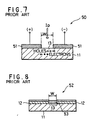
- Figure 7 illustrates the structure of a conventional photo-receiving device 50 as described in the IEEE Journal of Quantum Electronics (Vol. 28, pp. 2358-2368, 1992) for converting light signals to electrical signals at a relatively high speed.
- the photo-receiving device 50 comprises a substrate 11 that constitutes the photoelectric conversion portion (which can also be referred to as a light-absorbing portion, as this is a photo-receiving device), and a pair of opposed electrode portions 51, each in the form of a thin film of metal, formed on the surface of the substrate 11.
- the exposed surface of the substrate 11 between the electrodes 51 forms an optical window 13 for the entry of the light Ip to be detected.
- excited carriers (electrons and holes) are generated in the substrate 11. Holes, shown in the drawing as blank circles, are drawn to the electrode 51 with the relatively negative (-) potential, and electrons, shown as solid circles, are drawn to the electrode 51 with the relatively positive (+) potential, setting up a flow of a photoelectric current (photo detection current) which takes place via the electrodes 51, whereby the incidence of the light Ip is detected.
- photoelectric current photo detection current
- the width W of the optical window 13 that is, the smaller the distance between the electrodes 51, the faster the operating speed of the device is, and raising the applied voltage increases device speed and sensitivity. Also, making the width W of the optical window 13 no larger than the wavelength of the light Ip to be detected imparts an evanescent field to the light Ip impinging on the light-absorbing substrate 11 and causes the incident light Ip to be absorbed in the vicinity of the surface of the substrate 11.
- the excited carriers generated in the vicinity of the surface of the substrate 11 are drawn rapidly to the electrodes 51, enabling higher speed operation to be achieved and the affect of carrier recombination to be reduced.
- a first problem is that, since the optical window 13 on the surface of the substrate 11 between the electrodes 51 is exposed, applying a higher voltage across the electrodes 51 giving rise to creeping discharge along the exposed surface of the optical window 13 and air-gap discharge, rendering the device unusable. That is, if the width W between the electrodes 51 is reduced beyond a certain limit, even a low voltage causes a dielectric breakdown. On the other hand, even in cases where the width W of the incident light window 13 can be increased, within the limitation that it does not exceed the wavelength of the incident light I P , there are major constraints on the voltage that can be applied.
- a second problem is that of the limits of the process technology. Even with existing electron beam lithography, a relatively high precision fine pattern process technology, an electrode gap cannot really be precision-fabricated to a width W of 100 nm or less, and even 300 nm or less is quite difficult.
- a conventional method of resolving the first problem is to cover, or bury, the exposed surface portion constituting the optical window 13 between the electrodes 51.
- This will now be described, with reference to Figure 8.
- the following description is not limited to photo-receiving devices, being also applicable to devices, such as light emitting devices, having a light emitting area defined in the form of an optical window.
- reference numeral 52 is used to denote the photo-device shown in Figure 8, the light-absorbing portion 11 of Figure 7 is the photoelectric conversion portion in the general meaning of the term, and the term metallic film electrodes 51 is encompassed by the term optically nontransparent conductive film (electrodes) 12.
- To fabricate the photo-device 52 existing lithographic technology is used to remove a prescribed region of an optically nontransparent conductive film 12 formed on photoelectric conversion portion 11, thereby exposing a defined portion that forms an optical window 13.
- Non-uniformities in the thickness of the surface deposition film gives rise to variation in device characteristics, and high frequency characteristics can be degraded by dielectric deposits.
- a very fine optical window is used, forming a high-quality insulative film over the window that has high dielectric resistance is difficult.
- US-A-3949463 describes the formation of an optical window by a process which involves four steps. These are (1) patterning by photoresist, (2) metal deposition, (3) removal of photoresist and (4) anodization. The process suffers from the constraints relating to optical window width referred to above.
- An object of the present invention is to provide a method of fabricating a photo-receiving device that enables the above-described drawbacks to be resolved or alleviated and an optical window to be formed to have a smaller width than that of conventional photo-devices.
- a method of fabricating a photo-receiving device comprising the steps of forming an optically non-transparent, electrically conductive layer on a surface of a photoelectric conversion substrate, oxidising a portion of said optically non-transparent, electrically conductive layer to form in said layer a transparent or semi-transparent protective insulation structure of a prescribed width and length thereby defining an optical window characterised in that the oxidation is effected with an atomic force microscope.
- the optically nontransparent, electrically conductive layer may be of a metal or an alloy, or a semiconductor (including semi-insulators), or may include a semiconductor superlattice structure.
- a photo-device is fabricated to have a prescribed area on a surface of the photo-receiving photoelectric conversion substrate forming an optical window of a prescribed width via which light is received or emitted.
- it is a photo-device that requires that an optical nontransparent, electrically conductive layer be formed at each side of the optical window, the defined optical window region and an insulation structure for protecting the arrangement that may be used to vary the optical properties of the optical guide.
- the insulation creepage distance between the electrodes is increased by making the thickness of the optical guide greater than the thickness of the electrodes.
- the photo-receiving device has a plurality of optical guides arranged in parallel between the pair of electrodes, and means each provided between adjacent optical guides so as not to transmit the light to be detected.
- a method of fabricating a photo-device comprising a step of forming an optically nontransparent, electrically conductive layer on a surface of a photoelectric conversion substrate, and a step whereby a portion of the optically nontransparent, electrically conductive layer is transformed to form over the optical window a light-permeable protective insulation structure of a prescribed width and length, and at the same time define an optical window region on the substrate surface beneath the protective insulation structure.
- the optically nontransparent, electrically conductive layer may be of a metal or an alloy, or a semiconductor (including semi-insulators), or may include a semiconductor superlattice structure.
- a photo-device is fabricated to have a prescribed area on a surface of the photo-receiving or photoemitting photoelectric conversion substrate forming an optical window of a prescribed width via which light is received or emitted.
- it is a photo-device that requires that an optically nontransparent, electrically conductive layer be formed at each side of the optical window, the defined optical window region and an insulation structure for protecting the optical window can be formed in a single step. This is highly efficient and eliminates the need to use a costly vacuum vapor deposition apparatus to form the protective layer over the entire surface.
- the optically nontransparent, electrically conductive layer is transformed by oxidation.
- This oxidation is effected using a scanning probe apparatus.
- a fine optical window having a width that does not exceed the wavelength of the light to be detected, and a high-quality, highly dielectrically-resistant protective insulative structure for the optical window can both be formed by the same step.
- carrier speed is increased by applying a high field strength while the effect of carrier recombination is decreased, thus providing a photo-device that is faster and more sensitive.
- the photoelectric conversion substrate is of a light-absorbing material having a light receiving function, a non-transformed portion of the optically nontransparent, electrically conductive layer functions as an electrode to apply a voltage to the light-absorbing substrate, and the protective insulation structure functions as an optical guide that directs light to the substrate.
- the thickness of the protective insulation structure preferably is thicker than the thickness of the non-transformed portions of the optically nontransparent, electrically conductive layer at each side, and when said portions of the layer remaining at each side are utilized as a pair of electrodes, the insulation creepage distance between the electrodes is increased, thereby increasing the resistance to dielectric breakdown.
- Figure 1 shows an example of basic steps or processes used to fabricate a photo-device according to the method of the invention.
- parts corresponding to parts in the conventional devices 50 and 52 of Figures 7 and 8,already described, are given the same reference numerals.
- Figure 1 (A) shows a conductive, optically nontransparent film layer 12 formed on a surface of a light receiving photoelectric conversion substrate 11.
- the internal constitution of the substrate 11 is not specifically defined by the invention, and may be comprised in accordance with existing device structural principles. If the device is formed as a conventional MSM photo-receiving device, as described in the foregoing, the substrate 11 will function as a light-absorber, and in terms of material, will be formed of a bulk semiconductor such as GaAs.
- the film 12 may be formed of a suitable metal (including alloys) or semiconductor, including a semiconductor having a superlattice structure.
- a material that is at least non-permeable, or has very low permeability, to the light to be detected, in the case of a photo-receiving device, and has significant electrical conductivity can be regarded as being applicable for the purpose of the invention.
- STM scanning tunneling microscope
- AFM atomic force microscope
- the present inventors were able to form a titanium oxide line with a minimum width of 18 nm by oxidizing a titanium layer deposited on a GaAs substrate. The same result was also obtained with an AFM. While not directly related to this invention, with an AFM the target film does not have to be electrically conductive.
- a light-permeable protective insulation structure 15 having a prescribed width and length is formed to protect the optical window, and the same formation process is used to define a region for the optical window 13 on the substrate surface beneath the structure 15, as shown in Figure 1 (C) .
- the remaining nontransformed portions of the optically nontransparent conductive film 12 at each side of the protective insulation structure 15 can be used as electrodes. Since in such a case the insulation structure 15 is disposed between the electrodes 12, the insulation creepage distance is increased, enhancing the resistance to dielectric breakdown. Increasing the thickness of the structure 15 to above a certain level also enhances insulation capabilities.
- FIG. 2 is a cross-sectional view of a photo-receiving device 10A.
- the photo-receiving device 10A comprises a light-absorbing substrate 11 of GaAs or other such suitable semiconductor on which a pair of electrodes 12 is formed, with the space between the electrodes 12 forming an optical window 13 for light entry.
- the electrodes 12 are usually of titanium or other such metal, but can also be formed of silicon or another such semiconductor which has been made conductive by the introduction of an appropriate impurity.
- the light-absorbing substrate 11 can be used as the structural substrate of the photo-receiving device 10A, this is not limitative, as the illustrated structure can be formed using a physical support substrate other than the one shown.
- the optical window 13 is in the form of a portion of the surface exposed to the air.
- the optical window portion of the photo-receiving device 10A is provided with a protective insulation structure formed of a suitable insulation material such as titanium oxide, silicon oxide or silicon nitride.
- this structure 15 also serves as an optical guide.
- This optical guide 15 needs to at least be light-permeable, that is, transparent or semitransparent with respect to the light I P to be detected. The above are examples of materials that can be treated as transparent to light of most wavelengths.
- the portion of the substrate 11 between the electrodes is not exposed, it eliminates or alleviates the surface discharge on the exposed surface of the substrate window 13 that is a problem with the conventional arrangement, and, using the same width W between electrodes 12 as a conventional configuration, enables a higher voltage to be applied. It is desirable to make the thickness t of the optical guide 15 greater than the thickness of the electrodes 12. Doing this increases the creeping distance between the electrodes 12 by an amount corresponding to the increase in thickness, thus providing adequate resistance to the type of air gap discharge across the electrodes 12 to which the conventional device arrangement is prone.
- the width W of the optical window 13 is made to not exceed the wavelength of the light I P to be detected, the light I P impinging on the light-absorbing substrate 11 appears as an evanescent photoelectric field, the photoelectric field strength is increased just in the vicinity of the surface of the substrate 11 and the incident light I P is absorbed in said vicinity of the substrate 11 surface.
- the inventive photo-receiving device 10A Since in the inventive photo-receiving device 10A a higher voltage can be applied across the electrodes 12 than in a conventional device, and the electrical field strength is therefore higher at the surface than inside the substrate, excited carriers (electrons and holes) generated by the incident light I P in the vicinity of the surface of the substrate 11, close to the electrodes 12, are drawn at high speed to the respective electrode (the relatively positive electrode in the case of electrons, and relatively negative electrode in the case of holes). In other words, photoelectric conversion (photodetection) can be effected at a higher speed. Moreover, the high speed at which the carriers are drawn away as a result of the high voltage applied means that less recombination takes place, which helps to increase the sensitivity and output of the device.
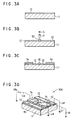
- Figure 3 shows more details of the process used to fabricate the MSM photo-receiving device 10A of Figure 2 according to the method of this invention.
- a full-surface conductive layer 12 of titanium is deposited on a GaAs semiconductor substrate 11.
- a STM probe P is positioned near a prescribed surface portion of the titanium layer 12, as shown in Figure 3 (B), and a potential of 5 V is applied between the probe P and the layer 12 under atmospheric conditions (that is, in an environment that includes moisture), setting up a tunneling current, while at the same time the probe is scanned in a direction S normal to the drawing sheet.
- the scanning speed is set to produce a titanium oxide line 15' having a width of 100 nm.
- mounting electrodes 14 of Ti/Au are formed at a desired portion on the electrodes 12 to facilitate a connection to an external circuit that may be required.
- ground electrodes 14' of Ti/Au are formed parallel to a stripe that includes electrodes 12 and optical guide 15. In this example, stripes are each 5 ⁇ m wide and are 5 ⁇ m apart. This enables a bias line Lb that applies a bias voltage Vb to be connected to one of the electrodes 12, and a signal line Lr to a resistance load R to be connected to the other electrode 12, and a ground line Le to be connected to each of the ground electrodes 14' forming a shield structure.
- the measurement system shown in Figure 4 was used to evaluate the thus-fabricated photo-receiving device 10A, using the electro-optical sampling method.
- This is a method in which polarization changes in a laser beam corresponding to changes in the electrical field of an electro-optical crystal disposed on the circuit to be measured are detected, producing an electrical signal that is measured at a time resolution in the femtosecond range.
- the light source was a colliding pulse mode-locked (CPM) dye laser 22, fed by an argon ion laser 21, with an output of around 10 mW, an output pulse width of 40 fs, and a wavelength of 620 nm.
- CCM colliding pulse mode-locked
- the titanium oxide optical guide 15 of the photo-receiving device 10A exhibited adequate transparency to this light of wavelength 620 nm, and satisfactory electrical insulation properties.
- the beam from the CPM dye laser 22 is split by a 9:1 beam splitter 23 into an exciting beam Ip and a sampling beam Is, respectively.
- the exciting beam Ip is passed through a variable delay apparatus 32 to adjust the difference with respect to the light path of the sampling beam Is, and is then directed into the optical guide 15 of the photo-receiving device 10A.
- the sampling beam Is is passed through a half-wave plate 24 and polarizer 25 to adjust the polarization direction, and then into an electro-optical (EO) probe 31.
- EO electro-optical
- the EO probe 31 is a LiTaO 3 plate 300 ⁇ m long, 250 ⁇ m wide and 50 ⁇ m thick, with an electro-optical coefficient of 35.8 pm/V, and has a multilayer, dielectric antireflection coating on the rear surface of the crystal in contact with the photo-receiving device.
- the crystal orientation of the EO probe 31 and the polarization direction of the sampling beam Is are set for optimum sensitivity with respect to an electrical field perpendicular to the stripe.
- the reflected sampling beam Is phase modulated by electrical field permeation into the EO probe 31 is subjected to phase compensation by a Babinet-Soleil compensator 26, deflected by a polarizing beam splitter 27 and intensity modulated by a pair of photoreceivers 28a and 28b.
- the outputs of the photoreceivers 28a and 28b are passed through a differential amplifier 29 to a lock-in amplifier 34 and thereby locked in to the same 1 MHz that is applied to the fabricated device by a signal generator 33.
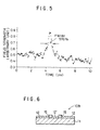
- Figure 5 displays a plot of the measurement results based on the output of the lock-in amplifier 34.
- the vertical axis is field strength and the horizontal axis is time.
- the device fabrication of this invention makes it possible to define the region for the optical window 13 and to form the protective insulation structure (optical guide) 15 for the optical window 13 in a single process.
- the optical window 13 enables the optical window 13 to be formed to a width as fine as around 100 nm, so it does not exceed the wavelength of the light to be detected, and the formation of a protective insulation structure 15 that exhibits high quality and high dielectric resistance.
- Applying the method to the fabrication of an MSM photo-receiving device results in a device that combines high speed with high sensitivity.
- the width W of the optical window 13 is no larger than the wavelength of the light to be detected, the light I P impinging on the light-absorbing substrate 11 appears as an evanescent photoelectric field, the photoelectric field strength is increased just in the vicinity of the surface of the substrate 11 and the incident light is absorbed in this substrate 11 surface vicinity.
- the photo-receiving device 10A is provided with the high quality protective insulation structure 15, with its high dielectric resistance, compared to a conventional device a higher voltage can be applied across the electrodes 12, and the electrical field strength is therefore higher at the surface than inside the substrate, excited carriers (electrons and holes) generated by the incident light I P in the vicinity of the surface of the substrate 11, close to the electrodes 12, are drawn at high speed to the respective electrode (the relatively positive electrode in the case of electrons, and relatively negative electrode in the case of holes). In other words, photoelectric conversion (photodetection) can be effected at a higher speed.
- the high speed at which the carriers are drawn away as a result of the high voltage applied means that less recombination takes place, which helps to increase the sensitivity and output power of the device.
- This invention provides a device that is faster and more sensitive than a conventional device. This is because even if, in the device of this invention, the width W of the gap between the electrodes 12 is increased to more than the 300 nm of a conventional device, while observing the provision that the width W does not exceed the wavelength of the light to be detected, the lower risk of a dielectric breakdown occurring means that a higher voltage can be applied across the electrodes 12. Doing this would ease the fabrication process burden.
- An example is the above-described processing method in which a scanning probe apparatus is applied to the formation of the protective insulation structure 15; for example, forming an oxide line of a desired width by oscillating the probe P to each side of the scan line, as described above.
- a different existing fine pattern process technology such as electron beam lithography or selective epitaxis.
- the protective insulation structure/optical guide 15 does not have to be an insulator. It is only required that it be located between the electrodes 12 and exhibit higher resistance than that of the substrate 11, and as such may be formed of a semiconductor based on an insulation material. If GaAs is used for the substrate 11, for light-permeability (minimal photo-absorption) the structure 15 could be formed of AlAs. GaP or other such semiconductor having a larger band-gap than that of the GaAs. However, when such a semiconductor is used to form the optical guide 15, to ensure complete insulation a small gap should be left between the guide 15 and at least one of the electrodes 12 and this gap filled with an insulation material. This corresponds to an embodiment in which the optical guide 15 is constituted of materials having different properties.
- Figure 6 shows an embodiment of a photo-receiving device 10B in which the optical window is provided with two or more discernible optical guides 15 (only two are shown in the drawing), and a nontransparent interstitial portion or means 12' is provided between adjacent guides 15.
- the detection sensitivity can be increased by the number of optical guides 15 having a width not exceeding the wavelength of the light to be detected.
- the interstitial means 12' may be conductive or insulative, but preferably are conductive, since that enables them to be formed of the same material as the film used to form the electrodes 12 at each side. Any desired fine pattern process technology may be used to form the optical guides 15.
- a scanning probe based process is highly rational, as it enables the process used to form che guides 15 to be utilized to also form the electrodes 12 and interstitial means 12', all at the same time.
- the optical guides 15 may be formed of a mixed multiplicity of materials having different properties, such as insulators and semiconductors, as long as this does not depart from the defined scope of the invention.
- the optical guides 15 may include a structure that enables the optical properties of the guides to be varied.
Landscapes
- Light Receiving Elements (AREA)
Claims (5)
- Procédé de fabrication d'un dispositif photorécepteur comprenant les étapes consistant à :former une couche (12) électriquement conductrice, optiquement non-transparente, sur une surface d'un substrat de conversion photo-électrique (11),oxyder une partie de ladite couche (12) électriquement conductrice, optiquement non-transparente, afin de former dans ladite couche (12) une structure d'isolation et de protection transparente ou semi-transparente (15), ayant une largeur et une longueur prescrites, ce qui permet ainsi de définir une fenêtre optique (13)caractérisé en ce que
l'oxydation est réalisée à l'aide d'un microscope à force atomique. - Procédé de fabrication, selon la revendication 1, dans lequel la couche (12) électriquement conductrice, optiquement non-transparente est un métal ou un alliage.
- Procédé de fabrication, selon la revendication 1, dans lequel la couche (12) électriquement conductrice, optiquement non-transparente est un semiconducteur.
- Procédé de fabrication, selon la revendication 1, caractérisé en ce que la partie de la couche (12) électriquement conductrice, optiquement non-transparente, qui est soumise à l'oxydation est transformée, sur ladite couche, en emplacements multiples qui sont séparés les uns des autres.
- Procédé de fabrication, selon la revendication 1, caractérisé en ce que les parties non-oxydées de la couche (12) électriquement conductrice, optiquement non-transparente jouent le rôle d'électrodes servant à appliquer une tension sur le substrat de conversion photo-électrique (11), et que la structure d'isolation et de protection transparente ou semi-transparente (15) joue le rôle de guide optique servant à diriger de la lumière dans le substrat de conversion photo-électrique (11).
Applications Claiming Priority (5)
| Application Number | Priority Date | Filing Date | Title |
|---|---|---|---|
| JP808295 | 1995-01-23 | ||
| JP808395 | 1995-01-23 | ||
| JP7008083A JP2705757B2 (ja) | 1995-01-23 | 1995-01-23 | 受光素子 |
| JP808295A JP2666888B2 (ja) | 1995-01-23 | 1995-01-23 | 光素子の製造方法 |
| EP96300405A EP0723302B1 (fr) | 1995-01-23 | 1996-01-22 | Dispositif récepteur de lumière |
Related Parent Applications (1)
| Application Number | Title | Priority Date | Filing Date |
|---|---|---|---|
| EP96300405A Division EP0723302B1 (fr) | 1995-01-23 | 1996-01-22 | Dispositif récepteur de lumière |
Publications (3)
| Publication Number | Publication Date |
|---|---|
| EP0926742A2 EP0926742A2 (fr) | 1999-06-30 |
| EP0926742A3 EP0926742A3 (fr) | 1999-09-01 |
| EP0926742B1 true EP0926742B1 (fr) | 2006-04-05 |
Family
ID=26342522
Family Applications (2)
| Application Number | Title | Priority Date | Filing Date |
|---|---|---|---|
| EP99200499A Expired - Lifetime EP0926742B1 (fr) | 1995-01-23 | 1996-01-22 | Méthode de fabrication d'un difsposif récepteur de lumière |
| EP96300405A Expired - Lifetime EP0723302B1 (fr) | 1995-01-23 | 1996-01-22 | Dispositif récepteur de lumière |
Family Applications After (1)
| Application Number | Title | Priority Date | Filing Date |
|---|---|---|---|
| EP96300405A Expired - Lifetime EP0723302B1 (fr) | 1995-01-23 | 1996-01-22 | Dispositif récepteur de lumière |
Country Status (3)
| Country | Link |
|---|---|
| US (3) | US5661328A (fr) |
| EP (2) | EP0926742B1 (fr) |
| DE (2) | DE69614583T2 (fr) |
Families Citing this family (24)
| Publication number | Priority date | Publication date | Assignee | Title |
|---|---|---|---|---|
| DE19737498C2 (de) * | 1997-08-28 | 2002-09-12 | Deutsche Telekom Ag | Optische Verbindung |
| FR2803950B1 (fr) * | 2000-01-14 | 2002-03-01 | Centre Nat Rech Scient | Dispositif de photodetection a microresonateur metal- semiconducteur vertical et procede de fabrication de ce dispositif |
| US6445021B1 (en) * | 2000-09-20 | 2002-09-03 | International Business Machines Corporation | Negative differential resistance reoxidized nitride silicon-based photodiode and method |
| US6403990B1 (en) * | 2001-03-27 | 2002-06-11 | Agilent Technologies, Inc. | Short turn-off time photoconductive switch |
| US7110629B2 (en) * | 2002-07-22 | 2006-09-19 | Applied Materials, Inc. | Optical ready substrates |
| US7072534B2 (en) * | 2002-07-22 | 2006-07-04 | Applied Materials, Inc. | Optical ready substrates |
| US7043106B2 (en) * | 2002-07-22 | 2006-05-09 | Applied Materials, Inc. | Optical ready wafers |
| FR2842945B1 (fr) * | 2002-07-25 | 2005-11-11 | Centre Nat Rech Scient | Dispositif de photodetection de type msm et a cavite resonnante comprenant un miroir a reseau d'electrodes metalliques |
| WO2005001520A2 (fr) * | 2003-05-29 | 2005-01-06 | Applied Materials, Inc. | Acheminement en serie de signaux optiques |
| EP1649566A4 (fr) * | 2003-06-27 | 2007-08-15 | Applied Materials Inc | Systeme laser a points quantiques pulses presentant faible une instabilite |
| US20050016446A1 (en) | 2003-07-23 | 2005-01-27 | Abbott John S. | CaF2 lenses with reduced birefringence |
| JP5094385B2 (ja) * | 2004-03-22 | 2012-12-12 | リサーチ ファウンデーション オブ ザ シティー ユニバーシティ オブ ニューヨーク | 高応答性高帯域金属−半導体−金属光電デバイス |
| US7272273B2 (en) * | 2005-01-21 | 2007-09-18 | Neophotonics Corporation | Photodetector coupled to a planar waveguide |
| US20060222024A1 (en) * | 2005-03-15 | 2006-10-05 | Gray Allen L | Mode-locked semiconductor lasers with quantum-confined active region |
| US20060227825A1 (en) * | 2005-04-07 | 2006-10-12 | Nl-Nanosemiconductor Gmbh | Mode-locked quantum dot laser with controllable gain properties by multiple stacking |
| WO2007027615A1 (fr) * | 2005-09-01 | 2007-03-08 | Applied Materials, Inc. | Technique d'arete pour la fabrication d'un capteur optique et d'un guide d'ondes optique |
| WO2007065614A2 (fr) * | 2005-12-07 | 2007-06-14 | Innolume Gmbh | Source laser avec emission a spectre a large bande |
| US7835408B2 (en) | 2005-12-07 | 2010-11-16 | Innolume Gmbh | Optical transmission system |
| US7561607B2 (en) * | 2005-12-07 | 2009-07-14 | Innolume Gmbh | Laser source with broadband spectrum emission |
| KR20090050696A (ko) * | 2007-11-16 | 2009-05-20 | 삼성전기주식회사 | 광배선 기판 및 그 제조방법 |
| WO2010065731A2 (fr) * | 2008-12-03 | 2010-06-10 | Innolume Gmbh | Laser à semi-conducteurs à faible intensité relative de bruit de modes longitudinaux individuels et système de transmission optique incorporant le laser |
| US8860078B2 (en) | 2012-05-14 | 2014-10-14 | The Johns Hopkins University | Simplified devices utilizing novel pn-semiconductor structures |
| CA2873703A1 (fr) * | 2012-05-14 | 2013-11-21 | The Johns Hopkins University | Dispositif simplifie utilisant de nouvelles structures semi-conductrices pn |
| US8785855B2 (en) * | 2012-10-16 | 2014-07-22 | Uvic Industry Partnerships Inc. | Interlaced terahertz transceiver using plasmonic resonance |
Citations (1)
| Publication number | Priority date | Publication date | Assignee | Title |
|---|---|---|---|---|
| US3949463A (en) * | 1973-02-13 | 1976-04-13 | Communications Satellite Corporation (Comsat) | Method of applying an anti-reflective coating to a solar cell |
Family Cites Families (4)
| Publication number | Priority date | Publication date | Assignee | Title |
|---|---|---|---|---|
| DE1299087B (de) * | 1966-05-10 | 1969-07-10 | Siemens Ag | Feldeffekt-Fototransistor |
| JPS6386481A (ja) * | 1986-09-30 | 1988-04-16 | Agency Of Ind Science & Technol | 高感度横型受光素子 |
| JPS63229867A (ja) * | 1987-03-11 | 1988-09-26 | ハネウエル・インコーポレーテツド | チヤネル導波路形シヨツトキ・フオトダイオード |
| JPH02129970A (ja) * | 1988-11-09 | 1990-05-18 | Mitsubishi Electric Corp | ホトダイオード及びその製造方法 |
-
1996
- 1996-01-22 EP EP99200499A patent/EP0926742B1/fr not_active Expired - Lifetime
- 1996-01-22 DE DE69614583T patent/DE69614583T2/de not_active Expired - Lifetime
- 1996-01-22 EP EP96300405A patent/EP0723302B1/fr not_active Expired - Lifetime
- 1996-01-22 DE DE69636016T patent/DE69636016T2/de not_active Expired - Lifetime
- 1996-01-23 US US08/590,345 patent/US5661328A/en not_active Expired - Lifetime
-
1997
- 1997-05-27 US US08/863,632 patent/US5895227A/en not_active Expired - Lifetime
- 1997-07-25 US US08/900,826 patent/US5945720A/en not_active Expired - Fee Related
Patent Citations (1)
| Publication number | Priority date | Publication date | Assignee | Title |
|---|---|---|---|---|
| US3949463A (en) * | 1973-02-13 | 1976-04-13 | Communications Satellite Corporation (Comsat) | Method of applying an anti-reflective coating to a solar cell |
Also Published As
| Publication number | Publication date |
|---|---|
| DE69636016D1 (de) | 2006-05-18 |
| EP0926742A3 (fr) | 1999-09-01 |
| DE69614583T2 (de) | 2002-06-27 |
| DE69614583D1 (de) | 2001-09-27 |
| EP0723302B1 (fr) | 2001-08-22 |
| US5661328A (en) | 1997-08-26 |
| US5945720A (en) | 1999-08-31 |
| US5895227A (en) | 1999-04-20 |
| EP0926742A2 (fr) | 1999-06-30 |
| EP0723302A3 (fr) | 1997-04-09 |
| EP0723302A2 (fr) | 1996-07-24 |
| DE69636016T2 (de) | 2006-11-09 |
Similar Documents
| Publication | Publication Date | Title |
|---|---|---|
| EP0926742B1 (fr) | Méthode de fabrication d'un difsposif récepteur de lumière | |
| EP2545593B1 (fr) | Détecteur à barrière schottky à base de silicium, présentant une sensibilité améliorée | |
| US5780916A (en) | Asymmetric contacted metal-semiconductor-metal photodetectors | |
| US8067754B2 (en) | Photoconductive device | |
| US20220209038A1 (en) | Schottky-barrier type infrared photodetector | |
| JP3662811B2 (ja) | 表面結合されたInGaAs光検出装置の製造方法 | |
| US6756651B2 (en) | CMOS-compatible metal-semiconductor-metal photodetector | |
| US6284557B1 (en) | Optical sensor by using tunneling diode | |
| JP2008523629A (ja) | 光電導デバイス | |
| Buca et al. | Metal–germanium–metal ultrafast infrared detectors | |
| JP2705757B2 (ja) | 受光素子 | |
| JP2666888B2 (ja) | 光素子の製造方法 | |
| JPH077174A (ja) | フォトダイオードおよびその製造方法 | |
| FR2660114A1 (fr) | Dispositif de detection optique a seuil de detection variable. | |
| US5293037A (en) | Opto-electronic converter with electron mirrors and quantum wire | |
| US4933542A (en) | High speed photodetector having dual transmission line geometry | |
| Song et al. | High performance InPInGaAs-based MSM photodetector operating at 1.3-1.5 μm | |
| US20250204082A1 (en) | Silicon-based room-temperature infrared hot-electron photodetector, method for preparing same, and use of same | |
| JP2748458B2 (ja) | 光電流発生装置 | |
| Chemate et al. | Terahertz emission from interdigitated photoconductive antennas based on Ge-on-Si | |
| JPH07273380A (ja) | 放射線検出素子 | |
| US6693317B2 (en) | Optical sensor by using tunneling diode | |
| Streever et al. | Scanning photovoltage investigation of silicon-and GaAs-based MOS capacitors | |
| JPS6370581A (ja) | 超伝導トンネル接合光検出器及びその製造方法 | |
| Averin et al. | Heterobarrier photodiode MSM structures with subpicosecond temporal resolution |
Legal Events
| Date | Code | Title | Description |
|---|---|---|---|
| PUAI | Public reference made under article 153(3) epc to a published international application that has entered the european phase |
Free format text: ORIGINAL CODE: 0009012 |
|
| 17P | Request for examination filed |
Effective date: 19990222 |
|
| AC | Divisional application: reference to earlier application |
Ref document number: 723302 Country of ref document: EP |
|
| AK | Designated contracting states |
Kind code of ref document: A2 Designated state(s): DE GB |
|
| PUAL | Search report despatched |
Free format text: ORIGINAL CODE: 0009013 |
|
| AK | Designated contracting states |
Kind code of ref document: A3 Designated state(s): DE GB |
|
| 17Q | First examination report despatched |
Effective date: 20000503 |
|
| RAP1 | Party data changed (applicant data changed or rights of an application transferred) |
Owner name: NATIONAL INSTITUTE OF ADVANCED INDUSTRIAL SCIENCE |
|
| RTI1 | Title (correction) |
Free format text: METHOD OF FABRICATING A PHOTO-RECEIVING DEVICE |
|
| RTI1 | Title (correction) |
Free format text: METHOD OF FABRICATING A PHOTO-RECEIVING DEVICE |
|
| GRAP | Despatch of communication of intention to grant a patent |
Free format text: ORIGINAL CODE: EPIDOSNIGR1 |
|
| RTI1 | Title (correction) |
Free format text: METHOD OF FABRICATING A PHOTO-RECEIVING DEVICE |
|
| RTI1 | Title (correction) |
Free format text: METHOD OF FABRICATING A PHOTO-RECEIVING DEVICE |
|
| GRAS | Grant fee paid |
Free format text: ORIGINAL CODE: EPIDOSNIGR3 |
|
| GRAA | (expected) grant |
Free format text: ORIGINAL CODE: 0009210 |
|
| AC | Divisional application: reference to earlier application |
Ref document number: 0723302 Country of ref document: EP Kind code of ref document: P |
|
| AK | Designated contracting states |
Kind code of ref document: B1 Designated state(s): DE GB |
|
| REG | Reference to a national code |
Ref country code: GB Ref legal event code: FG4D |
|
| REF | Corresponds to: |
Ref document number: 69636016 Country of ref document: DE Date of ref document: 20060518 Kind code of ref document: P |
|
| PLBE | No opposition filed within time limit |
Free format text: ORIGINAL CODE: 0009261 |
|
| STAA | Information on the status of an ep patent application or granted ep patent |
Free format text: STATUS: NO OPPOSITION FILED WITHIN TIME LIMIT |
|
| 26N | No opposition filed |
Effective date: 20070108 |
|
| PGFP | Annual fee paid to national office [announced via postgrant information from national office to epo] |
Ref country code: GB Payment date: 20100121 Year of fee payment: 15 Ref country code: DE Payment date: 20100121 Year of fee payment: 15 |
|
| GBPC | Gb: european patent ceased through non-payment of renewal fee |
Effective date: 20110122 |
|
| PG25 | Lapsed in a contracting state [announced via postgrant information from national office to epo] |
Ref country code: GB Free format text: LAPSE BECAUSE OF NON-PAYMENT OF DUE FEES Effective date: 20110122 |
|
| REG | Reference to a national code |
Ref country code: DE Ref legal event code: R119 Ref document number: 69636016 Country of ref document: DE Effective date: 20110802 |
|
| PG25 | Lapsed in a contracting state [announced via postgrant information from national office to epo] |
Ref country code: DE Free format text: LAPSE BECAUSE OF NON-PAYMENT OF DUE FEES Effective date: 20110802 |