EP0926760A1 - Composant électronique à guide d'ondes non-radiative et circuit intégré l'utilisant - Google Patents
Composant électronique à guide d'ondes non-radiative et circuit intégré l'utilisant Download PDFInfo
- Publication number
- EP0926760A1 EP0926760A1 EP98124041A EP98124041A EP0926760A1 EP 0926760 A1 EP0926760 A1 EP 0926760A1 EP 98124041 A EP98124041 A EP 98124041A EP 98124041 A EP98124041 A EP 98124041A EP 0926760 A1 EP0926760 A1 EP 0926760A1
- Authority
- EP
- European Patent Office
- Prior art keywords
- radiative dielectric
- non radiative
- dielectric
- dielectric line
- line
- Prior art date
- Legal status (The legal status is an assumption and is not a legal conclusion. Google has not performed a legal analysis and makes no representation as to the accuracy of the status listed.)
- Granted
Links
- 230000005540 biological transmission Effects 0.000 claims description 15
- 239000004020 conductor Substances 0.000 description 32
- 230000009466 transformation Effects 0.000 description 20
- 230000008878 coupling Effects 0.000 description 8
- 238000010168 coupling process Methods 0.000 description 8
- 238000005859 coupling reaction Methods 0.000 description 8
- 239000000758 substrate Substances 0.000 description 7
- 230000015556 catabolic process Effects 0.000 description 4
- 230000008859 change Effects 0.000 description 4
- 238000006731 degradation reaction Methods 0.000 description 4
- 238000010586 diagram Methods 0.000 description 4
- 238000003780 insertion Methods 0.000 description 4
- 230000037431 insertion Effects 0.000 description 4
- 229910000859 α-Fe Inorganic materials 0.000 description 4
- 238000006073 displacement reaction Methods 0.000 description 3
- 238000009826 distribution Methods 0.000 description 3
- 230000005684 electric field Effects 0.000 description 3
- 239000003990 capacitor Substances 0.000 description 2
- 230000005284 excitation Effects 0.000 description 2
- 238000004519 manufacturing process Methods 0.000 description 2
- 239000002184 metal Substances 0.000 description 2
- 230000005855 radiation Effects 0.000 description 2
- 239000000523 sample Substances 0.000 description 2
- 230000004888 barrier function Effects 0.000 description 1
- 230000008901 benefit Effects 0.000 description 1
- 230000009467 reduction Effects 0.000 description 1
- 230000001131 transforming effect Effects 0.000 description 1
Images



Classifications
-
- H—ELECTRICITY
- H01—ELECTRIC ELEMENTS
- H01P—WAVEGUIDES; RESONATORS, LINES, OR OTHER DEVICES OF THE WAVEGUIDE TYPE
- H01P3/00—Waveguides; Transmission lines of the waveguide type
- H01P3/16—Dielectric waveguides, i.e. without a longitudinal conductor
- H01P3/165—Non-radiating dielectric waveguides
-
- H—ELECTRICITY
- H01—ELECTRIC ELEMENTS
- H01P—WAVEGUIDES; RESONATORS, LINES, OR OTHER DEVICES OF THE WAVEGUIDE TYPE
- H01P5/00—Coupling devices of the waveguide type
- H01P5/08—Coupling devices of the waveguide type for linking dissimilar lines or devices
- H01P5/087—Transitions to a dielectric waveguide
-
- H—ELECTRICITY
- H01—ELECTRIC ELEMENTS
- H01P—WAVEGUIDES; RESONATORS, LINES, OR OTHER DEVICES OF THE WAVEGUIDE TYPE
- H01P5/00—Coupling devices of the waveguide type
- H01P5/12—Coupling devices having more than two ports
- H01P5/16—Conjugate devices, i.e. devices having at least one port decoupled from one other port
- H01P5/18—Conjugate devices, i.e. devices having at least one port decoupled from one other port consisting of two coupled guides, e.g. directional couplers
-
- H—ELECTRICITY
- H01—ELECTRIC ELEMENTS
- H01P—WAVEGUIDES; RESONATORS, LINES, OR OTHER DEVICES OF THE WAVEGUIDE TYPE
- H01P7/00—Resonators of the waveguide type
- H01P7/10—Dielectric resonators
Definitions
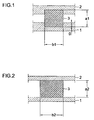
- a conventional transmission line for a millimeter wave or a micrometer wave has two parallely opposing conductive plates 1, 2 and a dielectric strip 3 disposed between the conductive plates.
- a normal type non radiative dielectric waveguide (“normal NRD”) is a kind of transmission line.
- the distance a2 between the conductive plates is adjusted to be equal to or less than a half wavelength of a wavelength of an electromagnetic wave so that the electromagnetic wave propagates only in the strip line 3.
- an excellent characteristics may be obtained without requiring a high dimensional accuracy since using the normal NRD guides as two NRD guides placed with a predetermined space the electric field energy distribution spreads wider than the case of using the hyper NRD guide.
- a configuration of the circular part in the component 102 shown in Fig. 4 is almost the same as the isolator in the component 101, and is constituted of a dielectric strip 40 that is continuous from the coupler part, a dielectric strip 45 that is continuous from the mixer part, another dielectric strip 44, a ferrite resonator 43 and a magnet as being not shown.
- Fig. 11A to 11C are views showing the configurations of one of the dielectric lines and the primary radiator of the rotational unit
- Fig. 11A is a top view
- Fig. 11B is a cross-sectional view.
- 61 indicates a dielectric resonator of the HE111 mode in a cylindrical shape, and is provided at a place where it is apart from the end part of the dielectric strip 60 with a predetermined distance.
- a window unit that is opened in a conical shape is provided in one part of the conductor plate 5, so that a radiation and an incidence of the electromagnetic waves are to be made from the upper part in the figure of this dielectric resonator 61.
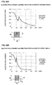
- a propagation of its LSE01 mode can be prevented without using the LSE01 mode suppresser in the multipointed circulator, and as a result a reduction of the number of parts can be made, thereby no translation loss is generated by the mode transformation of the LSM01 mode and the LSE01 mode.
- the coupling with its LSE01 mode can be prevented, without using the LSE01 mode suppresser in the mixer, the number of parts can be reduced.
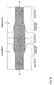
- the non radiative dielectric line part of the present invention by drawing the first type of non radiative dielectric lines closer, a coupler that couples them each other is formed. As a result, the non radiative dielectric lines can be strongly coupled in a short distance, thereby the coupler can be miniaturized.
Landscapes
- Waveguides (AREA)
- Waveguide Connection Structure (AREA)
- Waveguide Switches, Polarizers, And Phase Shifters (AREA)
Applications Claiming Priority (2)
| Application Number | Priority Date | Filing Date | Title |
|---|---|---|---|
| JP35737397 | 1997-12-25 | ||
| JP35737397A JP3303757B2 (ja) | 1997-12-25 | 1997-12-25 | 非放射性誘電体線路部品およびその集積回路 |
Publications (2)
| Publication Number | Publication Date |
|---|---|
| EP0926760A1 true EP0926760A1 (fr) | 1999-06-30 |
| EP0926760B1 EP0926760B1 (fr) | 2003-10-01 |
Family
ID=18453805
Family Applications (1)
| Application Number | Title | Priority Date | Filing Date |
|---|---|---|---|
| EP98124041A Expired - Lifetime EP0926760B1 (fr) | 1997-12-25 | 1998-12-17 | Composant électronique à guide d'ondes non-radiative et circuit intégré l'utilisant |
Country Status (7)
| Country | Link |
|---|---|
| US (1) | US6144267A (fr) |
| EP (1) | EP0926760B1 (fr) |
| JP (1) | JP3303757B2 (fr) |
| KR (1) | KR100291767B1 (fr) |
| CN (1) | CN1222076C (fr) |
| CA (1) | CA2256279C (fr) |
| DE (1) | DE69818625T2 (fr) |
Cited By (2)
| Publication number | Priority date | Publication date | Assignee | Title |
|---|---|---|---|---|
| WO2002067362A1 (fr) * | 2001-02-20 | 2002-08-29 | Nrdtech Co., Ltd. | Emetteur-recepteur a modulation par deplacement d'amplitude |
| EP1324422A3 (fr) * | 2001-12-18 | 2003-08-27 | Murata Manufacturing Co., Ltd. | Structure de couplage de ligne,mélangeur et dispositif de réception/transmission |
Families Citing this family (14)
| Publication number | Priority date | Publication date | Assignee | Title |
|---|---|---|---|---|
| JP3485054B2 (ja) * | 1999-12-28 | 2004-01-13 | 株式会社村田製作所 | 異種非放射性誘電体線路変換部構造およびその装置 |
| JP3735510B2 (ja) * | 2000-04-18 | 2006-01-18 | 株式会社村田製作所 | 伝送線路接続構造、高周波モジュールおよび通信装置 |
| AU2000261885A1 (en) * | 2000-08-02 | 2002-02-13 | Sensing Tech. Corp. | The multi-space structure amplifier |
| JP2002232212A (ja) * | 2001-01-31 | 2002-08-16 | Kyocera Corp | 非放射性誘電体線路用のパルス変調器およびそれを用いたミリ波送受信器 |
| KR100572114B1 (ko) * | 2002-06-15 | 2006-04-18 | 엔알디테크 주식회사 | Nrd 가이드를 이용한 밀리미터파 대역용 송수신기 |
| JP4095470B2 (ja) | 2003-02-26 | 2008-06-04 | 株式会社インテリジェント・コスモス研究機構 | Nrdガイドベンド |
| US20050143017A1 (en) * | 2003-12-31 | 2005-06-30 | Lopp Carl G. | Docking station for enabling landline telephones to send/receive calls via a docked walkie-talkie-type mobile telephone |
| DE102004031355A1 (de) * | 2004-03-31 | 2005-10-27 | Schleifring Und Apparatebau Gmbh | Drehübertrager mit dielektrischem Wellenleiter |
| US7109823B1 (en) | 2005-01-07 | 2006-09-19 | Hrl Lab Llc | Image guide coupler switch |
| KR101136519B1 (ko) * | 2010-03-09 | 2012-04-17 | (주)파트론 | 일체형 커플러-써큘레이터 및 그를 포함하는 전력 증폭기 |
| CN104064852A (zh) * | 2013-03-19 | 2014-09-24 | 德克萨斯仪器股份有限公司 | 用于将电磁信号从微带线发射到介电波导的喇叭天线 |
| US9270000B2 (en) * | 2013-03-21 | 2016-02-23 | Honeywell International Inc. | Waveguide circulator with improved transition to other transmission line media |
| JP2017011561A (ja) * | 2015-06-24 | 2017-01-12 | 京セラ株式会社 | 導波管構造体およびその製造方法 |
| IL292207B2 (en) * | 2019-10-17 | 2026-03-01 | Thruvision Ltd | High frequency heterodyne mixer |
Citations (1)
| Publication number | Priority date | Publication date | Assignee | Title |
|---|---|---|---|---|
| EP0767507A1 (fr) * | 1995-10-04 | 1997-04-09 | Murata Manufacturing Co., Ltd. | Guide d'onde diélectrique |
Family Cites Families (4)
| Publication number | Priority date | Publication date | Assignee | Title |
|---|---|---|---|---|
| JP3123293B2 (ja) * | 1993-03-05 | 2001-01-09 | 株式会社村田製作所 | 非放射性誘電体線路およびその製造方法 |
| JP2846278B2 (ja) * | 1996-02-19 | 1999-01-13 | 和歌山県 | 硬化不飽和ポリエステル樹脂廃棄物の再利用法 |
| JP3106972B2 (ja) * | 1996-08-29 | 2000-11-06 | 株式会社村田製作所 | 誘電体線路におけるダイオードマウント構造、検波器およびミキサ |
| JP3119176B2 (ja) * | 1996-10-23 | 2000-12-18 | 株式会社村田製作所 | 誘電体線路用アンテナ共用分配器および送受信装置 |
-
1997
- 1997-12-25 JP JP35737397A patent/JP3303757B2/ja not_active Expired - Fee Related
-
1998
- 1998-12-17 EP EP98124041A patent/EP0926760B1/fr not_active Expired - Lifetime
- 1998-12-17 CA CA002256279A patent/CA2256279C/fr not_active Expired - Fee Related
- 1998-12-17 DE DE69818625T patent/DE69818625T2/de not_active Expired - Lifetime
- 1998-12-18 US US09/216,109 patent/US6144267A/en not_active Expired - Lifetime
- 1998-12-24 KR KR1019980058186A patent/KR100291767B1/ko not_active Expired - Fee Related
- 1998-12-25 CN CNB981262252A patent/CN1222076C/zh not_active Expired - Fee Related
Patent Citations (1)
| Publication number | Priority date | Publication date | Assignee | Title |
|---|---|---|---|---|
| EP0767507A1 (fr) * | 1995-10-04 | 1997-04-09 | Murata Manufacturing Co., Ltd. | Guide d'onde diélectrique |
Non-Patent Citations (2)
| Title |
|---|
| TSUKASA YONEYAMA: "MILLIMETER-WAVE INTEGRATED CIRCUITS USING NONRADIATIVE DIELECTRIC WAVEGUIDE", ELECTRONICS & COMMUNICATIONS IN JAPAN, PART II - ELECTRONICS, vol. 74, no. 2, 1 February 1991 (1991-02-01), pages 20 - 28, XP000240840 * |
| XIAO L -L ET AL: "ANALYSIS OF GROOVE NRD WAVEGUIDE BEND USING THE COUPLED-MODE THEORY", INTERNATIONAL JOURNAL OF INFRARED AND MILLIMETER WAVES, vol. 13, no. 7, July 1992 (1992-07-01), pages 971 - 980, XP002022046 * |
Cited By (3)
| Publication number | Priority date | Publication date | Assignee | Title |
|---|---|---|---|---|
| WO2002067362A1 (fr) * | 2001-02-20 | 2002-08-29 | Nrdtech Co., Ltd. | Emetteur-recepteur a modulation par deplacement d'amplitude |
| EP1324422A3 (fr) * | 2001-12-18 | 2003-08-27 | Murata Manufacturing Co., Ltd. | Structure de couplage de ligne,mélangeur et dispositif de réception/transmission |
| US6931246B2 (en) | 2001-12-18 | 2005-08-16 | Murata Manufacturing Co., Ltd. | Line coupling structure, mixer, and receiving/transmitting apparatus comprised of suspended line and dielectric waveguide |
Also Published As
| Publication number | Publication date |
|---|---|
| JP3303757B2 (ja) | 2002-07-22 |
| DE69818625D1 (de) | 2003-11-06 |
| CA2256279C (fr) | 2002-09-24 |
| KR100291767B1 (ko) | 2001-06-01 |
| JPH11191706A (ja) | 1999-07-13 |
| US6144267A (en) | 2000-11-07 |
| CN1222076C (zh) | 2005-10-05 |
| DE69818625T2 (de) | 2004-08-19 |
| CA2256279A1 (fr) | 1999-06-25 |
| KR19990063422A (ko) | 1999-07-26 |
| CN1221230A (zh) | 1999-06-30 |
| EP0926760B1 (fr) | 2003-10-01 |
Similar Documents
| Publication | Publication Date | Title |
|---|---|---|
| EP0926760B1 (fr) | Composant électronique à guide d'ondes non-radiative et circuit intégré l'utilisant | |
| EP1473796B1 (fr) | Guide d'ondes diélectrique | |
| US7142165B2 (en) | Waveguide and slotted antenna array with moveable rows of spaced posts | |
| EP1398848B1 (fr) | Antenne à ouverture stratifiée et panneau à circuit multicouche comprenant la dite antenne | |
| EP0871239B1 (fr) | Dispositif d'antenne et module de radar | |
| US5943005A (en) | Multilayer dielectric line circuit | |
| EP1450433B1 (fr) | Circuit de suppression de modes parasites dans les lignes de transmission planaires | |
| KR100326958B1 (ko) | 이종의비방사성유전체도파관들간의선로변환부를갖는비방사성유전체도파관 | |
| JP3013798B2 (ja) | 交差線路 | |
| EP1324422B1 (fr) | Structure de couplage de ligne,mélangeur et dispositif de réception/transmission | |
| EP0869573B1 (fr) | Filtre diélectrique et appareil de communication l'utilisant | |
| US6342863B2 (en) | Antenna apparatus and antenna and tranceiver using the same | |
| JP3617397B2 (ja) | 誘電体線路導波管変換器、誘電体線路接続構造、1次放射器、発振器および送信装置 |
Legal Events
| Date | Code | Title | Description |
|---|---|---|---|
| PUAI | Public reference made under article 153(3) epc to a published international application that has entered the european phase |
Free format text: ORIGINAL CODE: 0009012 |
|
| 17P | Request for examination filed |
Effective date: 19981217 |
|
| AK | Designated contracting states |
Kind code of ref document: A1 Designated state(s): DE FI FR GB IT SE |
|
| AX | Request for extension of the european patent |
Free format text: AL;LT;LV;MK;RO;SI |
|
| AKX | Designation fees paid |
Free format text: DE FI FR GB IT SE |
|
| GRAH | Despatch of communication of intention to grant a patent |
Free format text: ORIGINAL CODE: EPIDOS IGRA |
|
| GRAS | Grant fee paid |
Free format text: ORIGINAL CODE: EPIDOSNIGR3 |
|
| GRAA | (expected) grant |
Free format text: ORIGINAL CODE: 0009210 |
|
| AK | Designated contracting states |
Kind code of ref document: B1 Designated state(s): DE FI FR GB IT SE |
|
| PG25 | Lapsed in a contracting state [announced via postgrant information from national office to epo] |
Ref country code: IT Free format text: LAPSE BECAUSE OF FAILURE TO SUBMIT A TRANSLATION OF THE DESCRIPTION OR TO PAY THE FEE WITHIN THE PRESCRIBED TIME-LIMIT;WARNING: LAPSES OF ITALIAN PATENTS WITH EFFECTIVE DATE BEFORE 2007 MAY HAVE OCCURRED AT ANY TIME BEFORE 2007. THE CORRECT EFFECTIVE DATE MAY BE DIFFERENT FROM THE ONE RECORDED. Effective date: 20031001 Ref country code: FI Free format text: LAPSE BECAUSE OF FAILURE TO SUBMIT A TRANSLATION OF THE DESCRIPTION OR TO PAY THE FEE WITHIN THE PRESCRIBED TIME-LIMIT Effective date: 20031001 |
|
| REG | Reference to a national code |
Ref country code: GB Ref legal event code: FG4D |
|
| REF | Corresponds to: |
Ref document number: 69818625 Country of ref document: DE Date of ref document: 20031106 Kind code of ref document: P |
|
| PG25 | Lapsed in a contracting state [announced via postgrant information from national office to epo] |
Ref country code: SE Free format text: LAPSE BECAUSE OF FAILURE TO SUBMIT A TRANSLATION OF THE DESCRIPTION OR TO PAY THE FEE WITHIN THE PRESCRIBED TIME-LIMIT Effective date: 20040101 |
|
| ET | Fr: translation filed | ||
| PLBE | No opposition filed within time limit |
Free format text: ORIGINAL CODE: 0009261 |
|
| STAA | Information on the status of an ep patent application or granted ep patent |
Free format text: STATUS: NO OPPOSITION FILED WITHIN TIME LIMIT |
|
| 26N | No opposition filed |
Effective date: 20040702 |
|
| PGFP | Annual fee paid to national office [announced via postgrant information from national office to epo] |
Ref country code: DE Payment date: 20121213 Year of fee payment: 15 |
|
| PGFP | Annual fee paid to national office [announced via postgrant information from national office to epo] |
Ref country code: GB Payment date: 20121212 Year of fee payment: 15 |
|
| PGFP | Annual fee paid to national office [announced via postgrant information from national office to epo] |
Ref country code: FR Payment date: 20130107 Year of fee payment: 15 |
|
| REG | Reference to a national code |
Ref country code: DE Ref legal event code: R119 Ref document number: 69818625 Country of ref document: DE |
|
| GBPC | Gb: european patent ceased through non-payment of renewal fee |
Effective date: 20131217 |
|
| REG | Reference to a national code |
Ref country code: FR Ref legal event code: ST Effective date: 20140829 |
|
| REG | Reference to a national code |
Ref country code: DE Ref legal event code: R119 Ref document number: 69818625 Country of ref document: DE Effective date: 20140701 |
|
| PG25 | Lapsed in a contracting state [announced via postgrant information from national office to epo] |
Ref country code: DE Free format text: LAPSE BECAUSE OF NON-PAYMENT OF DUE FEES Effective date: 20140701 |
|
| PG25 | Lapsed in a contracting state [announced via postgrant information from national office to epo] |
Ref country code: FR Free format text: LAPSE BECAUSE OF NON-PAYMENT OF DUE FEES Effective date: 20131231 Ref country code: GB Free format text: LAPSE BECAUSE OF NON-PAYMENT OF DUE FEES Effective date: 20131217 |