EP0926810A1 - Perfectionnement aux régulateurs d'alternateur polyphase de véhicule - Google Patents
Perfectionnement aux régulateurs d'alternateur polyphase de véhicule Download PDFInfo
- Publication number
- EP0926810A1 EP0926810A1 EP98403260A EP98403260A EP0926810A1 EP 0926810 A1 EP0926810 A1 EP 0926810A1 EP 98403260 A EP98403260 A EP 98403260A EP 98403260 A EP98403260 A EP 98403260A EP 0926810 A1 EP0926810 A1 EP 0926810A1
- Authority
- EP
- European Patent Office
- Prior art keywords
- detection
- current
- potential
- regulator according
- transistors
- Prior art date
- Legal status (The legal status is an assumption and is not a legal conclusion. Google has not performed a legal analysis and makes no representation as to the accuracy of the status listed.)
- Granted
Links
- 238000001514 detection method Methods 0.000 claims description 43
- 230000000712 assembly Effects 0.000 claims description 4
- 238000000429 assembly Methods 0.000 claims description 4
- 230000001747 exhibiting effect Effects 0.000 claims 1
- 230000007423 decrease Effects 0.000 description 4
- 230000035945 sensitivity Effects 0.000 description 4
- 238000004804 winding Methods 0.000 description 3
- 230000033228 biological regulation Effects 0.000 description 2
- 238000010586 diagram Methods 0.000 description 2
- 230000005284 excitation Effects 0.000 description 2
- 239000006185 dispersion Substances 0.000 description 1
- 235000021183 entrée Nutrition 0.000 description 1
- 238000004519 manufacturing process Methods 0.000 description 1
- 238000005259 measurement Methods 0.000 description 1
- 238000000034 method Methods 0.000 description 1
- 239000003607 modifier Substances 0.000 description 1
- 230000000750 progressive effect Effects 0.000 description 1
- 230000001052 transient effect Effects 0.000 description 1
Images


Classifications
-
- G—PHYSICS
- G01—MEASURING; TESTING
- G01R—MEASURING ELECTRIC VARIABLES; MEASURING MAGNETIC VARIABLES
- G01R19/00—Arrangements for measuring currents or voltages or for indicating presence or sign thereof
- G01R19/0038—Circuits for comparing several input signals and for indicating the result of this comparison, e.g. equal, different, greater, smaller (comparing pulses or pulse trains according to amplitude)
-
- H—ELECTRICITY
- H02—GENERATION; CONVERSION OR DISTRIBUTION OF ELECTRIC POWER
- H02P—CONTROL OR REGULATION OF ELECTRIC MOTORS, ELECTRIC GENERATORS OR DYNAMO-ELECTRIC CONVERTERS; CONTROLLING TRANSFORMERS, REACTORS OR CHOKE COILS
- H02P9/00—Arrangements for controlling electric generators for the purpose of obtaining a desired output
- H02P9/14—Arrangements for controlling electric generators for the purpose of obtaining a desired output by variation of field
- H02P9/26—Arrangements for controlling electric generators for the purpose of obtaining a desired output by variation of field using discharge tubes or semiconductor devices
- H02P9/30—Arrangements for controlling electric generators for the purpose of obtaining a desired output by variation of field using discharge tubes or semiconductor devices using semiconductor devices
- H02P9/305—Arrangements for controlling electric generators for the purpose of obtaining a desired output by variation of field using discharge tubes or semiconductor devices using semiconductor devices controlling voltage
Definitions
- the present invention relates to regulators motor vehicle alternator.
- FIG. 1 a conventional three-phase alternator circuit.
- This circuit includes three armature windings alternator EN1, EN2, EN3 mounted in star, one bridge rectifier P consisting of three pairs of diodes and one regulator R having two phase inputs ⁇ 1 and ⁇ 2 receiving two of the three phase potentials of armature windings EN1, EN2, EN3.
- this regulator R comprises a circuit DP to detect the appearance of a voltage between the two phase terminals ⁇ 1 and ⁇ 2 during rotation of the alternator and trigger the regulation of the battery voltage when this rotation is thus detected.
- a DP circuit ensures the alternator self-priming.
- the inventors propose, in a patent application filed on the same day as this request to integrate means to a regulator to detect this particular level of potential on at least a phase terminal and to initiate operation of the regulator in an accelerated mode when this level of potential is detected.
- the current source transistors block when negative potentials are applied to both mounting inputs.
- An object of the invention is therefore to propose a detection assembly which on the one hand is of great sensitivity (200 mV or less: 50mV) and who else part is able to function independently of the level of potential on the phase inputs and in particular with potential levels on the phase inputs strongly negative (around 10 Volts below mass, for example).
- the invention proposes a regulator of a polyphase alternator of a motor vehicle comprising means for detecting a voltage between terminals of phase intended to receive phase potentials of said alternator, characterized in that said means of detection include at least one transistor assembly forming a current mirror whose two branches are at one end respectively connected to one and the other of the two phase terminals and are supplied to their other end by transistors forming current sources which deliver in the said branches currents of the same intensity, the two branches also having resistors of different values, so that one of transistors of the assemblies forming current sources limit on a predetermined current value when a potential difference greater than a given threshold appears between the two phase terminals, this limitation causing the level change of a logic output controlled by the potential at a point of said branch between the transistor forming the current source and the transistor of the assembly forming current mirror.
- FIG. 1 An example of a DP detection circuit conforming to an embodiment of the invention and capable of operate with strongly peak values negative (- 10 volts compared to ground potential) is illustrated in figure 2.
- This circuit includes two mounted current mirrors between terminals ⁇ 1 and ⁇ 2 and formed one by two NPN transistors T1, T9, the other by two NPN transistors T2, T10.
- terminal ⁇ 1 is connected via a resistor R10 at the emitter (point E1) of the transistor T1 and by a resistor R21 at the emitter of the transistor T10.
- Terminal ⁇ 2 is connected by a resistor R11 to the emitter of transistor T2 and by a resistor R20 to the emitter of transistor T9.
- the basics of T2 transistors and T10 are interconnected. The same is true of bases of transistors T1 and T9.
- Resistors R10 and R11 are worth higher than that of resistors R20 and R21.
- Diodes D1 and D2 are mounted between the transmitter and the base of transistors T1 and T2 to protect said transistors transistors against reverse polarity of junctions transmitter-base.
- the collectors of transistors T1, T10, T9 and T2 are connected to PNP transistor collectors T7, T5, T6 and T8 whose bases are interconnected and whose transmitters are connected to a power line under a voltage UB + itself connected to the pale positive of the vehicle battery.
- the circuit has two terminals of logic output S1 and S2.
- Terminal S1 is connected to the collector of a PNP transistor T3, the base of which is connected to collectors of transistors T1 and T7.
- the transmitter of this transistor T3 is connected to line UB +.
- the terminal of logic output S1 is also connected to ground by through a resistor R9.
- the terminal S2 is connected to the collector of a PNP transistor T4, the base of which is connected to the collectors of the transistors T2 and T8 while its transmitter is connected to the line UB +.
- the logic output terminal S2 is itself connected to the mass via a resistor R12.
- resistors R9 and R12 do not part of the detector itself: they serve as load resistors of the detector output stages constituted by the transistors T3 and T4.
- the detection circuit shown on FIG. 2 comprises a current generator G.
- This generator G includes a high value resistor R5 rise between line UB + and the base of a transistor T11 NPN. Said base of transistor T11 is connected to ground via two diodes D3 and D4 of thermal compensation in series with a Zener diode DZ1.
- the emitter of transistor T11 is connected to ground by through a resistor R3, as well as by through a sub-circuit which includes in series a resistor R4 and a MOSFET type transistor M1, whose command will be explained later so detailed.
- the collector and the base of transistor T11 are connected respectively to the collectors of the transistors T13 and PN12 type T12 mounted in current mirror.
- the basics transistors T13 and T12 are connected to the bases of the transistors T5 to T8, while their transmitters are connected to the UB + line.
- this embodiment incorporates elements of the detector described in FR-2,678,070.
- Resistors R7 and R8 y are replaced by the working transistors T7 and T8 in current source.
- the detector represented in FIG. 2 does not have a ground potential and the phase inputs ⁇ 1 and ⁇ 2 can have all the values lower than the potential U B + without affecting the level of detection (200 mV or less).
- Resistor R6 serves to polarize the armature of the alternator when it is stopped.
- the value of this resistance R6 is strong enough not to prevent the application of the strongly negative potential on the phase inputs ⁇ 1 and ⁇ 2 (- 10 volts compared to the mass).
- the DP detector works as follows: transistor T11 delivers a current (20 ⁇ A) calibrated by resistance R3 and diodes D3, D4 and DZ1.
- the diodes D3 and D4 thermally compensate the emitter-base junction of T11 and the zener voltage of DZ1.
- the current delivered by the transistor T11 is copied in a ratio 1 (20 ⁇ A) by the T12 transistors and T5 to T8.
- T5 and T6 (20 ⁇ A) cross transistors T9 and T10.
- the resistors R10 and R11 being of a higher than that of resistors R20 and R21, the currents copied by T1 and T2 are lower than currents in T9 and T10.
- the alternator is the order of 12 ⁇ A while the current in T9 and in T10 is 20 ⁇ A.
- Figure 3 shows the voltage variation on outputs S1 and S2 when the potential of ⁇ 2 varies sinusoidally with respect to ⁇ 1. This corresponds at f.e.m. produced by the remanence of the circuit magnetic of the inductor when the alternator enters rotation.
- the level of detection of a difference of potentials between terminals ⁇ 2 and ⁇ 1 is preferably 200 mV or less. This level of 200 mV detection between phases allows self-priming of the alternator at low speed ( ⁇ 1000 rpm) without initial excitation current.
- T1 and T9 are linked, the potentials transmitters of T1 and T9 are identical at the time of detection, because at this moment, the currents are identical (20 ⁇ A) in T1 and T9; T2 and T10 (there is one residual offset of 2 to 3 mV: offset voltage).
- the level of detection is proportional to the difference in resistance values R10 - R20 (when the potential of ⁇ 1 decreases compared to at the potential of ⁇ 2) and that the detection level is proportional to the difference in resistance values R11 - R21 (when the potential ⁇ 2 decreases compared to the potential of ⁇ 1).
- FIG. 4 represents a simplified variant of phase signal detector when you don't want to detect only one alternation.
- the detector has only one current mirror (T1, T9) and a single logic output (S1, controlled by the transistor T3). With this embodiment, we do not detects a potential difference only when ⁇ 1 ⁇ 2.
- This level of detection of a difference in potential between phases of the order of 50 mV to 200 mV allows self-priming of the alternator at low speed rotation ( ⁇ 1000 rpm) without excitation current initial.
- the solution is to increase the level of detection when the f.e.m. between ⁇ 1 and ⁇ 2 is high, while remaining below any possibility of charging : for example, changing the detection level may go from 50 or 200 mV to 800 mV when the f.e.m. Between phases exceeds 7 volts. This measurement of f.e.m. may be realized by the phase signal regulation circuit already used in a lot of regulators says "multifunction".
- the current generator G enables this change in detection level.
- the regulator detects higher signal amplitude between phases at 7 volts, it turns on transistor M1, so that resistance R4 is put in parallel on R3.
- the increase in current in T11, T5, T6, T7, T8 increases the level of detection sought: we obtain a detection level of 800 mV for currents of 100 ⁇ A in T11, T7, T5, T6 and T8.
Landscapes
- Physics & Mathematics (AREA)
- General Physics & Mathematics (AREA)
- Engineering & Computer Science (AREA)
- Power Engineering (AREA)
- Control Of Eletrric Generators (AREA)
Abstract
Description
- il comporte deux sorties logiques et en ce que lesdits montages de transistors formant miroir et sources de courant sont dédoublés pour entraíner le changement de niveau de l'une ou l'autre desdites sorties logiques selon le sens de la différence de potentiel entre les bornes de phase.
- le niveau de détection que permettent lesdits moyens est de 200 mV ou inférieur.
- la résistance sur la branche du montage formant miroir de courant dont un potentiel commande la sortie logique est égale à 20 KΩ, la résistance sur l'autre branche étant égale à 10 KΩ.
- la résistance sur la branche du montage formant miroir de courant dont un potentiel commande la sortie logique est égale à 10 KΩ le niveau de détection que permettent les moyens de détection est de l'ordre de 50 mV.
- la résistance sur la branche du montage formant miroir de courant dont un potentiel commande la sortie logique est égale à 5 KΩ, la résistance sur l'autre branche étant égale à 2,5 KΩ.
- la résistance sur la branche du montage formant miroir de courant dont un potentiel commande la sortie logique est égale à 2,5 KΩ le régulateur comporte des moyens pour modifier le niveau de détection de la tension entre les bornes de phase lorsque le potentiel reçu sur lesdites bornes est supérieur à une valeur donnée.
- La figure 1 est une représentation schématique d'un circuit d'alternateur triphasé conventionnel.
- La figure 2 est un schéma d'un montage possible pour les moyens de détection de la tension entre des bornes de phase d'un régulateur conforme à un mode de réalisation possible de l'invention.
- La figure 3 est illustre un exemple de signaux en entrée et en sortie du montage de la figure 2 lorsque l'alternateur entre en rotation.
- La figure 4 est un schéma d'un autre montage possible pour l'invention.
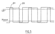
- La figure 5 est un graphe sur lequel on a porté les signaux de phase en sortie des enroulements d'induit de l'alternateur, lorsque le régulateur est sous charge.
pour un niveau de détection de 200mV, on a :
Claims (12)
- Régulateur d'alternateur polyphasé de véhicule automobile comportant des moyens pour détecter une tension entre des bornes de phase destinées à recevoir des potentiels de phase dudit alternateur, caractérisé en ce que lesdits moyens de détection comportent au moins un montage de transistors (T1, T9 ; T2, T10) formant miroir de courant dont les deux branches sont à une extrémité respectivement reliées à l'une et l'autre des deux bornes de phase et sont alimentées à leur autre extrémité par des transistors (T6, T7 ; T5, T8) formant sources de courant qui délivrent dans lesdites branches des courants de même intensité, les deux branches présentant en outre des résistances de valeurs différentes R10, R20 ; R11, R21, de sorte que l'un (T7, T8) des transistors des montages formant sources de courant se limite sur une valeur de courant prédéterminée (20µA) lorsqu'une différence de potentiel supérieure à un seuil donné apparaít entre les deux bornes de phase, cette limitation entraínant le changement de niveau d'une sortie logique (S1, S2) commandée par le potentiel en un point de ladite branche entre le transistor (T7, T8) formant source de courant et le transistor (T1, T2) du montage formant miroir de courant.
- Régulateur selon la revendication 1, caractérisé en ce qu'il comporte deux sorties logiques et en ce que lesdits montages (T1, T9 ; T2, T10 ; T6, T7 ; T5, T8) de transistors formant miroir et sources de courant sont dédoublés pour entraíner le changement de niveau de l'une ou l'autre desdites sorties logiques selon le sens de la différence de potentiel entre les bornes de phase.
- Régulateur selon la revendication 1 ou 2, caractérisé en ce que le niveau de détection de la tension entre phases est lié à la différence de valeurs des résistances (R10 - R20 d'une part, R11 - R21 d'autre part) des moyens de détection).
- Régulateur selon l'une des revendications précédentes, caractérisé en ce que le niveau de détection de la tension entre phases est proportionnel à la différence de valeur des résistances (R10 - R20 d'une part, R11 - R21 d'autre part) des moyens de détection).
- Régulateur selon la revendication 1, caractérisé en ce que les moyens de détection ne comportent qu'un seul miroir de courant (T1, T9) et une seule sortie logique (S1, commandé par le transistor T3) pour ne détecter la f.e.m. entre 1 et 2 que dans un seul sens.
- Régulateur selon l'une des revendications 1 à 5, caractérisé en ce que le niveau de détection que permettent lesdits moyens est de 200 mV ou inférieur.
- Régulateur selon la revendication 6, caractérisé en ce que la résistance sur la branche du montage formant miroir de courant dont un potentiel commande la sortie logique est égale à 20 KΩ, la résistance sur l'autre branche étant égale à 10 KΩ.
- Régulateur selon la revendication 6, caractérisé en ce que la résistance sur la branche du montage formant miroir de courant dont un potentiel commande la sortie logique est égale à 10 KΩ
- Régulateur selon l'une des revendications 1 à 5, caractérisé en ce que le niveau de détection que permettent les moyens de détection est de l'ordre de 50 mV.
- Régulateur selon la revendication 9, caractérisé en ce que la résistance sur la branche du montage formant miroir de courant dont un potentiel commande la sortie logique est égale à 5 KΩ, la résistance sur l'autre branche étant égale à 2,5 KΩ.
- Régulateur selon la revendication 9, caractérisé en ce que la résistance sur la branche du montage formant miroir de courant dont un potentiel commande la sortie logique est égale à 2,5 KΩ.
- Régulateur selon une des revendications précédentes, caractérisé en ce qu'il comporte des moyens (M1, R4) pour modifier le niveau de détection de la tension entre les bornes de phase lorsque le potentiel reçu sur lesdites bornes est supérieur à une valeur donnée.
Applications Claiming Priority (2)
| Application Number | Priority Date | Filing Date | Title |
|---|---|---|---|
| FR9716496 | 1997-12-24 | ||
| FR9716496A FR2773018B1 (fr) | 1997-12-24 | 1997-12-24 | Perfectionnements aux regulateurs d'alternateur polyphase de vehicule automobile |
Publications (2)
| Publication Number | Publication Date |
|---|---|
| EP0926810A1 true EP0926810A1 (fr) | 1999-06-30 |
| EP0926810B1 EP0926810B1 (fr) | 2008-07-30 |
Family
ID=9515125
Family Applications (1)
| Application Number | Title | Priority Date | Filing Date |
|---|---|---|---|
| EP98403260A Expired - Lifetime EP0926810B1 (fr) | 1997-12-24 | 1998-12-22 | Perfectionnement aux régulateurs d'alternateur polyphasés de véhicule |
Country Status (6)
| Country | Link |
|---|---|
| US (1) | US6034512A (fr) |
| EP (1) | EP0926810B1 (fr) |
| BR (1) | BR9805546B1 (fr) |
| DE (1) | DE69839796D1 (fr) |
| ES (1) | ES2311296T3 (fr) |
| FR (1) | FR2773018B1 (fr) |
Families Citing this family (3)
| Publication number | Priority date | Publication date | Assignee | Title |
|---|---|---|---|---|
| FR2821699B1 (fr) * | 2001-03-02 | 2003-05-30 | Valeo Equip Electr Moteur | Alternateur de vehicule automobile a sortie d'information d'excitation |
| US20030117018A1 (en) * | 2001-12-21 | 2003-06-26 | Young James M. | Current mirror seatbelt interface circuit |
| US8188693B2 (en) * | 2009-11-04 | 2012-05-29 | Rockwell Automation Technologies, Inc. | DC bus boost method and system for regenerative brake |
Citations (3)
| Publication number | Priority date | Publication date | Assignee | Title |
|---|---|---|---|---|
| FR2343255A1 (fr) * | 1976-02-17 | 1977-09-30 | Western Electric Co | Comparateur de tension a fenetre |
| FR2678070A1 (fr) * | 1991-06-18 | 1992-12-24 | Valeo Equip Electr Moteur | Circuit de detection de la tension entre phases d'un alternateur pour la mise en service d'un regulateur associe a un tel alternateur. |
| FR2730359A1 (fr) * | 1995-02-07 | 1996-08-09 | Valeo Equip Electr Moteur | Dispositif regulateur de la tension de charge d'une batterie par un alternateur a moyens d'amorcage perfectionnes, notamment pour vehicule automobile |
Family Cites Families (3)
| Publication number | Priority date | Publication date | Assignee | Title |
|---|---|---|---|---|
| FR2679718B1 (fr) * | 1991-07-25 | 1993-12-24 | Valeo Equipements Elect Moteur | Circuit regulateur de la tension de charge d'une batterie par un alternateur. |
| JP3226689B2 (ja) * | 1993-12-24 | 2001-11-05 | 株式会社日立製作所 | 自己診断機能を備えた充電発電機 |
| US5701089A (en) * | 1995-10-12 | 1997-12-23 | Autozone, Inc. | Alternator/starter testing device |
-
1997
- 1997-12-24 FR FR9716496A patent/FR2773018B1/fr not_active Expired - Fee Related
-
1998
- 1998-12-22 ES ES98403260T patent/ES2311296T3/es not_active Expired - Lifetime
- 1998-12-22 EP EP98403260A patent/EP0926810B1/fr not_active Expired - Lifetime
- 1998-12-22 DE DE69839796T patent/DE69839796D1/de not_active Expired - Lifetime
- 1998-12-24 US US09/220,671 patent/US6034512A/en not_active Expired - Lifetime
- 1998-12-24 BR BRPI9805546-1A patent/BR9805546B1/pt not_active IP Right Cessation
Patent Citations (3)
| Publication number | Priority date | Publication date | Assignee | Title |
|---|---|---|---|---|
| FR2343255A1 (fr) * | 1976-02-17 | 1977-09-30 | Western Electric Co | Comparateur de tension a fenetre |
| FR2678070A1 (fr) * | 1991-06-18 | 1992-12-24 | Valeo Equip Electr Moteur | Circuit de detection de la tension entre phases d'un alternateur pour la mise en service d'un regulateur associe a un tel alternateur. |
| FR2730359A1 (fr) * | 1995-02-07 | 1996-08-09 | Valeo Equip Electr Moteur | Dispositif regulateur de la tension de charge d'une batterie par un alternateur a moyens d'amorcage perfectionnes, notamment pour vehicule automobile |
Also Published As
| Publication number | Publication date |
|---|---|
| DE69839796D1 (de) | 2008-09-11 |
| FR2773018A1 (fr) | 1999-06-25 |
| US6034512A (en) | 2000-03-07 |
| BR9805546A (pt) | 1999-12-21 |
| ES2311296T3 (es) | 2009-02-01 |
| FR2773018B1 (fr) | 2000-03-10 |
| EP0926810B1 (fr) | 2008-07-30 |
| BR9805546B1 (pt) | 2011-03-09 |
Similar Documents
| Publication | Publication Date | Title |
|---|---|---|
| EP0408436B1 (fr) | Circuit de détection du signal phase alternateur polyphase de contrôle d'un régulateur de charge de batterie de véhicule automobile et son utilisation | |
| EP0925641B1 (fr) | Dispositif de detection de la position angulaire pour le pilotage d'un moteur synchrone a excitation par aimant permanent | |
| FR2723904A1 (fr) | Unite d'entrainement electrique pour automobiles | |
| FR2524729A1 (fr) | Circuit d'excitation pour moteur a courant continu sans balais | |
| EP0926810A1 (fr) | Perfectionnement aux régulateurs d'alternateur polyphase de véhicule | |
| EP0120723B1 (fr) | Procédé et dispositif pour détecter si un moteur à courant continu est ralenti, et moteur comportant un tel dispositif | |
| EP0829796B1 (fr) | Contrôleur de tension à sensibilité aux variations de température atténuée | |
| WO2000049420A1 (fr) | Dispositif de mesure de courant et procede correspondant | |
| EP0926503B1 (fr) | Regulateur d'alternateur polyphasé de véhicule automobile | |
| EP3938792B1 (fr) | Installation electrique comportant un module de surveillance | |
| EP0726633B1 (fr) | Dispositif régulateur de la tension de charge d'une batterie par un alternateur à moyens d'amorçage perfectionnés, notamment pour véhicule automobile | |
| FR2806553A1 (fr) | Redresseur pour alternateur polyphase de vehicules automobiles a pertes energetiques reduites | |
| EP0159263A1 (fr) | Procédé et dispositif de contrôle de niveau de liquide dans un réservoir | |
| EP1364438A1 (fr) | Alternateur de vehicule automobile a sortie d'information d'excitation | |
| EP3938793B1 (fr) | Installation electrique comportant un module de surveillance | |
| FR2627916A1 (fr) | Dispositif de commande de moteur a courant continu | |
| EP0609113B1 (fr) | Dispositif de mesure d'un paramètre électrique continu, tel qu'une tension | |
| FR2678070A1 (fr) | Circuit de detection de la tension entre phases d'un alternateur pour la mise en service d'un regulateur associe a un tel alternateur. | |
| FR2596596A1 (fr) | Procede et dispositif de transmission d'informations entre deux circuits electroniques | |
| EP1414147B1 (fr) | Procédé de mesure de la puissance fournie par un moteur | |
| EP1199803B1 (fr) | Asservissement en amplitude d'un signal alternatif produit par un dispositif électronique, tel un circuit oscillateur | |
| WO2017121955A1 (fr) | Circuit d'excitation pour un resolveur | |
| FR2705455A1 (fr) | Capteur de déplacement relatif par mesure de réluctance magnétique, capteur de couple utilisant un tel capteur et application à un système de direction assistée de véhicule. | |
| EP0449723A1 (fr) | Dispositif de mise en forme d'un signal impulsionnel de capteur | |
| FR3100947A1 (fr) | Procédé de contrôle en vitesse de moteurs sans balai. |
Legal Events
| Date | Code | Title | Description |
|---|---|---|---|
| PUAI | Public reference made under article 153(3) epc to a published international application that has entered the european phase |
Free format text: ORIGINAL CODE: 0009012 |
|
| AK | Designated contracting states |
Kind code of ref document: A1 Designated state(s): DE ES GB IT |
|
| AX | Request for extension of the european patent |
Free format text: AL;LT;LV;MK;RO;SI |
|
| 17P | Request for examination filed |
Effective date: 19991223 |
|
| AKX | Designation fees paid |
Free format text: DE ES GB IT |
|
| GRAP | Despatch of communication of intention to grant a patent |
Free format text: ORIGINAL CODE: EPIDOSNIGR1 |
|
| GRAS | Grant fee paid |
Free format text: ORIGINAL CODE: EPIDOSNIGR3 |
|
| GRAA | (expected) grant |
Free format text: ORIGINAL CODE: 0009210 |
|
| AK | Designated contracting states |
Kind code of ref document: B1 Designated state(s): DE ES GB IT |
|
| REG | Reference to a national code |
Ref country code: GB Ref legal event code: FG4D Free format text: NOT ENGLISH |
|
| REF | Corresponds to: |
Ref document number: 69839796 Country of ref document: DE Date of ref document: 20080911 Kind code of ref document: P |
|
| REG | Reference to a national code |
Ref country code: ES Ref legal event code: FG2A Ref document number: 2311296 Country of ref document: ES Kind code of ref document: T3 |
|
| PLBE | No opposition filed within time limit |
Free format text: ORIGINAL CODE: 0009261 |
|
| STAA | Information on the status of an ep patent application or granted ep patent |
Free format text: STATUS: NO OPPOSITION FILED WITHIN TIME LIMIT |
|
| 26N | No opposition filed |
Effective date: 20090506 |
|
| PGFP | Annual fee paid to national office [announced via postgrant information from national office to epo] |
Ref country code: GB Payment date: 20141218 Year of fee payment: 17 Ref country code: ES Payment date: 20141224 Year of fee payment: 17 |
|
| PGFP | Annual fee paid to national office [announced via postgrant information from national office to epo] |
Ref country code: IT Payment date: 20141223 Year of fee payment: 17 Ref country code: DE Payment date: 20141211 Year of fee payment: 17 |
|
| REG | Reference to a national code |
Ref country code: DE Ref legal event code: R119 Ref document number: 69839796 Country of ref document: DE |
|
| GBPC | Gb: european patent ceased through non-payment of renewal fee |
Effective date: 20151222 |
|
| PG25 | Lapsed in a contracting state [announced via postgrant information from national office to epo] |
Ref country code: DE Free format text: LAPSE BECAUSE OF NON-PAYMENT OF DUE FEES Effective date: 20160701 Ref country code: GB Free format text: LAPSE BECAUSE OF NON-PAYMENT OF DUE FEES Effective date: 20151222 |
|
| PG25 | Lapsed in a contracting state [announced via postgrant information from national office to epo] |
Ref country code: IT Free format text: LAPSE BECAUSE OF NON-PAYMENT OF DUE FEES Effective date: 20151222 |
|
| REG | Reference to a national code |
Ref country code: ES Ref legal event code: FD2A Effective date: 20170126 |
|
| PG25 | Lapsed in a contracting state [announced via postgrant information from national office to epo] |
Ref country code: ES Free format text: LAPSE BECAUSE OF NON-PAYMENT OF DUE FEES Effective date: 20151223 |