EP0926833A1 - Circuit diviseur et étage à transistor pour celui-ci - Google Patents
Circuit diviseur et étage à transistor pour celui-ci Download PDFInfo
- Publication number
- EP0926833A1 EP0926833A1 EP98310190A EP98310190A EP0926833A1 EP 0926833 A1 EP0926833 A1 EP 0926833A1 EP 98310190 A EP98310190 A EP 98310190A EP 98310190 A EP98310190 A EP 98310190A EP 0926833 A1 EP0926833 A1 EP 0926833A1
- Authority
- EP
- European Patent Office
- Prior art keywords
- output
- signal
- dividing circuit
- input
- stage
- Prior art date
- Legal status (The legal status is an assumption and is not a legal conclusion. Google has not performed a legal analysis and makes no representation as to the accuracy of the status listed.)
- Withdrawn
Links
- 238000010586 diagram Methods 0.000 description 5
- XUIMIQQOPSSXEZ-UHFFFAOYSA-N Silicon Chemical compound [Si] XUIMIQQOPSSXEZ-UHFFFAOYSA-N 0.000 description 3
- 229910052710 silicon Inorganic materials 0.000 description 3
- 239000010703 silicon Substances 0.000 description 3
- 230000001419 dependent effect Effects 0.000 description 2
- 230000000694 effects Effects 0.000 description 2
- 230000000630 rising effect Effects 0.000 description 2
- 238000005516 engineering process Methods 0.000 description 1
Images




Classifications
-
- H—ELECTRICITY
- H03—ELECTRONIC CIRCUITRY
- H03L—AUTOMATIC CONTROL, STARTING, SYNCHRONISATION OR STABILISATION OF GENERATORS OF ELECTRONIC OSCILLATIONS OR PULSES
- H03L7/00—Automatic control of frequency or phase; Synchronisation
- H03L7/06—Automatic control of frequency or phase; Synchronisation using a reference signal applied to a frequency- or phase-locked loop
- H03L7/16—Indirect frequency synthesis, i.e. generating a desired one of a number of predetermined frequencies using a frequency- or phase-locked loop
- H03L7/18—Indirect frequency synthesis, i.e. generating a desired one of a number of predetermined frequencies using a frequency- or phase-locked loop using a frequency divider or counter in the loop
- H03L7/183—Indirect frequency synthesis, i.e. generating a desired one of a number of predetermined frequencies using a frequency- or phase-locked loop using a frequency divider or counter in the loop a time difference being used for locking the loop, the counter counting between fixed numbers or the frequency divider dividing by a fixed number
-
- H—ELECTRICITY
- H03—ELECTRONIC CIRCUITRY
- H03K—PULSE TECHNIQUE
- H03K23/00—Pulse counters comprising counting chains; Frequency dividers comprising counting chains
- H03K23/40—Gating or clocking signals applied to all stages, i.e. synchronous counters
- H03K23/42—Out-of-phase gating or clocking signals applied to counter stages
- H03K23/44—Out-of-phase gating or clocking signals applied to counter stages using field-effect transistors
-
- H—ELECTRICITY
- H03—ELECTRONIC CIRCUITRY
- H03K—PULSE TECHNIQUE
- H03K23/00—Pulse counters comprising counting chains; Frequency dividers comprising counting chains
- H03K23/40—Gating or clocking signals applied to all stages, i.e. synchronous counters
- H03K23/50—Gating or clocking signals applied to all stages, i.e. synchronous counters using bi-stable regenerative trigger circuits
- H03K23/54—Ring counters, i.e. feedback shift register counters
- H03K23/544—Ring counters, i.e. feedback shift register counters with a base which is an odd number
-
- H—ELECTRICITY
- H03—ELECTRONIC CIRCUITRY
- H03K—PULSE TECHNIQUE
- H03K23/00—Pulse counters comprising counting chains; Frequency dividers comprising counting chains
- H03K23/64—Pulse counters comprising counting chains; Frequency dividers comprising counting chains with a base or radix other than a power of two
- H03K23/66—Pulse counters comprising counting chains; Frequency dividers comprising counting chains with a base or radix other than a power of two with a variable counting base, e.g. by presetting or by adding or suppressing pulses
Definitions
- This invention relates to a divider circuit, particularly but not exclusively for dividing by odd integers, and to a transistor stage therefor.
- Clock divider circuits are useful in a number of applications, particularly in counters, where a complete cycle of the output signal represents a predetermined number of incoming clock cycles.
- the cycles of the output signal can be used to "count" the incoming clock cycles.
- clock divider circuits it is desirable for such clock divider circuits to work at low power and at high frequencies.
- desired operating parameters might be a current consumption of 10 ⁇ A at a supply voltage of 3.3V, with an operating frequency of around 100MHz. It is also desirable that such divider circuits consume a minimum amount of silicon when implemented on an integrated circuit.
- Existing counters are generally based on binary counters. As the basic unit for a binary counter is a divide-by-two unit, extra logic is required to implement counts by odd numbers. This extra logic reduces the highest operating frequency obtainable by the counting circuit and also consumes chip area. Moreover, existing binary counters rarely produce an output signal which has a 50% duty cycle.
- Signals having a 50% duty cycle are particularly desirable because in such signals there is the maximum possible time for the rising and falling edges to achieve safe logic levels. This reduces pulse shrinkage, and the consequent uncertainties both in terms of amplitude and timing of the signal. Moreover, some circuits use both the rising and falling edges of a clock signal, so that it provides greater design flexibility to have a timing point midway through a clock cycle.
- a transistor stage for a dividing circuit comprising:
- transistors Although two "pairs" of transistors are referred to, there is no need for the transistors to be matched, or otherwise be dependent on one another in their operating parameters.
- the first transistors are directly connected to the respective first and second voltage levels and the second transistors are directly connected between the first transistors and the output node.
- This provides a simple transistor configuration which does not consume an excessive amount of silicon in an integrated circuit yet which provides a high frequency, low power operating transistor stage.
- the first voltage level is a power supply voltage for the stage and the second voltage level is ground
- the first pair of transistors are PMOS transistors and the second pair of transistors are NMOS transistors.
- Another aspect of the present invention provides a dividing circuit comprising a plurality (N) of transistor stages connected in a ring, each stage comprising:
- N is an odd integer.
- the circuit is particularly useful as a divide-by-three or divide-by-five circuit, where N is three or five respectively.
- the number of transistor stages can be extended to any number although it is felt that the circuit is most useful where N is nine or less. It is for counting with such small odd integers that the circuit of the present invention represents a considerable improvement over existing binary counters and necessary associated logic.
- the dividing circuit described herein can operate at low powers, for example drawing a current of less than 10 ⁇ A at a supply voltage of 3.3V and can operate up to high frequencies. It is envisaged that operation up to a frequency of 1GHz is possible, limited only by the characteristics of a single CMOS transistor.
- Figure 1 illustrates a divide-by-three circuit which comprises three stage S1,S2,S3 connected in a ring with an input node of each stage connected to an output node of a preceding stage.
- Each stage comprises a first pair of p-channel MOS transistors T1,T2 and a second pair of n-channel MOS transistors T3,T4. Only the first stage S1 is described in detail herein, the remaining stages being the same.
- the transistors T1,T2 of the first pair are connected in series between a supply voltage Vdd and an output node O1.
- the transistors T3,T4 of the second pair are connected in series between the output node O1 and ground.
- the gate of the outermost transistor of each pair T1,T4 is connected to an input node I1 for the stage S1.
- the gates of the inner two transistors T2,T3 are connected to receive an input clock signal CLK IN and form a clock node for the stage.
- S2 and S3 represent similar stages, each of which have an outer set of transistors connected to an input node for the stage and an inner set of transistors connected to the input clock signal CLK IN.
- An output signal may be taken from the circuit at the output node of any of the stages, but in Figure 1 a single output CLK OUT is shown for convenience at the output of the third stage S3.
- the circuit represents a divide-by-three counter, that is, one cycle of the output signal CLK OUT represents three cycles of the input signal CLK IN.
- the circuit causes a change in state in the output signal which is dependent not only on a clock edge but also on the logical state of the data preceding the clock edge.
- the data is the signal applied to the input node of a stage from the preceding stage.
- Figure 3 represents the truth table for each stage of the divider circuit.
- stage S1 when the voltage at the input node I1 has logic state zero, transistor T4 is off and transistor T1 is turned on.
- transistor T2 when the input signal CLK IN has a logic state of zero, transistor T2 is likewise turned on, creating a current path which allows the output node O1 to be pulled up to Vdd, as shown in the first line of the truth table of Figure 3.
- the transistor T2 is turned off with the consequence that the output node O1 "floats" at the logic state it held previously. That is, the output node represents a high impedance state to the subsequent stage and is not driving any output current.
- the transistor T3 With the input clock signal CLK IN at logic state zero, the transistor T3 remains off and so the output node O1 floats.
- the transistor T3 When the logic state of the input signal CLK IN changes to a one, the transistor T3 is turned on to create a current path allowing the transistors T3 and T4 to pull the output node O1 down to ground.
- Initialisation is not required to start the divider circuit. It will self-start within a few cycles of the input signal as a result of small asymmetries in the layout. However, initialisation circuitry may be added if desired to force a particular initial state. It will readily be appreciated that logic circuitry such as that marked L in Figure 1 may be inserted between any two sequential stages of the ring, provided that the logic circuitry is not inverting.
- Power consumption of the circuit is very low compared with existing divider circuits.
- One reason for this is that only one internal node changes state on each clock edge, so that the power consumption is dominated by the charge/discharge currents of the capacitance of a single node.
- the maximum operating frequency of the circuit can be very high, because the delay introduced by each stage is only that introduced by a single transistor. In other words, each stage only comprises one "layer" of transistor logic requiring a change in state between input and output.
- the circuit of Figure 1 has the useful property of maintaining a duty cycle of 50% in the output signal if the input signal has a duty cycle of 50%.
- Figure 5a represents the input waveform at a duty cycle of 50%.
- Figures 5b to 5d represent the output waveforms at the nodes marked V1,V2 and V3 in Figure 1 respectively.
- the output signal of each stage when the input signal CLK IN has a duty cycle of 50%, the output signal of each stage also has a duty cycle of 50%.
- the output of each stage has a specific and predictable phase relationship with the output of other stages, providing the designer with great flexibility concerning applications of the divider circuit.
- the circuit also has the property of "improving" the duty cycle of the input signal CLK IN, where it is not 50%.
- the manner of operation of the circuit ensures that an output signal always has a duty cycle closer to 50% than the input signal. If the percentage difference from 50% of the duty cycle of the incoming signal is designated ⁇ in , the difference ⁇ OUT from 50% of the duty cycle in the output signal is ⁇ IN divided by N where N is the number of stages in the dividing circuit. Thus, the "error" in the duty cycle is reduced by the number of stages in the dividing circuit ring.
- An example of this is shown for the divide-by-three circuit in Figure 1 in the waveforms of Figures 6a to 6d.
- Figure 6a represents the input signal having a duty cycle of 20%.
- Figure 7 is a circuit diagram of a divide-by-five circuit, having five stages S1 to S5, each stage having the transistor configuration described with reference to Figure 1.
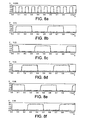
- Figure 8a to 8f represent the waveforms for the circuit of Figure 7.
- Figure 8a represents the input signal at a 50% duty cycle
- Figures 8b to 8e represent the output signals at each output node.
- Figure 9 illustrates how a programmable dividing circuit may be constructed to divide by a selected odd integer.
- Figure 9 illustrates a programmable dividing circuit which can selectively divide by three or by five.
- the transistor configuration of each stage S1 to S5 is not shown in Figure 9 but is the same as for Figure 7.
- a divide-by-five circuit is constructed as illustrated in Figure 7; however, instead of connecting the output of the last transistor stage S5 to the input of the first transistor stage S1 directly, the output V6 of the fifth transistor stage 5 is supplied to one input 4 of a multiplexer 6.
- the output V4 of the third transistor stage is supplied to the other input 2 of the multiplexer 6.
- An output 8 of the multiplexer 6 is connected to the input node of the first transistor stage S1 and also provides the output signal CLK OUT.
- a select input 10 receives a select signal SEL which controls whether the output V4 of the third transistor stage S3 or the output V6 of the fifth transistor stage S5 is supplied to the first transistor stage S1 and also serves as the output for the circuit. It will be appreciated that any suitable multiplexer could be used to selectively supply the output of the third or fifth stage as the input to the first transistor stage.
- Figure 10 illustrates operation of the circuit of Figure 9 with an input signal CLK IN having a 50% duty cycle as illustrated in Figure 10a.
- Figure 10b illustrates the state of the select signal SEL supplied to the select input 10 of the multiplexer 6.
- the select signal SEL is low, causing the first input 2 of the multiplexer 6 to be supplied to its output 8 and thus connecting in a ring the three transistor stages S1,S2 and S3.
- the circuit thus operates as a divide-by-three circuit, as can be seen from the output waveforms between time t0 and t1 in Figures 10c to 10h.
- the select signal SEL goes high, thus connecting the second input 4 to the output 8 of the multiplexer 6.
- the five transistor stages S1 to S5 are connected in a ring so that the circuit operates as a divide-by-five circuit, as can be seen from the waveforms in Figures 10c to 10h after time T1.
- FIG 11 is a diagram of a basic phase-locked-loop circuit in which the dividing circuits described herein are particularly useful.
- the phase-locked-loop receives a reference clock input REF CLK IN and generates a PLL clock output PLL CLK OUT.
- An input divider 50 creates from the reference clock input REF CLK IN a reference input frequency for a phase detector 52.
- the phase detector 52 also receives as an input a feedback signal ⁇ generated in a manner described in the following.
- An error output e is generated according to the relative phase of the reference signal and the feedback signal and is supplied to a charge pump 54.
- a loop filter 56 shapes the output of the charge pump 54 and generates a correction signal for a voltage controlled oscillator 58.
- the output of the voltage controlled oscillator is passed through a feedback divider 60 to generate the second input ⁇ to the phase detector.
- the output of the voltage controlled oscillator is also passed through an output divider 62 to generate the clock output PLL CLK
- a dividing circuit in accordance with the present invention can usefully be used to implement any of the input divider 50, feedback divider 60 or output divider 62 to provide a phase-locked-loop satisfying required technology, frequency and power constraints.
Landscapes
- Stabilization Of Oscillater, Synchronisation, Frequency Synthesizers (AREA)
- Manipulation Of Pulses (AREA)
Applications Claiming Priority (2)
| Application Number | Priority Date | Filing Date | Title |
|---|---|---|---|
| GB9727244 | 1997-12-23 | ||
| GBGB9727244.7A GB9727244D0 (en) | 1997-12-23 | 1997-12-23 | A dividing circuit and transistor stage therefor |
Publications (1)
| Publication Number | Publication Date |
|---|---|
| EP0926833A1 true EP0926833A1 (fr) | 1999-06-30 |
Family
ID=10824167
Family Applications (1)
| Application Number | Title | Priority Date | Filing Date |
|---|---|---|---|
| EP98310190A Withdrawn EP0926833A1 (fr) | 1997-12-23 | 1998-12-11 | Circuit diviseur et étage à transistor pour celui-ci |
Country Status (3)
| Country | Link |
|---|---|
| US (1) | US6208179B1 (fr) |
| EP (1) | EP0926833A1 (fr) |
| GB (1) | GB9727244D0 (fr) |
Cited By (3)
| Publication number | Priority date | Publication date | Assignee | Title |
|---|---|---|---|---|
| WO2010022092A1 (fr) * | 2008-08-18 | 2010-02-25 | Qualcomm Incorporated | Diviseur de fréquence en quadrature par trois |
| WO2010108037A1 (fr) * | 2009-03-19 | 2010-09-23 | Qualcomm Incorporated | Diviseur de fréquence avec sorties synchronisées |
| WO2010033855A3 (fr) * | 2008-09-19 | 2010-09-30 | Qualcomm Incorporated | Structure de verrou, diviseur de fréquence et procédés d'actionnement de ceux-ci |
Families Citing this family (4)
| Publication number | Priority date | Publication date | Assignee | Title |
|---|---|---|---|---|
| FR2847715B1 (fr) * | 2002-11-25 | 2005-03-11 | Commissariat Energie Atomique | Circuit integre comportant des sous-ensembles connectes en serie |
| KR100518226B1 (ko) * | 2003-04-23 | 2005-10-04 | 주식회사 하이닉스반도체 | Ddl 장치의 클락 분주기 및 그 클락 분주 방법 |
| US8344765B2 (en) * | 2009-07-16 | 2013-01-01 | Qualcomm, Incorporated | Frequency divider with a configurable dividing ratio |
| CN115149943B (zh) * | 2022-08-31 | 2022-11-22 | 上海韬润半导体有限公司 | 分频电路 |
Citations (7)
| Publication number | Priority date | Publication date | Assignee | Title |
|---|---|---|---|---|
| US3749937A (en) * | 1970-11-27 | 1973-07-31 | Smiths Industries Ltd | Electrical dividing circuits |
| US4389728A (en) * | 1979-12-29 | 1983-06-21 | Citizen Watch Co., Ltd. | Frequency divider |
| JPS6226920A (ja) * | 1985-07-29 | 1987-02-04 | Canon Inc | タイミング発生装置 |
| WO1990005413A1 (fr) * | 1988-10-31 | 1990-05-17 | Hughes Aircraft Company | Diviseur de frequence programmable numerique a haute vitesse |
| US4953187A (en) * | 1989-01-23 | 1990-08-28 | Motorola, Inc. | High speed prescaler |
| US5425074A (en) * | 1993-12-17 | 1995-06-13 | Intel Corporation | Fast programmable/resettable CMOS Johnson counters |
| EP0746109A1 (fr) * | 1995-05-31 | 1996-12-04 | STMicroelectronics S.A. | Diviseur programmable rapide |
Family Cites Families (5)
| Publication number | Priority date | Publication date | Assignee | Title |
|---|---|---|---|---|
| US4114049A (en) | 1972-02-25 | 1978-09-12 | Tokyo Shibaura Electric Co., Ltd. | Counter provided with complementary field effect transistor inverters |
| US4369379A (en) * | 1980-03-14 | 1983-01-18 | Texas Instruments Incorporated | CMOS Frequency divider circuit having invalid signal override |
| US4573176A (en) * | 1983-11-18 | 1986-02-25 | Rca Corporation | Fractional frequency divider |
| US4965531A (en) * | 1989-11-22 | 1990-10-23 | Carleton University | Frequency synthesizers having dividing ratio controlled by sigma-delta modulator |
| JPH07202649A (ja) * | 1993-12-27 | 1995-08-04 | Toshiba Corp | 逓倍回路 |
-
1997
- 1997-12-23 GB GBGB9727244.7A patent/GB9727244D0/en not_active Ceased
-
1998
- 1998-12-11 EP EP98310190A patent/EP0926833A1/fr not_active Withdrawn
- 1998-12-23 US US09/220,978 patent/US6208179B1/en not_active Expired - Lifetime
Patent Citations (7)
| Publication number | Priority date | Publication date | Assignee | Title |
|---|---|---|---|---|
| US3749937A (en) * | 1970-11-27 | 1973-07-31 | Smiths Industries Ltd | Electrical dividing circuits |
| US4389728A (en) * | 1979-12-29 | 1983-06-21 | Citizen Watch Co., Ltd. | Frequency divider |
| JPS6226920A (ja) * | 1985-07-29 | 1987-02-04 | Canon Inc | タイミング発生装置 |
| WO1990005413A1 (fr) * | 1988-10-31 | 1990-05-17 | Hughes Aircraft Company | Diviseur de frequence programmable numerique a haute vitesse |
| US4953187A (en) * | 1989-01-23 | 1990-08-28 | Motorola, Inc. | High speed prescaler |
| US5425074A (en) * | 1993-12-17 | 1995-06-13 | Intel Corporation | Fast programmable/resettable CMOS Johnson counters |
| EP0746109A1 (fr) * | 1995-05-31 | 1996-12-04 | STMicroelectronics S.A. | Diviseur programmable rapide |
Non-Patent Citations (2)
| Title |
|---|
| PATENT ABSTRACTS OF JAPAN vol. 011, no. 204 (E - 520) 2 July 1987 (1987-07-02) * |
| SUZUKI ET AL: "clocked cmos calculator circuitry", IEEE JOURNAL OF SOLID-STATE CIRCUITS., vol. sc-8, no. 6, December 1973 (1973-12-01), NEW YORK US, pages 462 - 469, XP002064533 * |
Cited By (10)
| Publication number | Priority date | Publication date | Assignee | Title |
|---|---|---|---|---|
| WO2010022092A1 (fr) * | 2008-08-18 | 2010-02-25 | Qualcomm Incorporated | Diviseur de fréquence en quadrature par trois |
| US7825703B2 (en) | 2008-08-18 | 2010-11-02 | Qualcomm Incorporated | Divide-by-three quadrature frequency divider |
| CN102124653A (zh) * | 2008-08-18 | 2011-07-13 | 高通股份有限公司 | 三分正交分频器 |
| CN102124653B (zh) * | 2008-08-18 | 2014-10-08 | 高通股份有限公司 | 三分正交分频器 |
| WO2010033855A3 (fr) * | 2008-09-19 | 2010-09-30 | Qualcomm Incorporated | Structure de verrou, diviseur de fréquence et procédés d'actionnement de ceux-ci |
| US8058901B2 (en) | 2008-09-19 | 2011-11-15 | Qualcomm Incorporated | Latch structure, frequency divider, and methods for operating same |
| US8519742B2 (en) | 2008-09-19 | 2013-08-27 | Qualcomm Incorporated | Latch structure, frequency divider, and methods for operating same |
| WO2010108037A1 (fr) * | 2009-03-19 | 2010-09-23 | Qualcomm Incorporated | Diviseur de fréquence avec sorties synchronisées |
| US8265568B2 (en) | 2009-03-19 | 2012-09-11 | Qualcomm Incorporated | Frequency divider with synchronized outputs |
| JP2012521669A (ja) * | 2009-03-19 | 2012-09-13 | クゥアルコム・インコーポレイテッド | 同期出力を有する周波数分周器 |
Also Published As
| Publication number | Publication date |
|---|---|
| GB9727244D0 (en) | 1998-02-25 |
| US6208179B1 (en) | 2001-03-27 |
Similar Documents
| Publication | Publication Date | Title |
|---|---|---|
| US6566918B1 (en) | Divide-by-N clock divider circuit with minimal additional delay | |
| US6917662B2 (en) | Programmable low-power high-frequency divider | |
| US6388492B2 (en) | Clock generation circuit | |
| US4953187A (en) | High speed prescaler | |
| KR970006394B1 (ko) | 다상 클럭 발생 회로 | |
| US10333397B2 (en) | Multi-stage charge pump circuit operating to simultaneously generate both a positive voltage and a negative voltage | |
| US10523211B2 (en) | Wide range glitchless switchable clock divider with modified 2/3 divider stages | |
| JP3601961B2 (ja) | デュアル・モジュラス・プリスケーラ | |
| JP2005536923A (ja) | 多相発振器およびそのための方法 | |
| US5221863A (en) | Phase-locked loop clock signal generator | |
| KR100724559B1 (ko) | 레벨 쉬프터 | |
| US6522711B2 (en) | Variable frequency divider circuit | |
| US6803799B1 (en) | Low power flip flop | |
| JP2024524968A (ja) | リング発振器に基づく分周器 | |
| EP0926833A1 (fr) | Circuit diviseur et étage à transistor pour celui-ci | |
| US20060280278A1 (en) | Frequency divider circuit with a feedback shift register | |
| US6967512B2 (en) | Multiphase-clock processing circuit and clock multiplying circuit | |
| US4715052A (en) | Frequency divide by N circuit | |
| US6154077A (en) | Bistable flip-flop | |
| EP0926834B1 (fr) | Circuit diviseur programmable | |
| US7038495B2 (en) | Low jitter high speed CMOS to CML clock converter | |
| US8466720B2 (en) | Frequency division of an input clock signal | |
| EP0926832B1 (fr) | Circuit diviseur pour diviser par des nombres pairs | |
| EP1469604B1 (fr) | Circuit generateur d'echelles a deux modules | |
| EP1856804A2 (fr) | Diviseur a faible bruit |
Legal Events
| Date | Code | Title | Description |
|---|---|---|---|
| PUAI | Public reference made under article 153(3) epc to a published international application that has entered the european phase |
Free format text: ORIGINAL CODE: 0009012 |
|
| AK | Designated contracting states |
Kind code of ref document: A1 Designated state(s): DE FR GB IT |
|
| AX | Request for extension of the european patent |
Free format text: AL;LT;LV;MK;RO;SI |
|
| 17P | Request for examination filed |
Effective date: 19991202 |
|
| AKX | Designation fees paid |
Free format text: DE FR GB IT |
|
| 17Q | First examination report despatched |
Effective date: 20040114 |
|
| STAA | Information on the status of an ep patent application or granted ep patent |
Free format text: STATUS: THE APPLICATION HAS BEEN WITHDRAWN |
|
| 18W | Application withdrawn |
Effective date: 20041220 |