EP0927986A1 - Treiber mit niedrigem Energieverbrauch für Flüssigkristallanzeige - Google Patents
Treiber mit niedrigem Energieverbrauch für Flüssigkristallanzeige Download PDFInfo
- Publication number
- EP0927986A1 EP0927986A1 EP99100077A EP99100077A EP0927986A1 EP 0927986 A1 EP0927986 A1 EP 0927986A1 EP 99100077 A EP99100077 A EP 99100077A EP 99100077 A EP99100077 A EP 99100077A EP 0927986 A1 EP0927986 A1 EP 0927986A1
- Authority
- EP
- European Patent Office
- Prior art keywords
- signal
- selecting
- signals
- liquid crystal
- crystal display
- Prior art date
- Legal status (The legal status is an assumption and is not a legal conclusion. Google has not performed a legal analysis and makes no representation as to the accuracy of the status listed.)
- Granted
Links
- 239000004973 liquid crystal related substance Substances 0.000 title claims abstract description 60
- 230000003111 delayed effect Effects 0.000 claims description 34
- 101150103877 Selenom gene Proteins 0.000 claims description 27
- 102100040428 Chitobiosyldiphosphodolichol beta-mannosyltransferase Human genes 0.000 claims description 26
- 101000891557 Homo sapiens Chitobiosyldiphosphodolichol beta-mannosyltransferase Proteins 0.000 claims description 26
- 230000003213 activating effect Effects 0.000 claims description 2
- 230000001902 propagating effect Effects 0.000 claims 2
- 230000007274 generation of a signal involved in cell-cell signaling Effects 0.000 claims 1
- 101100191136 Arabidopsis thaliana PCMP-A2 gene Proteins 0.000 description 30
- 101100048260 Saccharomyces cerevisiae (strain ATCC 204508 / S288c) UBX2 gene Proteins 0.000 description 30
- 101000891547 Homo sapiens Alpha-1,3/1,6-mannosyltransferase ALG2 Proteins 0.000 description 21
- 102100034785 Programmed cell death protein 6 Human genes 0.000 description 21
- 101000885321 Homo sapiens Serine/threonine-protein kinase DCLK1 Proteins 0.000 description 18
- 102100039758 Serine/threonine-protein kinase DCLK1 Human genes 0.000 description 18
- 102100031699 Choline transporter-like protein 1 Human genes 0.000 description 14
- 101000940912 Homo sapiens Choline transporter-like protein 1 Proteins 0.000 description 14
- 238000010586 diagram Methods 0.000 description 8
- 101000885387 Homo sapiens Serine/threonine-protein kinase DCLK2 Proteins 0.000 description 6
- 102100039775 Serine/threonine-protein kinase DCLK2 Human genes 0.000 description 6
- 230000008859 change Effects 0.000 description 6
- 230000007704 transition Effects 0.000 description 4
- 102100030341 Ethanolaminephosphotransferase 1 Human genes 0.000 description 3
- 101100172525 Homo sapiens SELENOI gene Proteins 0.000 description 3
- 101100422768 Saccharomyces cerevisiae (strain ATCC 204508 / S288c) SUL2 gene Proteins 0.000 description 3
- 239000011159 matrix material Substances 0.000 description 3
- 239000010409 thin film Substances 0.000 description 3
- 238000011084 recovery Methods 0.000 description 2
- 230000004044 response Effects 0.000 description 2
- 101150073246 AGL1 gene Proteins 0.000 description 1
- 102100035954 Choline transporter-like protein 2 Human genes 0.000 description 1
- 102100040844 Dual specificity protein kinase CLK2 Human genes 0.000 description 1
- 101000948115 Homo sapiens Choline transporter-like protein 2 Proteins 0.000 description 1
- 101000749291 Homo sapiens Dual specificity protein kinase CLK2 Proteins 0.000 description 1
- 239000003990 capacitor Substances 0.000 description 1
- 230000000295 complement effect Effects 0.000 description 1
- 238000007599 discharging Methods 0.000 description 1
- 230000004048 modification Effects 0.000 description 1
- 238000012986 modification Methods 0.000 description 1
- 230000003071 parasitic effect Effects 0.000 description 1
- 230000001105 regulatory effect Effects 0.000 description 1
- 239000004065 semiconductor Substances 0.000 description 1
Images





Classifications
-
- G—PHYSICS
- G09—EDUCATION; CRYPTOGRAPHY; DISPLAY; ADVERTISING; SEALS
- G09G—ARRANGEMENTS OR CIRCUITS FOR CONTROL OF INDICATING DEVICES USING STATIC MEANS TO PRESENT VARIABLE INFORMATION
- G09G3/00—Control arrangements or circuits, of interest only in connection with visual indicators other than cathode-ray tubes
- G09G3/20—Control arrangements or circuits, of interest only in connection with visual indicators other than cathode-ray tubes for presentation of an assembly of a number of characters, e.g. a page, by composing the assembly by combination of individual elements arranged in a matrix no fixed position being assigned to or needed to be assigned to the individual characters or partial characters
- G09G3/34—Control arrangements or circuits, of interest only in connection with visual indicators other than cathode-ray tubes for presentation of an assembly of a number of characters, e.g. a page, by composing the assembly by combination of individual elements arranged in a matrix no fixed position being assigned to or needed to be assigned to the individual characters or partial characters by control of light from an independent source
- G09G3/36—Control arrangements or circuits, of interest only in connection with visual indicators other than cathode-ray tubes for presentation of an assembly of a number of characters, e.g. a page, by composing the assembly by combination of individual elements arranged in a matrix no fixed position being assigned to or needed to be assigned to the individual characters or partial characters by control of light from an independent source using liquid crystals
-
- G—PHYSICS
- G09—EDUCATION; CRYPTOGRAPHY; DISPLAY; ADVERTISING; SEALS
- G09G—ARRANGEMENTS OR CIRCUITS FOR CONTROL OF INDICATING DEVICES USING STATIC MEANS TO PRESENT VARIABLE INFORMATION
- G09G3/00—Control arrangements or circuits, of interest only in connection with visual indicators other than cathode-ray tubes
- G09G3/20—Control arrangements or circuits, of interest only in connection with visual indicators other than cathode-ray tubes for presentation of an assembly of a number of characters, e.g. a page, by composing the assembly by combination of individual elements arranged in a matrix no fixed position being assigned to or needed to be assigned to the individual characters or partial characters
- G09G3/34—Control arrangements or circuits, of interest only in connection with visual indicators other than cathode-ray tubes for presentation of an assembly of a number of characters, e.g. a page, by composing the assembly by combination of individual elements arranged in a matrix no fixed position being assigned to or needed to be assigned to the individual characters or partial characters by control of light from an independent source
- G09G3/36—Control arrangements or circuits, of interest only in connection with visual indicators other than cathode-ray tubes for presentation of an assembly of a number of characters, e.g. a page, by composing the assembly by combination of individual elements arranged in a matrix no fixed position being assigned to or needed to be assigned to the individual characters or partial characters by control of light from an independent source using liquid crystals
- G09G3/3611—Control of matrices with row and column drivers
- G09G3/3674—Details of drivers for scan electrodes
- G09G3/3677—Details of drivers for scan electrodes suitable for active matrices only
-
- G—PHYSICS
- G09—EDUCATION; CRYPTOGRAPHY; DISPLAY; ADVERTISING; SEALS
- G09G—ARRANGEMENTS OR CIRCUITS FOR CONTROL OF INDICATING DEVICES USING STATIC MEANS TO PRESENT VARIABLE INFORMATION
- G09G2310/00—Command of the display device
- G09G2310/06—Details of flat display driving waveforms
-
- G—PHYSICS
- G09—EDUCATION; CRYPTOGRAPHY; DISPLAY; ADVERTISING; SEALS
- G09G—ARRANGEMENTS OR CIRCUITS FOR CONTROL OF INDICATING DEVICES USING STATIC MEANS TO PRESENT VARIABLE INFORMATION
- G09G2330/00—Aspects of power supply; Aspects of display protection and defect management
- G09G2330/02—Details of power systems and of start or stop of display operation
- G09G2330/021—Power management, e.g. power saving
- G09G2330/023—Power management, e.g. power saving using energy recovery or conservation
Definitions
- This invention relates to a liquid crystal display driver and, more particularly, to a liquid crystal display driver having a common line driver for sequentially driving common signal lines of a liquid crystal display panel.
- the prior art liquid crystal display driver 1 is associated with a liquid crystal display panel 2.
- the liquid crystal display panel 2 includes pixels P00, P01, ..., P0n, P10, P11, ..., P1n, ..., Pm0, Pm1, ... and Pmn arranged in matrix, common signal lines C0, C1, ..., Cm respectively associated with the rows of pixels P00 - P0n, P10 - P1n,..., Pm0 - Pmn and segment signal lines S0, S1,..., Sn respectively associated with the columns of pixels P00 - Pm0, P01 - Pm1, ..., P0n - Pmn.
- a thin film transistor and a piece of liquid crystal sandwiched between a pixel electrode and a part of a common electrode form in combination each of the pixels P00 to Pmn.
- the common signal line C0, C1.. or Cm is connected to the gate electrodes of the thin film transistors forming the associated row, and is sometimes called as "gate line”.
- the segment signal line S0, S1, .. or Sn is connected to the source nodes ofthe thin film transistors forming the associated column, and is sometimes called as "source line”.
- the prior art liquid crystal display driver 1 includes a common line driver 3, a segment line driver 4 and a control circuit 5.
- the common line driver 3 is connected to the common signal lines C0 to Cm, and sequentially supplies a common signal to the common signal lines C0 to Cm.
- the segment line driver 4 is connected to the segment signal lines S0 to Sn, and supplies segment signals representative of a part of image to be produced on a row of pixels to the segment signal lines S0 to Sn in synchronism with the. common signal.
- the common line driver 3 is supplying the common signal from the common signal line C0 to the common signal line Cm, the segment signals produces the image on the pixel matrix P00 to Pmn, and the time period for producing the image is called as "frame".
- the control circuit 5 is connected to the common line driver 3 and the segment line driver 4, and controls the image producing operation on the pixel matrix P00 to Pmn.
- the control circuit 5 supplies potential signals V1/ V2 and a selecting signal SEL to the common line driver 3, and the common line driver 3 generates the common signal Sc0/ Sc1/ ... / Scm at different timings.
- An image carrying signal IMG representative of the image is supplied to the control circuit 5, and the control circuit 5 instructs the segment line driver 4 to regulate each of the segment signals to an appropriate potential level.
- FIG. 2 illustrates the common line driver 3.
- the common line driver 3 consists of analog switching units SW0, SW1, ... and SWm, and each of the analog switching units SW0 to SWm is implemented by a pair of analog switches ALG1/ ALG2.
- the potential signal V1 and the other potential signal V2 are supplied to the analog switches ALG1 and the other analog switches ALG2, respectively.
- the pairs of analog switches ALG1/ ALG2 are connected to the common signal lines C0, C1,... and Cm, respectively, and are controlled with the selecting signal SEL.
- the selecting signal SEL consists of selecting sub-signals SEL0, SEL1,... and SELm, and the selecting sub-signals SEL0 to SELm are respectively supplied to the analog switching units SW0 to SWm, respectively.
- the control circuit 5 sequentially changes the selecting sub-signals SEL0 to SELm to active high level.
- the selecting sub-signals SEL0 to SELm are directly supplied to the analog switches ALG1, and the other analog switches ALG2 are supplied with the complementary signals thereof internally generated. For this reason, the analog switch ALG1 and the associated analog switch ALG2 complementarily turn on and off, and supplies the common signal Sc0/ Sc1/ .../ Scm to the associated common signal line C0/ C1/ .../ Cm.
- the prior art common line driver 3 behaves as illustrated in figure 3.
- Frame F1 is continued from time t0 to time t3
- frame F2 is continued from time t3 to time t6.
- the control circuit 5 regulates the potential signal V1 and the other potential signal V2 to potential level Va and potential level Vc in the frame F1, and sequentially changes the selecting sub-signals SEL0, SEL1, ... and SELm to active high level at time t0, time t1,... and time t2. While the control circuit 5 is maintaining one of the selecting sub-signals SEL0/ SEL1/ ../ SELm at the active high level, the other selecting sub-signals are maintained at inactive low level.
- the selecting sub-signals SEL0, SEL1, ... and SELm of the active high level cause the associated analog switches ALG1 to sequentially turn on, and the analog switching units SW0, SW1,....and SWm supply the common signal Sc0/ Sc1/.../Scm of the potential level Va to the associated common signal lines C0, C1, ... and Cm at time t0, time t1,... and time t2.
- the selecting sub-signals SEL0/ SEL1/.. SELm stay at the inactive low level, the analog switches ALG1 is turned off, and the associated analog switches ALG2 are turned on.
- only one common signal line C0, C1, .. or Cm is changed to the potential level Va, and the other common signal lines are maintained at the potential level Vc.
- the control circuit 5 regulates the potential signal V1 and the other potential signal V2 to potential level Vd and potential level Vb in the next frame F2, and sequentially changes the selecting sub-signals SEL0, SEL1, ... and SELm to the active level at time t3, time t4, ... and time t5.
- the selecting sub-signals SEL0, SEL1, ... and SELm are changed to the active high level at time t3, time t4,... and time t5, and cause the analog switches ALG1 to sequentially turn on.
- the other selecting sub-signals are maintained at the inactive low level, and the associated analog switches ALG2 are turned on.
- the common signal Sc0/ Sc1/.../ Scm changes the associated common signal line C0/ C1/ ... / Cm to the potential level Vd at time t3, time t4,... and time t5, and the other common signal lines are maintained at the potential level Vb.
- the prior art common line driver 3 alternates the common signal Sc0 to Scm between the potential range Va - Vc and the potential range Vd - Vb.
- the common signal Sc0 - Scm changes the active level between Va and Vd and the inactive level between Vc and Vb.
- the present inventor contemplated the problem, and noticed that each of the common signal lines C0/ C1/... Cm was independently charged and discharged.
- the control circuit 5 was expected to swing the common signal lines C0/C1/... Cm between the potential level Va/ Vd and the potential level Vc/ Vb, and consumed a large amount of electric power.
- the present inventor concluded that the common line driver 3 had to reuse the current discharged from the common signal line changed from the selected state to the non-selected state.
- a liquid crystal display driver associated with a liquid crystal display panel having a plurality of selecting lines for selectively activating pixels and a plurality of data lines for producing a piece of image on the activated pixels in each frame and comprising a control circuit sequentially changing preliminary selecting signals from an inactive level through an active level to the inactive level in each frame and a driving circuit connected between the control circuit and the plurality of selecting lines for selectively changing the plurality of selecting lines with driving signals sequentially changed to an active level and including a control signal generator defining a plurality of sub-frames respectively assigned to the plurality of selecting lines in the aforesaid each frame and generating a control signal in a first phase of each of the plurality of sub-frames and a selecting signal in a second phase of the aforesaid each of the plurality of sub-frames after the first phase and a switching array connected between the control signal generator and the plurality of selecting lines and responsive to the control signal for transferring electric charge between one
- a liquid crystal display driver 10 is connected to a liquid crystal display panel 11.
- the liquid crystal display panel 11 is similar to the liquid crystal display panel 2, and signal lines and pixels are labeled with the same references designating corresponding signal lines and corresponding pixels of the liquid crystal display panel without detailed description.
- the liquid crystal display driver 10 largely comprises a segment line driver 12, a control circuit 13 and a common line driver 14.
- the segment line driver 12 is connected to the segment signal lines S0 to Sn, and responsive to an instruction signal INS for generating segment signals SG0 to SGn representative of a piece of image to be produced on a row of pixels P00 - P0n, P10 - P1n, P20 - P2n, .... or Pm0 - Pmn.
- the segment signals SG0 to SGn are valid in a frame, and are changed from frame to frame.
- the segment line driver 12 is similar to that of the prior art liquid crystal display driver 1, and no further description is incorporated hereinbelow.
- the control circuit 13 sequentially changes preliminary selecting sub-signals SEL0, SEL1, SEL2, ... and SELm to the high active level, and generates the instruction signal INS in response to an image carrying signal IMG representative of the image to be produced on the pixel array POO to Pmn.
- the control circuit 13 is similar to that of the prior art liquid crystal display driver 1 except the potential signals V1/ V2, and no further description is incorporated hereinbelow.
- the common line driver 14 includes a control signal generator 15 and an analog switch array 16.
- the control signal generator 15 introduces delay time into the pulse fall of each preliminary selecting signal SEL0/ SEL1/../ SELm and the pulse rise of the next preliminary selecting signal, and generates selecting sub-signals DSEL0 to DSELm.
- the control signal generator 15 further generates control signals CTL0, CTL1, CTL2, ... and CTLm in the delay times, respectively, and, accordingly, each control signal CTL0/ CTL1/ ... / CTLm is followed by the associated control signal DSEL0/ DSEL1/ ... /DSELm.
- the selecting sub-signals DSEL0 to DSELm and the control signals CTL0 to CTLm are supplied from the control signal generator 15 to the analog switch array 16.
- the analog switch array 16 is connected to the control signal generator 15 and voltage supply lines V1/ V2.
- the analog switch array 16 is responsive to the control signals CTL0 to CTLm and the selecting sub-signals DSEL0 to DSELm for generating a common signal Sc0/ Sc1/ Sc2/ .../ Scm.
- the common signal Sc0/ Sc1/ Sc2 .../ Scm is sequentially supplied to the common signal lines C0, C1, C2, ... and Cm, and sequentially makes the rows of pixels P00 - P0n, P10 - P1n, P20 - P2n, .... and Pm0 - Pmn responsive to the segment signals SG0 to SGn.
- the analog switch array 16 causes each common signal line C0/ C1/ C2/ ...
- the common line driver 14 reuses the electric power, and the electric power consumption is reduced to a half of the electric power consumption of the prior art common line driver 3 by virtue of the preliminary charging/ discharging operation.
- FIG. 5 illustrates the control signal generator 15.
- the control signal generator 15 includes a timing generator 17, a delay circuit 18, a NOR gate 19, D-type flip flop circuits 20/ 21/.../ 22 and AND gates 23/24, 25/ 26,... 27/ 28.
- a clock signal CLK is supplied to an input node of the timing generator 17, and the timing generator 17 divides the clock signal CLK for generating timing signals TM1/ TM2.
- the timing signal TM1 is twice longer in clock period than the clock signal CLK, and the timing signal TM4 is four times longer in clock period than the clock signal CLK.
- the clock signal CLK is further supplied to an input node of the delay circuit 18, and the delay circuit 18 produces a delayed clock signal DCLK from the clock signal CLK.
- the delayed clock signal DCLK at the low level is partially overlapped with the clock signal CLK at the low level.
- the clock signal CLK, the timing signals TM1/ TM2 and the delayed clock signal DCLK are supplied to the four input nodes of the NOR gate 19, and the NOR gate 19 yields a timing signal TM3.
- the preliminary selecting sub-signals SEL0 - SELm are respectively supplied to the data nodes D of the D-type flip flop circuits 20 - 22, and the delayed clock signal DCLK is supplied to the clock nodes C of the D-type flip flop circuits 20 - 22.
- Each D-type flip flop circuit 20/ 21/ .../ 22 stores the voltage level of the associated preliminary selecting sub-signal SEL0/ SEL1/ .../ SELm at the pulse rise of the delayed clock signal DCLK, and changes the voltage level at the output node Q.
- the preliminary selecting sub-signals SEL0 - SELm are respectively supplied to the first input nodes of the AND gates 23/ 25/ .../ 27, and the output signals of the D-type flip flop circuits 20 - 22 are respectively supplied to the second input nodes of the AND gates 23/ 25/ ... / 27. For this reason, the when both of the associated preliminary selecting sub-signal SEL0/ SEL1/ .../ SELm and the associated output signal are in the high level, the AND gate 23/ 25/ .../ 27 changes the selecting sub-signal DSEL0/ DSEL1/ ... / DSELm to the high level.
- the preliminary selecting sub-signals SEL0/ SEL1/ .../ SELm are respectively supplied to the first input nodes ofthe AND gates 24/ 26/ .../ 28, and the timing signal TM3 is supplied to all the second input nodes of the AND gates 24/ 26/ ... / 28. For this reason, while the timing signal TM3 is staying at the high level, the AND gate 24/ 26/ .../ 28 transfers the preliminary selecting sub-signal SEL0/ SEL1/ ..../ SELm of the high level to the output node thereof so as to change the control signal CTL0/ CTL1/ ..../ CTLm to the high level.
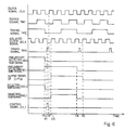
- Figure 5 illustrates the circuit behavior of the control signal generator 15. Although the illustration is focused on the generation of the selecting sub-signal DSEL1 and the control signal CTL1, the other selecting sub-signals and the other control signals are generated at different timings as similar to the selecting sub-signal DSEL1 and the control signal CTL1.
- the preliminary selecting sub-signal SEL0 is changed to the low level at time t10, and the next preliminary selecting sub-signal SELI is immediately changed to the high level.
- the preliminary selecting sub-signal SEL0 causes the AND gate 23 to change the selecting sub-signal DSEL0 to the low level.
- the AND gate 25 maintains the selecting sub-signal DSEL1 in the low level.
- the delayed clock signal DCLK is changed to the low level at time t11.
- the clock signal CLK and the timing signals TM1/ TM2 have been changed to the low level before time t11, and all the input nodes of the NOR gate 19 are in the low level at time t11. For this reason, the NOR gate 19 changes the timing signal TM3 to the high level, and maintains the timing signal TM3 in the high level until time t12.
- the clock signal CLK is changed to the high level at time t12, and the NOR gate 19 changes the timing signal TM3 to the low level at time t12.
- the AND gate 26 is responsive to the timing signal TM3 at the high level, and changes the control signal CTL1 to the high level.
- the AND gate 26 maintains the control signal CTL1 in the high level until time t12, and changes the control signal CTL1 to the low level at time t12.
- the delayed clock signal DCLK is changed to the high level at time t13 for the first time after the change of the preliminary selecting sub-signal SELI to the high level, and the D-type flip flop circuit 21 latches the high level of the preliminary sub-selecting signal SELI at the leading edge of the delayed clock signal DCLK. Then, the D-type flip flop circuit 21 changes the output node Q to the high level, and the AND gate 25 changes the selecting sub-signal DSEL1 to the high level at time t13.
- the preliminary selecting sub-signal SEL1 is changed to the low level at time t14, and the delayed clock signal DCLK is changed to the high level at time t15 for the first time after the fall of the preliminary selecting sub-signal SEL1.
- the D-type flip flop circuit 21 latches the low level of the preliminary selecting sub-signal SEL1, and changes the output node Q to the low level.
- control signal generator 15 firstly changes the control signal CTL0/ CTL1/ ... / CTLm to the high level, and the associated selecting sub-signal DSEL0/ DSEL1/ .../ DSELm to the high level after the recovery of the control signal.
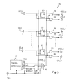
- FIG. 7 illustrates the analog switch array 16.
- the analog switch array 16 includes analog switching units 29/ 30/ .../ 31, bypass switches 32/ 33/ .../ 34 and a current path 35.
- the bypass switches 32/ 33/ .../ 34 are implemented by analog switches, respectively.
- the current path 35 is looped, and the bypass switches 32/ 33/ .../ 34 are inserted into the current path 35 at intervals.
- the common signal lines C0/ C1/ .../ Cm are connected between the bypass switches 32, 33, .... 34 and 32, and the bypass switches 32/ 33/ ... / 34 are respectively controlled with the control signals CTL0/ CTL1/ ... / CTLm.
- the analog switching units 29/ 30/ .../ 31 are respectively implemented by pairs of analog switches ALG1/ ALG2, and the selecting sub-signals DSEL0/ DSEL1/ ... /DSELm are supplied to the analog switching units 29/ 30/ .../ 31, respectively.
- the analog switching units 29/ 30/ .../ 31 invert the selecting sub-signals DSEL0/ DSEL1/ ... DSELm, and the selecting sub-signals DSEL0 to DSELm and the inverted signals are supplied to the analog switches ALG1 and the associated analog switches ALG2, respectively.
- a short delay time is introduced between the potential change of the selecting sub-signal DSEL0/ DSEL1/ .../ DSELm and the potential change of the inverted signal thereof.
- the analog switch ALG1 turns on.
- the inverted signal of the high level causes the analog switch ALG2 to turn on.
- the voltage supply line V1 is connected to the input nodes of all the analog switches ALG1, and the other voltage supply line V2 is connected to the input nodes of the other analog switches ALG2.
- the output nodes of the analog switching units 29/ 30/.../ 31 are connected to the current path 35 between the bypass switches 32, 33, ..., 34 and 32.
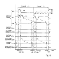
- Figure 8 illustrates a sequential selection of the common signal lines C0 to Cm.
- Frame F1 is followed by the next frame F2, and the frames F1 and F2 are continued from time t20 to time t26 and from time t26 to time t32, respectively.
- the common line driver 14 While the common line driver 14 is operating in the frame F1, the voltage supply line V1 supplies potential level Va to the analog switches ALG1, and the voltage supply line V2 supplies potential level Vc to the analog switches ALG2.
- the potential level Vc is lower than the potential level Va.
- the voltage supply lines V1/ V2 are changed to potential level Vd and potential level Vb, respectively, in the next frame F2.
- the potential level Vb is regulated between the potential level Va and the potential level Vc, and the potential level Vd is lower than the potential level Vc.
- the control signals CTL0, CTL1, ... and CTLm are sequentially changed to the active high level at time t20, time t22,... and time t24 in the frame F1, and cause the bypass switches 32, 33, ... and 34 to turn on.
- the control signals CTL0, CTL1,... and CTLm are recovered to the inactive low level before time t21, time t23, ... and time t25. While the control signal CTL0/ CTL1/ .../ CTLm is staying at the active high level, the associated bypass switch 32/ 33/ ... /34 electrically connects the common signal line Cm/ C1/ ..../ Cm-1 to the next common signal line C1/ C2/... / Cm, and the potential level on the common signal line Cm/C1/ .../ Cm-1 is equalized to the potential level on the next common signal line C1/ C2/..../ Cm.
- the selecting sub-signals DSEL0, DSEL1, ... and DSELm are sequentially changed to the active high level at time t21, time t23, ... and time t25.
- the selecting sub-signal DSEL0/ DSEL1/ .../ DSELm at the active high level causes the analog switch AGL1 of the associated analog switching unit 29/ 30/ ..../ 31 to turn on, and the analog switch ALG2 of the associated analog switching unit 29/ 30/ .../ 31 to turn off.
- selecting sub-signals DSEL0, DSEL1 and DSELm at the active high level cause the associated analog switching units 29, 30, ... and 31 to sequentially supply the common signal Sc0/ Sc1/.../ Scm to the common signal lines C0, C1, ...
- the selecting sub-signals DSEL0, DSEL1, ....and DSELm at the inactive low level causes the associated analog switching units 29, 30, ...and 31 to electrically connect the other voltage supply line V2 to the common signal lines C0, C1, ....and Cm.
- the control signal generator 15 changes the control signal CTL1 to the active high level at time t22, and the bypass switch 33 turns on.
- the other bypass switches 32, ....and 34 are turned off, and the common signal line C0 is electrically connected through the bypass switch 33 to the common signal line C1. Electric charge flows from the common signal line C0 to the common signal line C1, and the common signal lines C0 and C1 are equalized at potential level Vm (see common signal Sc0 and Sc1 between time t22 and time t23).
- the control signal generator 15 changes the selecting sub-signal DSEL1 to the active high level at time t23, and the voltage supply line V1 raises the common signal line C1 to the potential level Va.
- the inverted signal of the selecting sub-signal DSEL0 causes the analog switch ALG2 of the analog switching unit 20 to turn on, and the common signal line C0 goes down to the potential level Vc.
- the control circuit changes the preliminary selecting sub-signal SEL1 and the next preliminary selecting sub-signal to the low level and the high level, respectively, the electric charge firstly flows from the common signal line C1 to the next common signal line C2, and, thereafter, the voltage supply line V1 pulls up the common signal line C2 to the potential level Va.
- the bypass switches 32 to 34 also sequentially transfer the electric charge to the next common signal lines, and the electric power consumption is reduced.
- Equation 1 The amount of electric charge Q accumulated on the common signal line C0 to Cm is expressed by equation 1.
- Q C ( Va - Vc) where C is the capacitance of a parasitic capacitor coupled to the common signal line.
- the potential difference ( Va - Vm) is equal to the potential difference ( Vm - Vc).
- Each of the potential differences ( Va - Vm) and ( Vm - Vc) is assumed to be corresponding to Qm.
- the common signal line C0 to Cm supplies half of the electric charge to be required for the next common signal line, and the electric power consumption is reduced to a half of the electric power consumption of the prior art common line driver.
- the common signal lines C0 to Cm partially charges the next common signal lines C1 to C0 through the bypass switches 32 to 34, and the common line driver 14 is improved in electric power consumption.
- each sub-frame is, by way of example, corresponding to the time period between time t20 and time t22, and the first phase and the second phase of the sub-frame is continued from time t20 to time t21 and from time t21 to time t22, respectively.
- a common line driver 41 is connected to the common signal lines C0, C1, C2...and Cm of the liquid crystal display panel 11.
- the common line driver 41 is incorporated in another liquid crystal display driver 42 embodying the present invention.
- the common line driver 41 comprises a control signal generator 43 and an analog switch array 44, and the control circuit 13 supplies the preliminary control sub-signals SEL0/ SEL1/ SEL2..../ SELm to the control signal generator 43 as similar to the first embodiment.
- the preliminary selecting sub-signals SEL0 - SELm and a clock signal CLK are supplied to the control signal generator 43.
- the control signal generator 43 produces selecting sub-signals DSEL10, DSEL11, DSEL12, ...and DSELlm from the preliminary selecting sub-signals SEL0/ SEL1/ ....SEL2/ ...and SELm.
- the control signal generator 43 retards the pulse fall of the selecting sub-signal DSEL10/ DSEL11/ DSEL12/.../ DSELm from the pulse rise of the next selecting sub-signal DSEL11/ DSEL12/.../ DSELm/ DSEL10, and makes the selecting sub-signal DSEL10/ DSEL11/ DSEL12/ .../ DSEL1m partially overlapped in the high level with the next selecting sub-signal DSEL11/DSEL12/.../ DSEL1m/ DSEL10...
- the control signal generator 43 further produces a control signal CTL20, and the control signal CTL20 is changed to an active low level before the pulse fall of the selecting sub-signal DSEL10/ DSEL11/ DSEL12/.../ DSELm.
- the control signal generator 43 maintains the control signal CTL20 in the active low level for a short while, and recovers the control signal CTL20 to an inactive high level after the pulse rise of the next selecting sub-signal DSEL11/ DSEL12/..../ DSEL1m/ DSEL10.
- the selecting sub-signals DSEL10 - DSEL1m and the control signal CTL20 are supplied to the analog switch array 44.
- the analog switch array 44 is responsive to the control signal CTL20 so as to flow electric charge from a selected common signal line C0/ C1/ C2/..../ Cm to the next selected common signal line C1/ C2/..../ Cm/ C0. After the recovery of the control signal CTL20 to the inactive high level, the analog switch array 44 connects the voltage supply line V1 to the next selected common signal line C1/ C2/.../ Cm/ C0. Thus, the next selected common signal line C1/ C2/ .../ Cm/ C0 is firstly charged by the previously selected common signal line C0/ C1/ C2/../ Cm, and, thereafter, the voltage supply line V1 charges the next common signal line C1/ C2/ .../ Cm/ C0. As a result, the electric power consumption is reduced.
- FIG 10 illustrates the control signal generator 43.
- the control signal generator 43 is broken down into two units 45/ 46.
- the first unit 45 produces delayed clock signals DCLK1/ DCLK2 from the clock signal CLK and the control signal CTL20 from the clock signal CLK and the delayed clock signal DCLK2.
- the second unit latches the preliminary selecting sub-signals SEL0 - SELm in response to the delayed clock signal DCLK1, and produces the selecting sub-signals DSEL0 - DSELm from the preliminary selecting sub-signals SEL0 - SELm and the latched signals.
- the first unit 45 includes an inverter 47 supplied with the clock signal CLK, delay circuits 48/ 49 connected in series to the inverter 47 for producing the delayed clock signal DCLK1, a delay circuit 50 connected to the delay circuit 49 for producing the delayed clock signal DCLK2 and an OR gate supplied with the clock signal CLK and the delayed clock signal DCLK2 for producing the control signal CTL20.
- the delayed clock signals DCLK0, DCLK1 and DCLK2 have respective pulse falls F0/ F1/ F2 successively delayed from the pulse rise Rx of the clock signal CLK, and the pulse rises R0/ R1/ R2 are successively delayed from the pulse fall Fx.
- the clock signal CLK falls at time t40, and the delayed clock signals DCLK0/ DCLK1/ DCLK2 respectively rise at time t42, time t43 and time t44.
- the clock signal CLK is ORed with the delayed clock signal CLK2, and the first unit 45 maintains the control signal CTL20 in the active low level from time t40 to time t44.
- the second unit 46 includes D-type flip flop circuits 52/ 53/.../ 54 and OR gates 55/ 56/.../ 57.
- the preliminary selecting sub-signals SEL0/ SEL1/..../ SELm are respectively supplied to the data input nodes D of the D-type flip flop circuits 55/ 56/.../ 57, and the delayed clock signal DCLK1 is supplied to the clock nodes of the D-type flip flop circuits 55/ 56/..../ 57.
- the preliminary selecting sub-signals SEL0 - SELm are respectively supplied to the first input nodes of the OR gates 55/ 56/.../ 57, and the output signals of the D-type flip flop circuits 52/ 53/..../ 54 are supplied to the second input nodes of the OR gates 55/ 56/ ..../ 57, respectively.
- the D-type flip flop circuits 52-54 latch potential levels at the data input nodes D at the pulse rise of the delayed clock signal DCLK1, and maintain the potential levels until the next pulse rise regardless of the potential change at the data input nodes D.
- the D-type flip flop circuit 52/ 53..../ 54 introduces delay time between the pulse fall of the associated preliminary selecting sub-signal SEL0/ SEL1/ ..../ SELm and the pulse fall of the selecting sub-signal DSEL10/ DSEL11/..../ DSEL1m.
- the control circuit changes the preliminary selecting sub-signal SEL0 from the high level to the low level at time t41, and concurrently changes the next preliminary selecting sub-signal SEL1 from the low level to the high level (see figure 11).
- the preliminary selecting sub-signal SEL0 is supplied to the data input node of the D-type flip flop circuit 52 and the first input node of the OR gate 55
- the next preliminary selecting sub-signal SEL1 is supplied to the data input node of the D-type flip flop circuit 53 and the first input node of the OR gate 56.
- the pulse rise of the preliminary selecting sub-signal SEL1 immediately affects the selecting sub-signal DSEL11 through the OR gate 56, and the next selecting sub-signal DSEL11 is changed to the high level at time t41.
- the D-type flip flop circuit 53 have latched the high level of the preliminary selecting sub-signal SEL0, and maintains the output node Q in the high level until the next pulse rise ofthe delayed clock signal DCLK1.
- the delayed clock signal DCLK1 rises at time t43, and the D-type flip flop circuit 53 latches the low level of the preliminary selecting sub-signal SEL1.
- the D-type flip flop circuit 53 immediately changes the output node Q to the low level, and, accordingly, the OR gate 56 changes the selecting sub-signal DSEL11 to the low level at time t43.
- the preliminary selecting sub-signal DSEL11 is overlapped in the high level with the preliminary selecting sub-signal DSEL10 between time t41 to time t43, and the overlap is nested in the active low level of the control signal CTL20.
- FIG 12 illustrates the analog switch array 44.
- the analog switch array 44 includes analog switching units 58/ 59/.... /60 and two analog switches 61/ 62.
- a parallel combination of analog switches ALG1/ ALG2 forms the analog switching unit 58/ 59/ Vietnamese/ 60.
- the voltage supply line V1 is connected through the analog switch 61 to the analog switches ALG1, and the other voltage supply line V2 is connected through the analog switch 62 to the analog switches ALG2.
- the analog switching units 58/ 59/.../ 60 are respectively associated with the common signal lines C0/ C1/.../ Cm, and the analog switches ALG1/ ALG2 of each unit 58/ 59/.../ 60 are connected to the associated common signal line C0/ C1/whereas/ Cm.
- the selecting sub-signals DSEL10/ DSEL11/ .../ DSELlm are respectively supplied to the analog switching units 58/ 59/.../ 60, and the analog switching units 58/ 59/..../ 60 invert the selecting sub-signals DSEL10/ DSEL11/.... /DSEL1m.
- the selecting sub-signals DSEL10/ DSEL11/ ..../ DSELlm and the inverted signals thereof are supplied to the analog switches ALG1 and the analog switches ALG2, respectively.
- analog switching units 58/ 59/ .../ 60 are selectively connect the voltage supply lines V1/ V2 to the common signal lines C0/ C1/.../ Cm depending upon the potential level of the associated selecting sub-signals DSEL10/ DSEL11/ ..../ DSEL1m.
- the control signal CTL20 is supplied to the analog switches 61/ 62. While the control signal CTL20 is staying at the inactive high level, the analog switches 61/ 62 are turned on, and allows the voltage supply lines V1/ V2 to supply the potentials thereon to the analog switches ALG1/ ALG2. On the other hand, the control signal CTL20 of the active low level renders the analog switches 61/ 62 off, and the analog switches ALG1/ ALG2 are electrically isolated from the voltage supply lines V1/ V2.
- the common signal line C0/ C1/.../ Cm is electrically connected through the associated analog switches ALG1 to the adjacent common signal line C1/.../ Cm/ C0, because the associated selecting sub-signals are concurrently in the high level for a short while. Thereafter, the voltage supply line V1 supplies the potential through the analog switch 61 and the analog switch ALG1 to the adjacent common signal line C1/ .../ Cm/ C0.
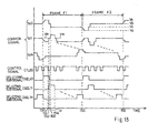
- Figure 13 illustrates the circuit behavior of the common line driver 41 under the same conditions as the common line driver 14.
- Frames F1/ F2 are continued from time t50 to time t55 and from time t55 to time t56, respectively.
- the potential levels Va/ Vc are respectively supplied to the voltage supply lines V1/ V2 in the frame F1, and the voltage supply lines V1/ V2 are respectively changed to the potential level Vd and the potential level Vb, in the next frame F2.
- the common signals Sc0/ Sc1/..../ Scm are sequentially changed to the potential level Va, and, thereafter, each common signal Sc0 - Scm is decayed to the potential level Vc in the frame F1.
- the common signals Sc0/ Sc1/.../ Scm are sequentially decayed to the potential level Vd, and, thereafter, each common signal Sc0 - Scm rises to the potential level Vb.
- the common signals Sc0/ Sc1/.../ Scm are sequentially supplied to the associated common signal lines C0/ C1/..../ Cm.
- description is made on the transition from the common signal line C0 to the next common signal line C1 in the frame F1 for the sake of simplicity.
- the other transition is analogous to the transition from the common signal line C0 to the next common signal line C1.
- the clock signal CLK is changed to the high level before time t51, and the control signal CTL20 falls to the active low level at time t51.
- the control signal generator 43 keeps the control signal CTL20 at the active low level between time t51 and time t54.
- the control signal CTL20 is recovered to the inactive high level at time t54.
- the preliminary selecting sub-signal SEL0 is changed to the low level at time t52, and the next preliminary selecting sub-signal SEL1 is immediately changed to the high level.
- the preliminary selecting sub-signal SEL1 immediately affects the selecting sub-signal DSEL11, and the selecting sub-signal DSEL11 is changed to the high level at time t52.
- the selecting sub-signal DSEL10 is maintained in the high level for a short while, and falls to the low level at time t53.
- both selecting sub-signals DSEL10/ DSEL11 are concurrently in the high level between time t52 and time t53.
- the time period between time t52 and time t53 is nested in the time period from time t51 to time t54.
- control signal CTL20 is changed to the inactive high level at time t54, and the voltage supply lines V1/ V2 supplies the potentials Va and Vc through the analog switch ALG1 of the switching unit 59 and the analog switch ALG2 of the switching unit 58 to the common signal line C1 and the common signal line C0, respectively.
- the common signals Sc0/ Sc1 are changed to the potential level Va and the potential level Vc, respectively.
- the circuit components of the common line driver 41 are less than those of the common line driver 14, and achieve all the advantages of the common line driver 14.
- one of the plurality of sub-frames is, by way of example, corresponding to the time period between time t51 and time t54, and the first phase and the second phase of the sub-frame are continued from time t51 to time t54 and from time t54 to the pulse fall of the selecting sub-signal DSEL11 at time tx.
- the particular feature of the present invention is directed to the control sequence of the common line driver 14/ 41 where the common line driver firstly charges a selected common signal line by using the previously selected common signal line and, thereafter, the potential line V1. The electric charge accumulated on the selected common signal line is reused for the next selected common signal line, and the electric power consumption is reduced.
- the potential signals may be internally generated.
- the external potential signals are not supplied to the liquid crystal display driver, and the clock signal CLK may be internally produced.
- the liquid crystal display driver may be integrated on a single semiconductor chip.
- the control signal CTL20 may be supplied to the analog switch 61, only.
- the other analog switch 62 may be deleted from the analog switch array.
Landscapes
- Engineering & Computer Science (AREA)
- Chemical & Material Sciences (AREA)
- Crystallography & Structural Chemistry (AREA)
- Physics & Mathematics (AREA)
- Computer Hardware Design (AREA)
- General Physics & Mathematics (AREA)
- Theoretical Computer Science (AREA)
- Liquid Crystal Display Device Control (AREA)
- Control Of Indicators Other Than Cathode Ray Tubes (AREA)
- Liquid Crystal (AREA)
Applications Claiming Priority (2)
| Application Number | Priority Date | Filing Date | Title |
|---|---|---|---|
| JP00041398A JP3150098B2 (ja) | 1998-01-05 | 1998-01-05 | 液晶駆動装置 |
| JP41398 | 1998-01-05 |
Publications (2)
| Publication Number | Publication Date |
|---|---|
| EP0927986A1 true EP0927986A1 (de) | 1999-07-07 |
| EP0927986B1 EP0927986B1 (de) | 2004-06-23 |
Family
ID=11473122
Family Applications (1)
| Application Number | Title | Priority Date | Filing Date |
|---|---|---|---|
| EP99100077A Expired - Lifetime EP0927986B1 (de) | 1998-01-05 | 1999-01-05 | Treiber mit niedrigem Energieverbrauch für Flüssigkristallanzeige |
Country Status (6)
| Country | Link |
|---|---|
| US (1) | US6300930B1 (de) |
| EP (1) | EP0927986B1 (de) |
| JP (1) | JP3150098B2 (de) |
| KR (1) | KR100330951B1 (de) |
| CN (1) | CN1131457C (de) |
| DE (1) | DE69918192T2 (de) |
Cited By (2)
| Publication number | Priority date | Publication date | Assignee | Title |
|---|---|---|---|---|
| EP1381015A3 (de) * | 2002-07-11 | 2004-11-17 | Seiko Epson Corporation | Elektrooptische Vorrichtung, Steuervorrichtung und -verfahren für eine elektrooptische Vorrichtung, und elektronisches Gerät |
| CN100452665C (zh) * | 2000-08-23 | 2009-01-14 | 株式会社半导体能源研究所 | 便携式信息设备以及驱动该设备的方法 |
Families Citing this family (13)
| Publication number | Priority date | Publication date | Assignee | Title |
|---|---|---|---|---|
| JP2001034237A (ja) * | 1999-07-21 | 2001-02-09 | Fujitsu Ltd | 液晶表示装置 |
| JP2002221939A (ja) * | 2001-01-24 | 2002-08-09 | Hitachi Ltd | 液晶表示装置 |
| JP2003029719A (ja) * | 2001-07-16 | 2003-01-31 | Hitachi Ltd | 液晶表示装置 |
| JP3820379B2 (ja) * | 2002-03-13 | 2006-09-13 | 松下電器産業株式会社 | 液晶駆動装置 |
| JP2004046066A (ja) * | 2002-05-17 | 2004-02-12 | Sharp Corp | 信号出力装置および表示装置 |
| CN100412630C (zh) * | 2002-07-11 | 2008-08-20 | 精工爱普生株式会社 | 电光器件及其驱动装置、驱动方法和电子装置 |
| CN100505013C (zh) * | 2002-10-25 | 2009-06-24 | Nxp股份有限公司 | 利用电荷共享的显示装置及其控制方法 |
| US7791575B2 (en) * | 2005-07-15 | 2010-09-07 | Solomon Systech Limited | Circuit for driving display panel with transition control |
| KR100666642B1 (ko) * | 2005-09-15 | 2007-01-09 | 삼성에스디아이 주식회사 | 주사 구동부 및 이를 포함하는 유기 전계발광 표시장치 |
| US7465934B2 (en) * | 2005-09-30 | 2008-12-16 | Eastman Kodak Company | Pixel array output routing structure for multi-channel CMOS imager sensors |
| JP2008116917A (ja) * | 2006-10-10 | 2008-05-22 | Seiko Epson Corp | ゲートドライバ、電気光学装置、電子機器及び駆動方法 |
| JP6763715B2 (ja) * | 2016-07-11 | 2020-09-30 | ローム株式会社 | タイミングコントローラ、その制御方法、それを用いた電子機器 |
| CN106875911B (zh) * | 2017-04-12 | 2019-04-16 | 京东方科技集团股份有限公司 | 移位寄存器单元、栅极驱动电路及其驱动方法 |
Citations (3)
| Publication number | Priority date | Publication date | Assignee | Title |
|---|---|---|---|---|
| EP0631271A1 (de) * | 1993-06-28 | 1994-12-28 | Sharp Kabushiki Kaisha | Anzeigevorrichtung mit aktiver Matrix und Speicherkondensatoren |
| US5528256A (en) * | 1994-08-16 | 1996-06-18 | Vivid Semiconductor, Inc. | Power-saving circuit and method for driving liquid crystal display |
| GB2326013A (en) * | 1997-05-31 | 1998-12-09 | Lg Semicon Co Ltd | Gate driver circuit for LCD |
Family Cites Families (8)
| Publication number | Priority date | Publication date | Assignee | Title |
|---|---|---|---|---|
| JPH05232904A (ja) * | 1992-02-18 | 1993-09-10 | Mitsubishi Electric Corp | 液晶表示装置 |
| TW277129B (de) * | 1993-12-24 | 1996-06-01 | Sharp Kk | |
| US5844534A (en) * | 1993-12-28 | 1998-12-01 | Kabushiki Kaisha Toshiba | Liquid crystal display apparatus |
| US5739804A (en) * | 1994-03-16 | 1998-04-14 | Kabushiki Kaisha Toshiba | Display device |
| JP2743841B2 (ja) * | 1994-07-28 | 1998-04-22 | 日本電気株式会社 | 液晶表示装置 |
| CN1129887C (zh) * | 1994-12-26 | 2003-12-03 | 夏普公司 | 液晶显示装置 |
| JP2822911B2 (ja) * | 1995-03-23 | 1998-11-11 | 日本電気株式会社 | 駆動回路 |
| JP3586998B2 (ja) | 1996-10-31 | 2004-11-10 | ソニー株式会社 | 液晶ディスプレイの駆動装置 |
-
1998
- 1998-01-05 JP JP00041398A patent/JP3150098B2/ja not_active Expired - Fee Related
-
1999
- 1999-01-04 US US09/224,795 patent/US6300930B1/en not_active Expired - Lifetime
- 1999-01-04 KR KR1019990000033A patent/KR100330951B1/ko not_active Expired - Fee Related
- 1999-01-05 EP EP99100077A patent/EP0927986B1/de not_active Expired - Lifetime
- 1999-01-05 DE DE69918192T patent/DE69918192T2/de not_active Expired - Fee Related
- 1999-01-05 CN CN99100011A patent/CN1131457C/zh not_active Expired - Fee Related
Patent Citations (3)
| Publication number | Priority date | Publication date | Assignee | Title |
|---|---|---|---|---|
| EP0631271A1 (de) * | 1993-06-28 | 1994-12-28 | Sharp Kabushiki Kaisha | Anzeigevorrichtung mit aktiver Matrix und Speicherkondensatoren |
| US5528256A (en) * | 1994-08-16 | 1996-06-18 | Vivid Semiconductor, Inc. | Power-saving circuit and method for driving liquid crystal display |
| GB2326013A (en) * | 1997-05-31 | 1998-12-09 | Lg Semicon Co Ltd | Gate driver circuit for LCD |
Cited By (3)
| Publication number | Priority date | Publication date | Assignee | Title |
|---|---|---|---|---|
| CN100452665C (zh) * | 2000-08-23 | 2009-01-14 | 株式会社半导体能源研究所 | 便携式信息设备以及驱动该设备的方法 |
| EP1381015A3 (de) * | 2002-07-11 | 2004-11-17 | Seiko Epson Corporation | Elektrooptische Vorrichtung, Steuervorrichtung und -verfahren für eine elektrooptische Vorrichtung, und elektronisches Gerät |
| US7091966B2 (en) | 2002-07-11 | 2006-08-15 | Seiko Epson Corporation | Electro-optical device, drive device and drive method for electro-optical device, and electronic apparatus |
Also Published As
| Publication number | Publication date |
|---|---|
| CN1224180A (zh) | 1999-07-28 |
| DE69918192D1 (de) | 2004-07-29 |
| JP3150098B2 (ja) | 2001-03-26 |
| DE69918192T2 (de) | 2005-06-30 |
| JPH11194314A (ja) | 1999-07-21 |
| KR19990067712A (ko) | 1999-08-25 |
| KR100330951B1 (ko) | 2002-04-01 |
| US6300930B1 (en) | 2001-10-09 |
| CN1131457C (zh) | 2003-12-17 |
| EP0927986B1 (de) | 2004-06-23 |
Similar Documents
| Publication | Publication Date | Title |
|---|---|---|
| EP0927986B1 (de) | Treiber mit niedrigem Energieverbrauch für Flüssigkristallanzeige | |
| CN115731839B (zh) | 显示驱动电路及显示装置 | |
| RU2473977C1 (ru) | Схема возбуждения для линий сканирующего сигнала, сдвиговый регистр и способ возбуждения сдвигового регистра | |
| JP5232956B2 (ja) | 液晶表示装置 | |
| US7460634B2 (en) | Shift register circuit | |
| US20080219401A1 (en) | Shift register circuit and image display apparatus containing the same | |
| US20060145999A1 (en) | Shift register | |
| US6954192B2 (en) | Source driver output circuit of thin film transistor liquid crystal display | |
| US11263988B2 (en) | Gate driving circuit and display device using the same | |
| CN105810170A (zh) | 移位寄存器单元及其驱动方法、栅线驱动电路和阵列基板 | |
| CN106875911A (zh) | 移位寄存器单元、栅极驱动电路及其驱动方法 | |
| JP2008537275A (ja) | シフトレジスタ回路 | |
| WO2006100637A2 (en) | A shift register circuit | |
| EP1911037B1 (de) | Multi-input-kreis | |
| US20060132182A1 (en) | Driver circuit, shift register, and liquid crystal driver circuit | |
| US7145540B2 (en) | Display device with variable-bias driver | |
| JP2006127751A (ja) | 同じ極性を有するmisトランジスタを用いるシフトレジスタの改良 | |
| CN218384465U (zh) | 一种栅极驱动电路及显示装置 | |
| CN114038386A (zh) | 栅极驱动器及显示装置 | |
| US7099166B2 (en) | Voltage boosting circuit and method | |
| US5212474A (en) | Quasi-static level shifter | |
| KR102625976B1 (ko) | 안정적으로 다중 주파수에서의 동작이 가능한 게이트 드라이버 | |
| KR100590934B1 (ko) | 액정표시장치용 쉬프트 레지스터 | |
| EP0456311B1 (de) | Quasi-statischer Pegelumsetzer | |
| JP3999212B2 (ja) | 表示装置及びその駆動方法 |
Legal Events
| Date | Code | Title | Description |
|---|---|---|---|
| PUAI | Public reference made under article 153(3) epc to a published international application that has entered the european phase |
Free format text: ORIGINAL CODE: 0009012 |
|
| AK | Designated contracting states |
Kind code of ref document: A1 Designated state(s): DE FR GB |
|
| AX | Request for extension of the european patent |
Free format text: AL;LT;LV;MK;RO;SI |
|
| 17P | Request for examination filed |
Effective date: 19990526 |
|
| AKX | Designation fees paid |
Free format text: DE FR GB |
|
| 17Q | First examination report despatched |
Effective date: 20011129 |
|
| RAP1 | Party data changed (applicant data changed or rights of an application transferred) |
Owner name: NEC ELECTRONICS CORPORATION |
|
| GRAP | Despatch of communication of intention to grant a patent |
Free format text: ORIGINAL CODE: EPIDOSNIGR1 |
|
| GRAA | (expected) grant |
Free format text: ORIGINAL CODE: 0009210 |
|
| GRAS | Grant fee paid |
Free format text: ORIGINAL CODE: EPIDOSNIGR3 |
|
| AK | Designated contracting states |
Kind code of ref document: B1 Designated state(s): DE FR GB |
|
| REG | Reference to a national code |
Ref country code: GB Ref legal event code: FG4D |
|
| REF | Corresponds to: |
Ref document number: 69918192 Country of ref document: DE Date of ref document: 20040729 Kind code of ref document: P |
|
| ET | Fr: translation filed | ||
| PLBE | No opposition filed within time limit |
Free format text: ORIGINAL CODE: 0009261 |
|
| STAA | Information on the status of an ep patent application or granted ep patent |
Free format text: STATUS: NO OPPOSITION FILED WITHIN TIME LIMIT |
|
| 26N | No opposition filed |
Effective date: 20050324 |
|
| PGFP | Annual fee paid to national office [announced via postgrant information from national office to epo] |
Ref country code: DE Payment date: 20061229 Year of fee payment: 9 |
|
| PGFP | Annual fee paid to national office [announced via postgrant information from national office to epo] |
Ref country code: GB Payment date: 20070103 Year of fee payment: 9 |
|
| PGFP | Annual fee paid to national office [announced via postgrant information from national office to epo] |
Ref country code: FR Payment date: 20070109 Year of fee payment: 9 |
|
| GBPC | Gb: european patent ceased through non-payment of renewal fee |
Effective date: 20080105 |
|
| PG25 | Lapsed in a contracting state [announced via postgrant information from national office to epo] |
Ref country code: DE Free format text: LAPSE BECAUSE OF NON-PAYMENT OF DUE FEES Effective date: 20080801 |
|
| REG | Reference to a national code |
Ref country code: FR Ref legal event code: ST Effective date: 20081029 |
|
| PG25 | Lapsed in a contracting state [announced via postgrant information from national office to epo] |
Ref country code: GB Free format text: LAPSE BECAUSE OF NON-PAYMENT OF DUE FEES Effective date: 20080105 |
|
| PG25 | Lapsed in a contracting state [announced via postgrant information from national office to epo] |
Ref country code: FR Free format text: LAPSE BECAUSE OF NON-PAYMENT OF DUE FEES Effective date: 20080131 |