EP0928024A2 - Amélioration des voies conductrices d'interconnexion - Google Patents
Amélioration des voies conductrices d'interconnexion Download PDFInfo
- Publication number
- EP0928024A2 EP0928024A2 EP99200003A EP99200003A EP0928024A2 EP 0928024 A2 EP0928024 A2 EP 0928024A2 EP 99200003 A EP99200003 A EP 99200003A EP 99200003 A EP99200003 A EP 99200003A EP 0928024 A2 EP0928024 A2 EP 0928024A2
- Authority
- EP
- European Patent Office
- Prior art keywords
- layer
- forming
- conducting
- conducting paths
- over
- Prior art date
- Legal status (The legal status is an assumption and is not a legal conclusion. Google has not performed a legal analysis and makes no representation as to the accuracy of the status listed.)
- Withdrawn
Links
Images


Classifications
-
- H—ELECTRICITY
- H10—SEMICONDUCTOR DEVICES; ELECTRIC SOLID-STATE DEVICES NOT OTHERWISE PROVIDED FOR
- H10W—GENERIC PACKAGES, INTERCONNECTIONS, CONNECTORS OR OTHER CONSTRUCTIONAL DETAILS OF DEVICES COVERED BY CLASS H10
- H10W70/00—Package substrates; Interposers; Redistribution layers [RDL]
- H10W70/01—Manufacture or treatment
- H10W70/04—Manufacture or treatment of leadframes
-
- H—ELECTRICITY
- H10—SEMICONDUCTOR DEVICES; ELECTRIC SOLID-STATE DEVICES NOT OTHERWISE PROVIDED FOR
- H10W—GENERIC PACKAGES, INTERCONNECTIONS, CONNECTORS OR OTHER CONSTRUCTIONAL DETAILS OF DEVICES COVERED BY CLASS H10
- H10W20/00—Interconnections in chips, wafers or substrates
- H10W20/01—Manufacture or treatment
- H10W20/071—Manufacture or treatment of dielectric parts thereof
- H10W20/081—Manufacture or treatment of dielectric parts thereof by forming openings in the dielectric parts
- H10W20/084—Manufacture or treatment of dielectric parts thereof by forming openings in the dielectric parts for dual-damascene structures
- H10W20/086—Manufacture or treatment of dielectric parts thereof by forming openings in the dielectric parts for dual-damascene structures involving buried masks
-
- H—ELECTRICITY
- H10—SEMICONDUCTOR DEVICES; ELECTRIC SOLID-STATE DEVICES NOT OTHERWISE PROVIDED FOR
- H10W—GENERIC PACKAGES, INTERCONNECTIONS, CONNECTORS OR OTHER CONSTRUCTIONAL DETAILS OF DEVICES COVERED BY CLASS H10
- H10W20/00—Interconnections in chips, wafers or substrates
- H10W20/01—Manufacture or treatment
- H10W20/031—Manufacture or treatment of conductive parts of the interconnections
- H10W20/064—Manufacture or treatment of conductive parts of the interconnections by modifying the conductivity of conductive parts, e.g. by alloying
- H10W20/065—Manufacture or treatment of conductive parts of the interconnections by modifying the conductivity of conductive parts, e.g. by alloying by making at least a portion of the conductive part non-conductive, e.g. by oxidation
-
- H—ELECTRICITY
- H10—SEMICONDUCTOR DEVICES; ELECTRIC SOLID-STATE DEVICES NOT OTHERWISE PROVIDED FOR
- H10W—GENERIC PACKAGES, INTERCONNECTIONS, CONNECTORS OR OTHER CONSTRUCTIONAL DETAILS OF DEVICES COVERED BY CLASS H10
- H10W20/00—Interconnections in chips, wafers or substrates
- H10W20/01—Manufacture or treatment
- H10W20/031—Manufacture or treatment of conductive parts of the interconnections
- H10W20/067—Manufacture or treatment of conductive parts of the interconnections by modifying the pattern of conductive parts
-
- H—ELECTRICITY
- H10—SEMICONDUCTOR DEVICES; ELECTRIC SOLID-STATE DEVICES NOT OTHERWISE PROVIDED FOR
- H10W—GENERIC PACKAGES, INTERCONNECTIONS, CONNECTORS OR OTHER CONSTRUCTIONAL DETAILS OF DEVICES COVERED BY CLASS H10
- H10W20/00—Interconnections in chips, wafers or substrates
- H10W20/40—Interconnections external to wafers or substrates, e.g. back-end-of-line [BEOL] metallisations or vias connecting to gate electrodes
- H10W20/41—Interconnections external to wafers or substrates, e.g. back-end-of-line [BEOL] metallisations or vias connecting to gate electrodes characterised by their conductive parts
- H10W20/42—Vias, e.g. via plugs
-
- H—ELECTRICITY
- H10—SEMICONDUCTOR DEVICES; ELECTRIC SOLID-STATE DEVICES NOT OTHERWISE PROVIDED FOR
- H10W—GENERIC PACKAGES, INTERCONNECTIONS, CONNECTORS OR OTHER CONSTRUCTIONAL DETAILS OF DEVICES COVERED BY CLASS H10
- H10W20/00—Interconnections in chips, wafers or substrates
- H10W20/40—Interconnections external to wafers or substrates, e.g. back-end-of-line [BEOL] metallisations or vias connecting to gate electrodes
- H10W20/495—Capacitive arrangements or effects of, or between wiring layers
-
- H—ELECTRICITY
- H10—SEMICONDUCTOR DEVICES; ELECTRIC SOLID-STATE DEVICES NOT OTHERWISE PROVIDED FOR
- H10W—GENERIC PACKAGES, INTERCONNECTIONS, CONNECTORS OR OTHER CONSTRUCTIONAL DETAILS OF DEVICES COVERED BY CLASS H10
- H10W72/00—Interconnections or connectors in packages
-
- H—ELECTRICITY
- H10—SEMICONDUCTOR DEVICES; ELECTRIC SOLID-STATE DEVICES NOT OTHERWISE PROVIDED FOR
- H10P—GENERIC PROCESSES OR APPARATUS FOR THE MANUFACTURE OR TREATMENT OF DEVICES COVERED BY CLASS H10
- H10P14/00—Formation of materials, e.g. in the shape of layers or pillars
- H10P14/40—Formation of materials, e.g. in the shape of layers or pillars of conductive or resistive materials
- H10P14/46—Formation of materials, e.g. in the shape of layers or pillars of conductive or resistive materials using a liquid
- H10P14/47—Electrolytic deposition, i.e. electroplating; Electroless plating
-
- Y—GENERAL TAGGING OF NEW TECHNOLOGICAL DEVELOPMENTS; GENERAL TAGGING OF CROSS-SECTIONAL TECHNOLOGIES SPANNING OVER SEVERAL SECTIONS OF THE IPC; TECHNICAL SUBJECTS COVERED BY FORMER USPC CROSS-REFERENCE ART COLLECTIONS [XRACs] AND DIGESTS
- Y10—TECHNICAL SUBJECTS COVERED BY FORMER USPC
- Y10T—TECHNICAL SUBJECTS COVERED BY FORMER US CLASSIFICATION
- Y10T29/00—Metal working
- Y10T29/49—Method of mechanical manufacture
- Y10T29/49002—Electrical device making
- Y10T29/49117—Conductor or circuit manufacturing
- Y10T29/49124—On flat or curved insulated base, e.g., printed circuit, etc.
- Y10T29/4913—Assembling to base an electrical component, e.g., capacitor, etc.
- Y10T29/49144—Assembling to base an electrical component, e.g., capacitor, etc. by metal fusion
-
- Y—GENERAL TAGGING OF NEW TECHNOLOGICAL DEVELOPMENTS; GENERAL TAGGING OF CROSS-SECTIONAL TECHNOLOGIES SPANNING OVER SEVERAL SECTIONS OF THE IPC; TECHNICAL SUBJECTS COVERED BY FORMER USPC CROSS-REFERENCE ART COLLECTIONS [XRACs] AND DIGESTS
- Y10—TECHNICAL SUBJECTS COVERED BY FORMER USPC
- Y10T—TECHNICAL SUBJECTS COVERED BY FORMER US CLASSIFICATION
- Y10T29/00—Metal working
- Y10T29/49—Method of mechanical manufacture
- Y10T29/49002—Electrical device making
- Y10T29/49117—Conductor or circuit manufacturing
- Y10T29/49124—On flat or curved insulated base, e.g., printed circuit, etc.
- Y10T29/49147—Assembling terminal to base
- Y10T29/49149—Assembling terminal to base by metal fusion bonding
-
- Y—GENERAL TAGGING OF NEW TECHNOLOGICAL DEVELOPMENTS; GENERAL TAGGING OF CROSS-SECTIONAL TECHNOLOGIES SPANNING OVER SEVERAL SECTIONS OF THE IPC; TECHNICAL SUBJECTS COVERED BY FORMER USPC CROSS-REFERENCE ART COLLECTIONS [XRACs] AND DIGESTS
- Y10—TECHNICAL SUBJECTS COVERED BY FORMER USPC
- Y10T—TECHNICAL SUBJECTS COVERED BY FORMER US CLASSIFICATION
- Y10T29/00—Metal working
- Y10T29/49—Method of mechanical manufacture
- Y10T29/49002—Electrical device making
- Y10T29/49117—Conductor or circuit manufacturing
- Y10T29/49124—On flat or curved insulated base, e.g., printed circuit, etc.
- Y10T29/49147—Assembling terminal to base
- Y10T29/49151—Assembling terminal to base by deforming or shaping
Definitions
- This invention relates generally to integrated semiconductor circuits and, more particularly, to the conducting leads or interconnect paths that carry electrical signals between electronic components.
- the metal stack forming the conducting paths should be thick to reduce the lead resistance and reduce the voltage drop along the conducting path.
- the metal stack should be thin to reduce the parasitic capacitance. The width of the metal stacks is typically minimised to provide a maximum density of components for the integrated circuit.
- the solution for providing conducting paths for both types, of signals has been to provide a metal stack of a thickness that is a compromise between a desirable capacitance parameter and a desirable resistance parameter.
- metal stacks of a predetermined thickness.
- the selected metal stacks can then have conductive material added to selected stacks or can have conducting material removed from selected metal stacks.
- Added conducting material can be implemented, for example, by electrolytic deposition of conducting material on a stack, or by chemical or vapor deposition of conducting material on metal stacks not covered by protective material.
- Conducting material can be removed from selective stacks by, for example, et ching material from metal stacks not covered by a protective material.
- the metal stacks can have a stop layer or can be comprised of two selectively etchable materials so that the removal of material can be controlled.
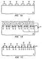
- a technique for controlling the relative capacitance/resistance parameters for selected conducting paths is shown.
- a plurality of conducting paths 12 are formed on a dielectric material 11. These conducting paths 12 have approximately the same , thickness.
- Dielectric sidewalls 13 are formed on the sides of the conducting paths in Fig. 1B by deposition and anisotropic etchback.
- an electrolytic material 19 including ions, atoms and/or molecules consistent with the material of the conducting paths 12 is applied over the conducting paths 12, the sidewalls 13 and the dielectric material 11 in Fig. 1B.
- the electrolytic material can be a liquid, a gas, or a slurry, as appropriate.
- a potential difference (i.e., resulting from the coupling of power supply 14) is established between the electrolytic material 19 and selected conducting leads 12. This potential difference results in the deposition of (conducting) material from the electrolytic material on the conducting paths 12 resulting, as shown in Fig. 1C, in additional conducting material 15 on the exposed conducting surface of the selected conducting paths 12.
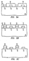
- a second technique, for adding material to selected, conducting paths 13 is shown.
- the non-selected, conducting paths 12 are covered with a protective material 25 as shown in Fig. 2A.
- the conducting paths 12 have sidewalls 13 formed thereon.
- a liquid or gas carrier material 29, (including ions, atoms or other conducting particles that will attach to the conducting material of which the conducting paths 12 are comprised) is applied to the surface of the protective material 25, to the exposed surface of dielectric material 11, to the exposed surface of the sidewall material 13 and to the exposed surfaces of the selected conducting paths 12.
- the conducting material of carrier material 29 will be selectively attached to the exposed portion of the conducting paths 12. Not only are the exposed portions of the non-selected conducting. paths 29 isolated from the conducting material of carrier material 29. but any conducting material attached to the protective material 25 will be removed when the protective material is removed. The selected conducting paths 12 will therefore be enlarged by the added conducting material 15.
- Figs. 3A-3C illustrate another implementation of the technique wherein conducting material is added to selected conducting paths 12 to control the relative resistance/parasitic capacitance of conducting paths 12.
- the conducting paths 12 have been formed on a dielectric substrate.
- a ,IS@ photoresist layer 31 has been formed and patterned to expose the selected conducting paths 12.
- conducting material 15 is electroplated on the exposed portions of the conducting paths 12.
- the photoresist layer 31 is removed and the normal conducting paths 12 and the selected conducting paths 12/is are exposed for further processing.
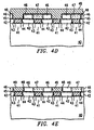
- a single flow damascene technique for providing a controllable thickness for conducting paths in a semiconductor device conducting path layer.
- patterned dielectric layer 42 is formed on a dielectric layer 40.
- the pattern formation includes cavities and/or channels that will be vias or the selected, conducting paths in the dielectric layer 46.
- the dotted lines represent conducting vias 41 that have been formed in the dielectric layer 40.
- a thin containment layer 43 is formed over the exposed surfaces and a, for example, copper layer 44 is formed over the containment layer.
- conducting paths 44 are formed in the dielectric material 42 as shown in Fig. 4C, In Fig.
- an etch stop layer 45 is applied to-the surface formed by the chemical/mechanical processing operation shown in Fig. 4C.
- a ⁇ dielectric layer 46 is then formed and patterned, and the etch stop layer removed at the bottom of the cavities in the dielectric layer 46 thereby exposing the conducting leads 44.
- a thin containment layer 48 is applied to the exposed surfaces.
- a copper layer 49 is formed over the containment layer 48.
- a second chemical/mechanical operation provides a surface in preparation for further polishing.
- conducting paths 49 are electrically coupled to conducting paths 44 providing the selected, thicker conducting paths for the metal layer.
- the vias 47 (illustrated by dotted lines) provide electrical contact to the is non-selected (and thinner) conducting paths.
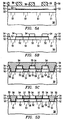
- a technique for selected conducting path enhancement using a dual damascene process is illustrated.
- an dielectric layer 52 is deposited on a semiconductor integrated circuit layer 50.
- a dielectric etch stop layer 53 is formed over the dielectric layer 52.
- the dielectric etch stop layer 53 has channel paths (indicated by the missing portions of the layer 53) and via paths (indicated by dotted lines in layer 53) formed therein. These channel and via paths in the dielectric etch stop layer 53 are positioned in relationship to vias 51 in the layer 50.
- a second dielectric layer 54 is formed over the dielectric etch stop layer 53 and the exposed portions of the oxide layer 52.
- a photo resist layer 59 is formed and patterned, In Fig.
- the result of etching the dielectric layer 54 exposed by the patterned photo resist layer 59 is shown.
- the dielectric material of layer 54 is removed by the etching process down to the dielectric etch stop layer 53.
- the etching process continues through dielectric layer 52 to layer 50.
- Fig. 5C the exposed surfaces of layers 50, 52, 53, and 54 are covered with a thin containment layer 55, and the containment layer 55 is covered with a copper layer 56.
- a surface is formed exposing the selected (thick) conducting paths 56 and the non-selected conducting paths 57.
- the non-selected conducting paths 57 can be coupled to layer 50 by vias (shown with dotted lines).
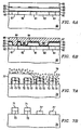
- a damascene technique for increasing the thickness of a portion of a conducting path in is a metal layer is shown.
- a plurality of conducting paths 61. in a first metal layer extend perpendicular to the plane of the drawing.
- Dielectric material 62 is found between the conducting paths 61.
- An etch stop layer 63 is positioned over the dielectric material 62 and the etch stop layer 61.
- a dielectric layer 64 is positioned over the dielectric layer 64.
- a patterned etch stop layer 65 is Formed over the dielectric layer 64.
- the patterns in etch stop layer 65 are positioned directly above the conducting paths 61 to which a via is to be extended and are otherwise positioned to be directly above regions of dielectric material 62.
- Dielectric material 66 is formed above the etch stop layer 65 and the exposed regions of dielectric layer 64.
- a channel, perpendicular to conducting paths 61 is etched in dielectric layer 64. The etching extends through the patterns in etch stop layer 65 to etch stop layer 63.
- a containment layer 67 is then formed over the exposed surfaces of etch stop layer 62, dielectric layer 64, etch stop laver 62, and the walls of dielectric layer 66 (not indicated).
- a copper layer 68 is formed over the containment layer 67.
- the conducting path 68 has a via electrically coupling conducting path 61', and a group of thickened regions 68' associated with the conducting path 68 of an upper metal layer.
- a series of conducting paths 71 extends perpendicular to the plane of the drawing.
- the conducting paths 71 have sidewalls 72 associated therewith.
- a protective is material 77 is formed over the selected conducting paths 71.
- An etching solution or gas 79 is then applied to the exposed areas.
- the protective material 77 prevents the etching solution from affecting the conducting paths 71 thereunder, but the exposed conducting paths 71 have material removed therefrom.
- the amount of material removed can be a function of the time the conducting paths 71 or, optionally, a conducting etch stop layer 73 can be included in the conducting path 71 (i.e. to determine the amount of material removed from the conducting path).
- the protective material 77 and the sidewalls 72 have been removed to leave the selected conducting paths 71 thicker than the non-selected conducting paths 71'.
- a method for fabricating conducting paths between electronic components in an integrated circuit comprising the steps of: forming conducting paths between the electronic components; and adding conducting material to selected conducting paths.
- removable material is applied over non-selected conducting paths during the adding step.
- the adding step is implemented by electrolytic deposition on conducting material over the selected conducting paths.
- a method for fabricating conducting paths between components in and integrated circuit comprising the steps of: forming conducting paths between the electronic components; and removing conducting material from selected conducting paths.
- the method includes the step of fabricating the conducting paths to include a etch stop conducting layer between. two conducting path layers.
- An integrated circuit comprising: a plurality of electronic components; and a multiplicity of conducting paths electrically coupling the plurality of electronic components, wherein' selected metal stacks forming the conducting paths are thicker than non-selected metal stacks.
- the thicker metal stacks are formed by adding conducting material to the selected stacks.
- the thicker metal stacks are formed by removing conducting material from the non-selected metal stacks.
- An integrated circuit comprising: a plurality of electronic components; and at least one layer having a multiplicity of conducting paths, wherein selected ones of the multiplicity of conducting paths having a greater thickness than non-selected conducting paths.
- a method for augmenting the thickness of selected conductors in a metal layer of an integrated circuit comprising the steps of: patterning a dielectric layer to form a first group of channels therein; forming containment layer over exposed portions of the dielectric layer and a bottom material exposed by the patterning step; forming a layer of copper over the containment layer, the layer of copper filling the group of channels; forming a first surface by chemical/mechanical processing of the metal layer, the first surface exposing alternative areas of the layer of copper in the first group of channels separated by areas of the dielectric layer; forming an etch stop layer on the first surface; forming and patterning a second dielectric layer on the etch stop layer, the patterning forming a second group of channels opposite selected ones of the first group of channels separated by the etch stop layer; removing the etch stop layer exposed by the patterning step of the second dielectric layer; after depositing a second containment layer over exposed surfaces of the dielectric layer and first surface layer, forming a second copper layer over the second containment layer, the
- the second patterning step includes forming wells opposite predetermined ones of the first group of channels, the well providing vias to the predetermined channels after the remaining steps.
- An integrated semiconductor circuit comprising: a plurality of active semiconductor components; and at least one metal layer electrically coupling preselected ones of the active semiconductor components, the metal layer including a plurality of conducting paths, wherein at least one selected conducting path is made thicker than other conducting paths.
- a method of thickening selected conducting paths in a metal layer comprising the steps of: forming a first dielectric layer on first layer; forming and patterning channel in an etch stop layer, patterns is the etch stop layer determined by where channels are to extend to the first layer; forming a second dielectric layer on the etch stop layer; forming and patterning photoresist layer over the second dielectric layer; etching channels in the second dielectric layer determined by the photoresist layer to form non-selected channels, wherein selected channels in the second dielectric layer extend through the etch stop layer and through the first dielectric layer; forming a containment layer over exposed surfaces formed as a result of the etching steps; forming a copper layer over the containment layer, the copper layer filling the channels; and forming a surface exposing copper areas separated by areas of the second dielectric layer.
- the conducting paths and the selected conducting paths of the metal layer are perpendicular to conducting paths in the first layer.
- An integrated semiconductor circuit comprising: a plurality of active semiconductor components; and a metal layer having a plurality of conducting paths, wherein selected conducting paths are made thicker than the remaining conducting paths.
- thickness and, therefore, the relative resistance/capacitance of conducting paths in an integrated circuit can be controlled.
- This control can provide an enhancement of the performance of an integrated circuit by providing a reduced resistance or a reduced capacitance for selected conducting paths while still remaining within the design parameters for the width of the conducting paths.
Landscapes
- Internal Circuitry In Semiconductor Integrated Circuit Devices (AREA)
- Electrodes Of Semiconductors (AREA)
- Parts Printed On Printed Circuit Boards (AREA)
Applications Claiming Priority (2)
| Application Number | Priority Date | Filing Date | Title |
|---|---|---|---|
| US7044398P | 1998-01-05 | 1998-01-05 | |
| US70443P | 1998-01-05 |
Publications (2)
| Publication Number | Publication Date |
|---|---|
| EP0928024A2 true EP0928024A2 (fr) | 1999-07-07 |
| EP0928024A3 EP0928024A3 (fr) | 2002-12-04 |
Family
ID=22095316
Family Applications (1)
| Application Number | Title | Priority Date | Filing Date |
|---|---|---|---|
| EP99200003A Withdrawn EP0928024A3 (fr) | 1998-01-05 | 1999-01-05 | Amélioration des voies conductrices d'interconnexion |
Country Status (4)
| Country | Link |
|---|---|
| US (1) | US6169664B1 (fr) |
| EP (1) | EP0928024A3 (fr) |
| JP (1) | JPH11251321A (fr) |
| KR (1) | KR100591236B1 (fr) |
Cited By (2)
| Publication number | Priority date | Publication date | Assignee | Title |
|---|---|---|---|---|
| WO2001078135A3 (fr) * | 2000-03-24 | 2002-02-21 | Nutool Inc | Procedes pour reparer des defectuosites sur un substrat semi-conducteur |
| WO2003021684A1 (fr) * | 2001-09-04 | 2003-03-13 | Koninklijke Philips Electronics N.V. | Procede pour produire un dispositif a semi-conducteur avec structure de bord |
Families Citing this family (3)
| Publication number | Priority date | Publication date | Assignee | Title |
|---|---|---|---|---|
| JP4249360B2 (ja) * | 1999-11-02 | 2009-04-02 | 日東電工株式会社 | 回路基板およびその製造方法 |
| JP2004063610A (ja) * | 2002-07-26 | 2004-02-26 | Seiko Instruments Inc | 半導体装置の製造方法 |
| JP2004063996A (ja) * | 2002-07-31 | 2004-02-26 | Matsushita Electric Ind Co Ltd | 半導体装置及びその製造方法 |
Family Cites Families (28)
| Publication number | Priority date | Publication date | Assignee | Title |
|---|---|---|---|---|
| US4447291A (en) * | 1983-08-31 | 1984-05-08 | Texas Instruments Incorporated | Method for via formation in HgCdTe |
| US4805683A (en) * | 1988-03-04 | 1989-02-21 | International Business Machines Corporation | Method for producing a plurality of layers of metallurgy |
| US5070392A (en) * | 1988-03-18 | 1991-12-03 | Digital Equipment Corporation | Integrated circuit having laser-alterable metallization layer |
| US5038996A (en) * | 1988-10-12 | 1991-08-13 | International Business Machines Corporation | Bonding of metallic surfaces |
| EP0411165B1 (fr) * | 1989-07-26 | 1997-04-02 | International Business Machines Corporation | Procédé de fabrication d'une structure d'empaquetage pour puce à circuit intégré |
| US5256274A (en) * | 1990-08-01 | 1993-10-26 | Jaime Poris | Selective metal electrodeposition process |
| US5151168A (en) * | 1990-09-24 | 1992-09-29 | Micron Technology, Inc. | Process for metallizing integrated circuits with electrolytically-deposited copper |
| US5148143A (en) * | 1991-04-12 | 1992-09-15 | Beltone Electronics Corporation | Precision thick film elements |
| JPH05160292A (ja) * | 1991-06-06 | 1993-06-25 | Toshiba Corp | 多層パッケージ |
| US5227013A (en) * | 1991-07-25 | 1993-07-13 | Microelectronics And Computer Technology Corporation | Forming via holes in a multilevel substrate in a single step |
| US5282312A (en) * | 1991-12-31 | 1994-02-01 | Tessera, Inc. | Multi-layer circuit construction methods with customization features |
| JP2773578B2 (ja) * | 1992-10-02 | 1998-07-09 | 日本電気株式会社 | 半導体装置の製造方法 |
| US5490324A (en) * | 1993-09-15 | 1996-02-13 | Lsi Logic Corporation | Method of making integrated circuit package having multiple bonding tiers |
| US5428339A (en) * | 1993-11-01 | 1995-06-27 | Intermedics, Inc. | Trimmable resistors with reducible resistance and method of manufacture |
| FR2713397B1 (fr) * | 1993-12-03 | 1996-02-16 | Sgs Thomson Microelectronics | Procédé de formation de couches métalliques minces et épaisses. |
| US5461003A (en) * | 1994-05-27 | 1995-10-24 | Texas Instruments Incorporated | Multilevel interconnect structure with air gaps formed between metal leads |
| WO1996008037A1 (fr) * | 1994-09-06 | 1996-03-14 | Sheldahl, Inc. | Substrat de circuit imprime equipe directement de puces de circuits integres sans boitier et procede de fabrication |
| US5635423A (en) * | 1994-10-11 | 1997-06-03 | Advanced Micro Devices, Inc. | Simplified dual damascene process for multi-level metallization and interconnection structure |
| US5487218A (en) * | 1994-11-21 | 1996-01-30 | International Business Machines Corporation | Method for making printed circuit boards with selectivity filled plated through holes |
| US5534462A (en) * | 1995-02-24 | 1996-07-09 | Motorola, Inc. | Method for forming a plug and semiconductor device having the same |
| US5557502A (en) * | 1995-03-02 | 1996-09-17 | Intel Corporation | Structure of a thermally and electrically enhanced plastic ball grid array package |
| US5693568A (en) * | 1995-12-14 | 1997-12-02 | Advanced Micro Devices, Inc. | Reverse damascene via structures |
| JP3149352B2 (ja) * | 1996-02-29 | 2001-03-26 | インターナショナル・ビジネス・マシーンズ・コーポレ−ション | 基板の導体層の形成方法 |
| JPH09260492A (ja) * | 1996-03-25 | 1997-10-03 | Toshiba Corp | 半導体装置の製造方法 |
| US5872338A (en) * | 1996-04-10 | 1999-02-16 | Prolinx Labs Corporation | Multilayer board having insulating isolation rings |
| US5665650A (en) * | 1996-05-30 | 1997-09-09 | International Business Machines Corporation | Method for manufacturing a high density electronic circuit assembly |
| US6143476A (en) * | 1997-12-12 | 2000-11-07 | Applied Materials Inc | Method for high temperature etching of patterned layers using an organic mask stack |
| US6097090A (en) * | 1997-12-18 | 2000-08-01 | Advanced Micro Devices, Inc. | High integrity vias |
-
1998
- 1998-12-18 US US09/215,852 patent/US6169664B1/en not_active Expired - Lifetime
- 1998-12-30 KR KR1019980062583A patent/KR100591236B1/ko not_active Expired - Lifetime
-
1999
- 1999-01-05 EP EP99200003A patent/EP0928024A3/fr not_active Withdrawn
- 1999-01-05 JP JP11000671A patent/JPH11251321A/ja active Pending
Cited By (3)
| Publication number | Priority date | Publication date | Assignee | Title |
|---|---|---|---|---|
| WO2001078135A3 (fr) * | 2000-03-24 | 2002-02-21 | Nutool Inc | Procedes pour reparer des defectuosites sur un substrat semi-conducteur |
| US6582579B1 (en) | 2000-03-24 | 2003-06-24 | Nutool, Inc. | Methods for repairing defects on a semiconductor substrate |
| WO2003021684A1 (fr) * | 2001-09-04 | 2003-03-13 | Koninklijke Philips Electronics N.V. | Procede pour produire un dispositif a semi-conducteur avec structure de bord |
Also Published As
| Publication number | Publication date |
|---|---|
| KR19990066915A (ko) | 1999-08-16 |
| US6169664B1 (en) | 2001-01-02 |
| EP0928024A3 (fr) | 2002-12-04 |
| KR100591236B1 (ko) | 2007-04-25 |
| JPH11251321A (ja) | 1999-09-17 |
Similar Documents
| Publication | Publication Date | Title |
|---|---|---|
| US6303272B1 (en) | Process for self-alignment of sub-critical contacts to wiring | |
| CN101091243B (zh) | 单掩模通孔的方法和装置 | |
| US6020266A (en) | Single step electroplating process for interconnect via fill and metal line patterning | |
| EP0329969B1 (fr) | Procédé pour aligner et former des piliers | |
| KR100268210B1 (ko) | 반도체웨이퍼의평탄화방법 | |
| KR19990030228A (ko) | 금속층과 유기체 금속간 유전체층을 제공하기 위한 이중 다마스크식 가공 방법 | |
| KR100428825B1 (ko) | 반도체 집적회로 및 그의 제조 방법 | |
| CN113745193B (zh) | 字线引出结构及其制备方法 | |
| EP0928024A2 (fr) | Amélioration des voies conductrices d'interconnexion | |
| US5888896A (en) | Method for making an electrical contact to a node location and process for forming a conductive line or other circuit component | |
| JPH05243193A (ja) | 半導体集積回路における内部接点を露出させる複数のコンタクトホールを形成する方法 | |
| JPS62229959A (ja) | 超大規模集積回路の多層金属被膜構造物における層間絶縁体中の通路または接触穴の充填方法 | |
| JP2938341B2 (ja) | 同軸構造の配線の形成方法 | |
| GB2295724A (en) | Semiconductor device and method of making a plug | |
| US5610100A (en) | Method for concurrently forming holes for interconnection between different conductive layers and a substrate element or circuit element close to the substrate surface | |
| KR100325925B1 (ko) | 반도체 웨이퍼상에 일정 구조의 금속을 형성하는 방법 | |
| CA2634599C (fr) | Capteur d'images a substrat aminci avec bornes de contact a isolation par sillon | |
| KR100422912B1 (ko) | 반도체 소자의 접촉부 및 그 형성 방법 | |
| KR0179849B1 (ko) | 반도체 소자의 배선구조 및 그 제조방법 | |
| KR20020010937A (ko) | 함몰부 없는 구리 다마신 구조 제조 방법 | |
| KR100521453B1 (ko) | 반도체 소자의 다층 배선 형성방법 | |
| KR100943485B1 (ko) | 반도체소자의 제조방법 | |
| KR100356788B1 (ko) | 반도체 소자의 다층 금속배선 형성방법 | |
| KR19980015075A (ko) | 반도체 소자의 금속 배선 및 그 형성방법 | |
| CN113745192A (zh) | 位线引出结构及其制备方法 |
Legal Events
| Date | Code | Title | Description |
|---|---|---|---|
| PUAI | Public reference made under article 153(3) epc to a published international application that has entered the european phase |
Free format text: ORIGINAL CODE: 0009012 |
|
| AK | Designated contracting states |
Kind code of ref document: A2 Designated state(s): AT BE CH CY DE DK ES FI FR GB GR IE IT LI LU MC NL PT SE |
|
| AX | Request for extension of the european patent |
Free format text: AL;LT;LV;MK;RO;SI |
|
| PUAL | Search report despatched |
Free format text: ORIGINAL CODE: 0009013 |
|
| AK | Designated contracting states |
Kind code of ref document: A3 Designated state(s): AT BE CH CY DE DK ES FI FR GB GR IE IT LI LU MC NL PT SE |
|
| AX | Request for extension of the european patent |
Free format text: AL;LT;LV;MK;RO;SI |
|
| 17P | Request for examination filed |
Effective date: 20030604 |
|
| 17Q | First examination report despatched |
Effective date: 20030714 |
|
| AKX | Designation fees paid |
Designated state(s): DE FR GB |
|
| STAA | Information on the status of an ep patent application or granted ep patent |
Free format text: STATUS: THE APPLICATION IS DEEMED TO BE WITHDRAWN |
|
| 18D | Application deemed to be withdrawn |
Effective date: 20080117 |