EP0928026A1 - Boítier moulé en plastique pour un dispositif semi-conducteur - Google Patents
Boítier moulé en plastique pour un dispositif semi-conducteur Download PDFInfo
- Publication number
- EP0928026A1 EP0928026A1 EP98123179A EP98123179A EP0928026A1 EP 0928026 A1 EP0928026 A1 EP 0928026A1 EP 98123179 A EP98123179 A EP 98123179A EP 98123179 A EP98123179 A EP 98123179A EP 0928026 A1 EP0928026 A1 EP 0928026A1
- Authority
- EP
- European Patent Office
- Prior art keywords
- semiconductor device
- package
- circuit pattern
- conductive circuit
- molded article
- Prior art date
- Legal status (The legal status is an assumption and is not a legal conclusion. Google has not performed a legal analysis and makes no representation as to the accuracy of the status listed.)
- Granted
Links
Images

Classifications
-
- H—ELECTRICITY
- H10—SEMICONDUCTOR DEVICES; ELECTRIC SOLID-STATE DEVICES NOT OTHERWISE PROVIDED FOR
- H10W—GENERIC PACKAGES, INTERCONNECTIONS, CONNECTORS OR OTHER CONSTRUCTIONAL DETAILS OF DEVICES COVERED BY CLASS H10
- H10W44/00—Electrical arrangements for controlling or matching impedance
- H10W44/20—Electrical arrangements for controlling or matching impedance at high-frequency [HF] or radio frequency [RF]
-
- G—PHYSICS
- G02—OPTICS
- G02B—OPTICAL ELEMENTS, SYSTEMS OR APPARATUS
- G02B6/00—Light guides; Structural details of arrangements comprising light guides and other optical elements, e.g. couplings
- G02B6/24—Coupling light guides
- G02B6/42—Coupling light guides with opto-electronic elements
- G02B6/4201—Packages, e.g. shape, construction, internal or external details
- G02B6/4255—Moulded or casted packages
-
- G—PHYSICS
- G02—OPTICS
- G02B—OPTICAL ELEMENTS, SYSTEMS OR APPARATUS
- G02B6/00—Light guides; Structural details of arrangements comprising light guides and other optical elements, e.g. couplings
- G02B6/24—Coupling light guides
- G02B6/42—Coupling light guides with opto-electronic elements
- G02B6/4201—Packages, e.g. shape, construction, internal or external details
- G02B6/4256—Details of housings
- G02B6/426—Details of housings mounting, engaging or coupling of the package to a board, a frame or a panel
-
- G—PHYSICS
- G02—OPTICS
- G02B—OPTICAL ELEMENTS, SYSTEMS OR APPARATUS
- G02B6/00—Light guides; Structural details of arrangements comprising light guides and other optical elements, e.g. couplings
- G02B6/24—Coupling light guides
- G02B6/42—Coupling light guides with opto-electronic elements
- G02B6/4201—Packages, e.g. shape, construction, internal or external details
- G02B6/4274—Electrical aspects
-
- H—ELECTRICITY
- H10—SEMICONDUCTOR DEVICES; ELECTRIC SOLID-STATE DEVICES NOT OTHERWISE PROVIDED FOR
- H10W—GENERIC PACKAGES, INTERCONNECTIONS, CONNECTORS OR OTHER CONSTRUCTIONAL DETAILS OF DEVICES COVERED BY CLASS H10
- H10W70/00—Package substrates; Interposers; Redistribution layers [RDL]
- H10W70/60—Insulating or insulated package substrates; Interposers; Redistribution layers
- H10W70/67—Insulating or insulated package substrates; Interposers; Redistribution layers characterised by their insulating layers or insulating parts
- H10W70/68—Shapes or dispositions thereof
-
- G—PHYSICS
- G02—OPTICS
- G02B—OPTICAL ELEMENTS, SYSTEMS OR APPARATUS
- G02B6/00—Light guides; Structural details of arrangements comprising light guides and other optical elements, e.g. couplings
- G02B6/24—Coupling light guides
- G02B6/42—Coupling light guides with opto-electronic elements
- G02B6/4201—Packages, e.g. shape, construction, internal or external details
- G02B6/4266—Thermal aspects, temperature control or temperature monitoring
- G02B6/4268—Cooling
- G02B6/4269—Cooling with heat sinks or radiation fins
-
- H—ELECTRICITY
- H05—ELECTRIC TECHNIQUES NOT OTHERWISE PROVIDED FOR
- H05K—PRINTED CIRCUITS; CASINGS OR CONSTRUCTIONAL DETAILS OF ELECTRIC APPARATUS; MANUFACTURE OF ASSEMBLAGES OF ELECTRICAL COMPONENTS
- H05K1/00—Printed circuits
- H05K1/02—Details
- H05K1/0284—Details of three-dimensional rigid printed circuit boards
-
- H—ELECTRICITY
- H05—ELECTRIC TECHNIQUES NOT OTHERWISE PROVIDED FOR
- H05K—PRINTED CIRCUITS; CASINGS OR CONSTRUCTIONAL DETAILS OF ELECTRIC APPARATUS; MANUFACTURE OF ASSEMBLAGES OF ELECTRICAL COMPONENTS
- H05K1/00—Printed circuits
- H05K1/18—Printed circuits structurally associated with non-printed electric components
- H05K1/182—Printed circuits structurally associated with non-printed electric components associated with components mounted in printed circuit boards [PCB], e.g. insert-mounted components [IMC]
- H05K1/183—Printed circuits structurally associated with non-printed electric components associated with components mounted in printed circuit boards [PCB], e.g. insert-mounted components [IMC] associated with components mounted in and supported by recessed areas of the PCBs
-
- H—ELECTRICITY
- H10—SEMICONDUCTOR DEVICES; ELECTRIC SOLID-STATE DEVICES NOT OTHERWISE PROVIDED FOR
- H10W—GENERIC PACKAGES, INTERCONNECTIONS, CONNECTORS OR OTHER CONSTRUCTIONAL DETAILS OF DEVICES COVERED BY CLASS H10
- H10W70/00—Package substrates; Interposers; Redistribution layers [RDL]
- H10W70/60—Insulating or insulated package substrates; Interposers; Redistribution layers
- H10W70/67—Insulating or insulated package substrates; Interposers; Redistribution layers characterised by their insulating layers or insulating parts
- H10W70/68—Shapes or dispositions thereof
- H10W70/682—Shapes or dispositions thereof comprising holes having chips therein
-
- H—ELECTRICITY
- H10—SEMICONDUCTOR DEVICES; ELECTRIC SOLID-STATE DEVICES NOT OTHERWISE PROVIDED FOR
- H10W—GENERIC PACKAGES, INTERCONNECTIONS, CONNECTORS OR OTHER CONSTRUCTIONAL DETAILS OF DEVICES COVERED BY CLASS H10
- H10W72/00—Interconnections or connectors in packages
- H10W72/071—Connecting or disconnecting
- H10W72/072—Connecting or disconnecting of bump connectors
- H10W72/07251—Connecting or disconnecting of bump connectors characterised by changes in properties of the bump connectors during connecting
-
- H—ELECTRICITY
- H10—SEMICONDUCTOR DEVICES; ELECTRIC SOLID-STATE DEVICES NOT OTHERWISE PROVIDED FOR
- H10W—GENERIC PACKAGES, INTERCONNECTIONS, CONNECTORS OR OTHER CONSTRUCTIONAL DETAILS OF DEVICES COVERED BY CLASS H10
- H10W72/00—Interconnections or connectors in packages
- H10W72/20—Bump connectors, e.g. solder bumps or copper pillars; Dummy bumps; Thermal bumps
-
- H—ELECTRICITY
- H10—SEMICONDUCTOR DEVICES; ELECTRIC SOLID-STATE DEVICES NOT OTHERWISE PROVIDED FOR
- H10W—GENERIC PACKAGES, INTERCONNECTIONS, CONNECTORS OR OTHER CONSTRUCTIONAL DETAILS OF DEVICES COVERED BY CLASS H10
- H10W72/00—Interconnections or connectors in packages
- H10W72/50—Bond wires
- H10W72/541—Dispositions of bond wires
- H10W72/547—Dispositions of multiple bond wires
- H10W72/5473—Dispositions of multiple bond wires multiple bond wires connected to a common bond pad
-
- H—ELECTRICITY
- H10—SEMICONDUCTOR DEVICES; ELECTRIC SOLID-STATE DEVICES NOT OTHERWISE PROVIDED FOR
- H10W—GENERIC PACKAGES, INTERCONNECTIONS, CONNECTORS OR OTHER CONSTRUCTIONAL DETAILS OF DEVICES COVERED BY CLASS H10
- H10W74/00—Encapsulations, e.g. protective coatings
Definitions
- the present invention relates to a semiconductor device accommodation package for accommodating a semiconductor device having a conductive circuit pattern formed on a plastic molded article and an optical fiber optically coupled with the semiconductor device. More particularly, the present invention relates to a semiconductor device accommodation package suitable for a modulation frequency band ranging from a M (meg) Hz band to a G (giga) Hz band.
- JP-A-5-183254 A technology relating to the formation of a waveguide circuit pattern on a plastic molded article of this kind is described in JP-A-5-183254, for example.
- a metal film such as copper plating is formed on the whole surface of a cubic plastic molded article used as a circuit component in the field of electric and electronic appliances, and a resist is then applied to the copper plating by electrodeposition coating.
- ultra-violet rays of a high pressure mercury lamp are irradiated to a predetermined circuit pattern depicted on a photomask to transfer the circuit pattern to the resist, and the resist pattern is developed to expose the copper plating of the circuit portion.
- Nickel plating and gold plating are applied to the circuit portion of the copper plating so exposed, and the resist remaining at portions other than the circuit portion and the copper plating below the resist are removed to form the conductive circuit pattern on the surface of the cubic plastic molded article.
- the conductive circuit wiring of nickel plating and gold plating is formed on the surface of the plastic molded article by using the copper plating as the base.
- a molded article When such a molded article is used as a circuit component in the field of electric and electronic appliances, it can be used as the circuit component by soldering or packaging electric or electronic components or semiconductor chips to the conductive circuit wiring.
- the plastic molded article having the conductive circuit wiring is used as a circuit component in the field of optical communication in a frequency band ranging from the Mhz to Ghz bands, for example, reflection and loss of electric signals are likely to occur at an electric connection portion between this circuit component and other circuit components. Therefore, its application is limited to a frequency band lower than the Mhz band, and the plastic molded article is not suitable for use in the field having a strong requirement for high speed transfer such as optical communications.
- the present invention can accomplish a semiconductor device accommodation package capable of driving the semiconductor laser device at a high speed without causing reflection and loss of electric signals.
- the semiconductor laser module is used for an optical source of optical communication and is produced by optically coupling a semiconductor device and an optical fiber.
- the production cost of the semiconductor laser module the number of components of the module and the production cost must be reduced.
- various proposals and developments have been made to package the semiconductor device and the optical fiber on a silicon substrate to a hybrid circuit and to mold the package by a plastic material.
- higher speed transfer has been required for the semiconductor laser module but the construction which simultaneously satisfies the requirement for the plastic module and the requirement for a higher transfer speed has not yet been examined sufficiently.
- the present invention provides a semiconductor device accommodation package comprising a plastic molded article having a conductive circuit pattern formed thereon and suitable for high speed transfer, and a semiconductor laser module using the package.
- First means for accomplishing the object of the present invention described above provides a semiconductor device accommodation package comprising a semiconductor device, a conductive circuit pattern connected externally and electrically to the semiconductor device and a resin molded article having the conductive circuit pattern formed thereon and the semiconductor device mounted thereto, wherein the conductive circuit pattern is formed three-dimensionally on the resin molded article and at least a part of the conductive circuit pattern comprises a microstrip line.
- Second means for accomplishing the object of the invention described above provides a semiconductor device accommodation package comprising a semiconductor device, a conductive circuit pattern connected externally and electrically to the semiconductor device and a resin molded article having the conductive circuit pattern formed thereon and the semiconductor device mounted thereto, wherein the conductive circuit pattern is formed three-dimensionally in the resin molded article, and the conductive circuit pattern for transferring electric signals of the semiconductor device, which are supplied from outside, to inside comprises a microstrip line.
- Third means for accomplishing the object of the invention described above provides a semiconductor device accommodation package comprising a semiconductor device and a conductive circuit pattern connected externally and electrically to the semiconductor device and comprising a microstrip line, wherein the semiconductor device is accommodated in a resin molded of article in which the microstrip line for transferring electric signals of the semiconductor device, which are supplied from outside, to inside is formed inside a resin molded article formed three-dimensionally.
- Fourth means for accomplishing the object of the invention described above provides a semiconductor device accommodation package of any of the first to third means, wherein electrode lead terminals connected electrically to the semiconductor device and comprising a plurality of protuberances having a part of the conductive circuit pattern formed thereon, and a plurality of heat radiation fins are provided to the semiconductor device accommodation package by resin molding, respectively.
- Fifth means for accomplishing the object of the invention described above provides a semiconductor device accommodation package of the fourth means, wherein at least a part of the conductive circuit pattern formed on a plurality of protuberances is a microstrip line connected electrically to the semiconductor device.
- Sixth means for accomplishing the object of the invention described above provides a semiconductor device accommodation package of any of the first to fifth means, wherein the semiconductor device includes both, or either one, of a semiconductor light reception device and a semiconductor light emission device, and the semiconductor device accommodation package further includes an optical fiber connected optically to the semiconductor device and having one of the ends thereof taken out from the semiconductor device accommodation package.
- the present invention having the construction described above provides the semiconductor device accommodation package structure wherein the conductive circuit pattern connected electrically to the semiconductor device comprises the microstrip line, and this conductive circuit pattern is formed three-dimensionally in the resin molded article. Since this construction does not employ the conventional construction which generates reflection and loss of the electric signals supplied from outside to the semiconductor device, it can drive the semiconductor device at a high speed without causing reflection and loss of the electric signals even when the frequency band is high such as the Mhz and Ghz bands. In other words, because the three-dimensional microstrip line can be formed in an arbitrary shape on the surface of the resin molded article, the problems encountered when the semiconductor device is driven at a high modulation frequency, such as the wiring length and impedance matching, can be solved. Consequently, a semiconductor device accommodation package and hence, a semiconductor laser module, that can cope with high speed transfer, can be accomplished.
- the package for accommodating the semiconductor device and the optical fiber connected optically to the semiconductor device comprises the resin molded article and the conductive circuit pattern is formed on the surface of the resin molded article. Therefore, the package components and the conductive circuit components can be constituted integrally and the production cost of the semiconductor device accommodation package can be reduced.
- the protuberances that constitute the electrode lead terminals connected electrically to the semiconductor device and form the conductive circuit pattern and the heat radiation fins are molded integrally with the resin-molded semiconductor device accommodation package from the same resin as that of the semiconductor device accommodation package at the time of molding of the latter. Therefore, the present invention can provide a surface package type semiconductor laser module which has high packageability by connecting the protuberances constituting the electrode lead terminals to the printed substrate, and which can radiate highly efficiently exothermy of the semiconductor device when it is driven even by using the resin molding material having a low heat transfer rate, and which can obtain stable laser oscillation without the drop of the laser output power and fluctuation of the oscillation wavelength.
- the present invention can obtain the semiconductor device accommodation package comprising the plastic molded article having the conductive circuit pattern formed thereon and capable of driving the semiconductor laser device at a high speed without causing reflection and loss of the electric signals even when the frequency is high, and the semiconductor laser module using the package.
- the conductive circuit pattern connected electrically to the laser diode comprises the microstrip line, and the protuberances constituting the electrode lead terminals and the heat radiation fins are integrally molded with the resin-molded package. Since the problems of the wiring length of the signal transfer line to the laser diode and impedance matching can be thus solved, the laser diode can be driven at a high speed without causing reflection and loss of the electric signals even when the modulation frequency band is high such as the Mhz to Ghz band. In consequence, the semiconductor device accommodation package and the semiconductor laser module that can cope with high speed transfer can be accomplished.
- the semiconductor laser module can be mounted in the surface package type having high packageability by connecting the protuberances to the printed substrate, and exothermy of the laser diode when it is driven can be efficiently radiated by the heat radiation fins even when the plastic material having a low heat transfer rate is used, so that a stable optical output can be obtained without the drop of the laser output power and fluctuation of the oscillation wavelength. Furthermore, the production cost can be reduced because the package components and the conductive circuit components (the conductive circuit pattern, particularly, the microstrip line) can be integrally shaped by the plastic molded article.
- the present invention can accomplish the semiconductor device accommodation package capable of driving the laser diode at a high speed without causing reflection and loss of the electric signals by using the plastic molded article having the conductive circuit pattern formed thereon even when the frequency is high, and the semiconductor laser module for high speed transfer having high packageability and high heat radiation property.
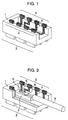
- Fig. 1 is a perspective view showing a package structure of a semiconductor laser module according to the first embodiment
- Fig. 2 is a perspective view showing the construction of the semiconductor laser module formed by assembling a semiconductor device and an optical fiber into the package shown in Fig. 1
- Fig. 3 is a perspective view showing the construction when the semiconductor laser module according to this embodiment is packaged to a printed substrate.
- the semiconductor device accommodation package shown in the drawings comprises a package 1 which is a resin-molded article shaped from a plastic material into a hollow box shape, a conductive circuit pattern 4 formed three-dimensionally by patterning in multiple layers on the surface of this package 1, a silicon substrate 7 bonded and fixed to the bottom of the package 1 and equipped with a V groove (not shown) for installing an optical fiber 6, and a semiconductor device (laser diode) 5 mounted to the silicon substrate 7.
- the optical fiber 6, which is a single mode fiber coupled optically with the laser diode 5, for executing optical transfer, is installed in the V groove described above, and the whole assembly inclusive of this optical fiber 6 is referred to as a "semiconductor laser module".
- a plurality of heat radiation fins 2 are disposed in alignment on one of the end faces of the package 1 (bottom surface of the package; lower side in Fig. 1), and a plurality of protuberances 3 constituting electrode lead terminals connected to a printed substrate 10 for electric connection with the semiconductor device 5 are disposed on the upper surface of the side wall of the package 1 opposing the heat radiation fins 2 (upper surface of the package; upper side in Fig. 1).
- the conductive circuit pattern 4 for electric connection is formed three-dimensionally in multiple layers on, and fitted to, the surface of the package 1 and is connected to each of the electrode lead terminals (protuberances) 3.
- the heat radiation fins 2 and the protuberances 3 of the electrode lead terminals are formed simultaneously and integrally with the package 1 at the time of resin-molding of the package 1 into a unitary structure.
- the mold-resin of the package 1, the heat radiation fins 2 and the protuberances 3 of the electrode lead terminals may be the same material.
- This embodiment uses a material which has high adhesion with the conductive circuit pattern 4 and has by itself a high heat resistance and a high strength, such as a liquid crystal polymer, as the plastic material of the package 1.
- the number of the electrode lead terminals 3 of the package 1 of this embodiment is 8. The liquid crystal polymer used in this embodiment will be explained briefly.
- the liquid crystal polymer is a material having a chemical structure such that its rigid molecules are oriented unidirectionally while keeping a difficultly bendable molecular state even under a molten state and are solidified as-oriented when they are cooled.
- the features of such a material are high elastic modulus, low linear expansion rate, high heat resistance (up to 260°C), etc, and the material is suitable as a plastic material that constitutes the package 1.
- Fig. 2 is a partial sectional perspective view showing the construction of the semiconductor laser module formed by fitting the semiconductor device 5 and the optical fiber 6 into the package 1.
- the semiconductor laser module comprises the laser diode 5 as the semiconductor device, the optical fiber 6 as the single mode fiber for effecting optical transfer, coupled optically with the laser diode 5, the silicon substrate 7 to which the laser diode 5 is mounted and which is equipped with the V groove (not shown) for installing the optical fiber 6 and the plastic-molded package 1 which accommodates these constituent elements, to which the silicon substrate 7 is bonded and fixed, and which is equipped with the heat radiation fins 2 and the protuberances 3 of the electrode lead terminals.
- the silicon substrate 7 is bonded and fixed to the inner bottom surface of the package 1.
- the V groove (not shown) is formed on the upper surface of the silicon substrate 7 by anisotropic etching, and the optical fiber 6 is installed into this V groove by the adhesive 8.
- an electrode wiring (not shown) of conductive circuit pattern is formed by patterning on the upper surface of the silicon substrate 7, and the laser diode 5 is mounted to a predetermined position on this wiring.
- the laser diode 5 is mounted with markers (not shown) formed in advance on the electrode wiring on the upper surface of the silicon substrate 7 as registration marks.
- Wire bonding leads are fitted to the laser diode 5 through the electrode wirings on the upper surface of the silicon substrate 7 so that the laser diode 5 can be electrically connected to the microstrip line 4 as the conductive circuit pattern 4 (partially omitted from the drawings) formed on the surface of the package 1.
- Silicon (Si) is used hereby as the material that constitutes the silicon substrate 7.
- the V groove of the silicon substrate 7 has a predetermined width and depth so that when the optical fiber 6 is installed, the center axis of the optical fiber 6 is in conformity with the laser outgoing axis of the laser diode 5 mounted to the upper surface of the silicon substrate 7.
- the optical coupling portion between the laser diode 5 and the optical fiber 6 is covered with a transparent gel-like resin (not shown) having high laser beam permeability.
- a cover 9 of the optical fiber 6 taken out from the package 1 is fixed to the side wall portion of the package 1 by applying an adhesive 12.
- the package 1 is formed integrally with the heat radiation fins 2 and the protuberances 3 of the electrode lead terminals by molding the plastic material.
- the side wall portion of the package 1 from which the optical fiber 6 is taken out is removed so that the optical fiber 6 can be easily disposed.
- the thickness of the package 1 is 4.5 mm from the distal end of the heat radiation fins 2 to the distal end of the protuberance 3 of the electrode lead terminal, its width is 6.0 mm and its length is 15.0 mm.
- the assembly procedure of the package 1 is as follows. First, the mold resin is poured into a mold heated from 300 to 350°C and a predetermined pressure is applied for one to two minutes. The molded package 1 is then withdrawn from the mold. The package 1 so withdrawn has the heat radiation fins 2 and the protuberances 3 of the electrode lead terminals.
- the pouring inlet of the mold resin is disposed at the edge of the package 1 so that the orientation direction of the molecular chains of the liquid crystal polymer used as the plastic material of the package 1 becomes unidirectional and the molecules are oriented in the direction of the optical axis of the optical fiber 6. It is advisable to set the pouring inlet of the resin to the inner bottom surface of the package on the side where the cover 9 of the optical fiber 6 is taken out or at the corner portion of the heat radiation fins 2, for example.
- the resin pouring inlet may be set to other suitable positions, it may be set so long as the molecules can be oriented in substantially the same direction as the direction of the optical axis of the optical fiber 6 and the set position described above is not particularly limited.
- the elastic modulus can be increased in this direction while the coefficient of linear expansion can be decreased. Accordingly, even when any external force and thermal deformation are applied, the position error of the coupling portion between the laser diode 5 and the optical fiber 6 does not occur so easily and stable optical coupling can be obtained.
- the heat radiation fins 2 and the protuberances 3 of the electrode lead terminals are provided with an inclination of 10 to 15 degrees, for example, so that the package 1 can be easily released from the mold after molding.
- Base plating such as copper plating is applied to the whole surface of the resulting package 1.
- a resist is applied to the copper plating, a circuit pattern depicted in a photomask is transferred to the resist and development is then carried out to expose the copper plating at the circuit portion.
- the microstrip line 4 is formed at a part of the circuit pattern.
- Nickel plating or gold plating and a resin coating to serve as an insulating layer are applied to the circuit portion of the copper plating so exposed, and the resist remaining at portions other than the circuit portion and the copper plating below the resist are removed. In this way, the package 1 having the conductive circuit pattern 4 and the microstrip pattern line 4 equipped with the insulating layer formed three-dimensionally on the surface thereof can be completed.
- the package has a double-shot structure. First, a predetermined conductive circuit pattern 4 and a microstrip line 4 are formed in the package 1 and this package 1 is again molded to form the conductive circuit pattern 4 inside the package 1, too.
- the laser diode 5 is positioned and mounted to the silicon substrate 7 by using the markers (not shown) of the electrode wirings on the surface of the silicon substrate 7 as the registration marks.
- the silicon substrate 7 to which the laser diode 5 is mounted is coupled with the inner bottom surface of the package 1 having the conductive pattern 4 formed thereon.
- the laser diode 5 and the electrode wirings on the upper surface of the silicon substrate 7, and the electrode wirings of the silicon substrate 7 and the conductive circuit pattern 4, are electrically connected by wire bonding leads (not shown), respectively.
- the optical fiber 6 is installed into the V groove of the silicon substrate 7 and is fixed to the V groove by the adhesive 8.
- Laser oscillation is generated by supplying a current to the laser diode 5 so that optical coupling between the laser diode 5 and the optical fiber 6 becomes maximal.
- the optical fiber 6 is positioned at the position at which the optical output from the optical fiber 6 attains the maximum.
- the optical fiber 6 is pushed into the V groove of the silicon substrate 7 and is fixed by the adhesive 8.
- the adhesive 8 is applied in advance into the V groove, and is also applied from above after the optical fiber 6 is fitted into the V groove lest the optical fiber 6 undergoes the positioning error.
- the adhesive 12 is charged to the cover portion 9 of the optical fiber 6 taken out from the side surface of the package 1 and is then left standing inside an oven so as to completely set the respective adhesives 8 and 12.
- a UV-setting resin capable of setting within a short time is hereby used for the adhesives 8 and 12.
- Fig. 3 shows the state where the semiconductor laser modules 13 and 14 are packaged to the printed substrate 10, and driving ICs 11 for driving and controlling the modules are together mounted to the printed substrate 10. Though resistor devices and capacitors are also mounted, they are omitted from the drawing.
- two semiconductor laser modules i.e. a transmission module 13 and a reception module 14, are together mounted as the semiconductor laser modules, to one printed substrate 10.
- the driving Ics 11 are disposed in the proximity of these modules 13 and 14 at electrically optimum positions.
- the modules 13 and 14 are mounted in the surface package type in which the protuberances 3 of the electrode lead terminals are soldered to predetermined positions on the printed substrate 10.
- the adhesive 12 is charged to the cover 9 of the optical fiber 6, for example.
- Two methods are available for soldering; one is a reflow system which collectively solders all the electronic components such as the modules 13 and 14, the driving Ics 11, etc, to the printed substrate 10 and the other post-solders the modules 13 and 14.
- the optical fiber 6 using a coating having high heat resistance is used because the heat resistance of the cover 9 of the optical fiber 6 is low, or a heat-resistant protective tube is fitted to the cover 9 of the optical fiber 6 to prevent the temperature rise.
- a method is preferably employed which executes spot-heating for soldering by laser irradiation or beam irradiation.
- the conductive circuit pattern connected electrically and externally to the laser diode 5 comprises the microstrip line, and this conductive circuit pattern 4 is formed is the package 1 which is resin-molded three-dimensionally. Moreover, the protuberances 3 that constitute the electrode lead terminals and the heat radiation fins 2 are integrally molded with the package 1 at the time of molding of the package 1. Consequently, since this embodiment does not employ the conventional construction which generates the reflection and loss of the electric signals supplied from outside to the laser diode 5, the package according to this embodiment can drive the laser diode 5 at a high speed without the reflection and loss of the electric signals even when the frequency band is high, such as the Mhz to Ghz bands.
- the signal transmission line from the conductive circuit pattern 4 formed on the package 1 comprises the microstrip line, the problems of the wiring length and impedance matching encountered when the laser diode 5 is driven at a high modulation frequency can be solved. Consequently, this embodiment can accomplish the package 1 and the semiconductor laser modules 13 and 14 that can cope with high speed transfer.
- the semiconductor laser modules 13 and 14 can be fitted in the surface package type having high packageability by connecting the protuberances 3 to the printed substrate 10, and even when a plastic material having a low heat transfer rate is used, exothermy at the time of driving of the laser diode 5 can be efficiently radiated by the heat radiation fins. Therefore, a stable optical output can be obtained without the drop of the laser output power and fluctuation of the oscillation wavelength. Because the package 1 is constituted by the plastic molded article and the conductive circuit pattern 4 inclusive of the microstrip line 4 is formed on the surface of the package 1, the components of the package 1 and the components of the conductive circuit portion can be molded integrally and the cost of production can be reduced.
- this embodiment can obtain the semiconductor device accommodation package capable of driving the laser diode 5 at a high speed without causing the reflection and loss of the electric signals, and the semiconductor laser modules 13 and 14 using this package.
- a level difference portion 17 for accommodating and packaging the silicon substrate 7 is defined inside the package 1.
- Like reference numerals will be used in this drawing to identify like constituent elements in the same way as in the first embodiment and the detailed explanation of such members will be omitted.
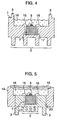
- Fig. 4 shows a longitudinal sectional structure of the semiconductor laser module according to this embodiment.
- the difference of the semiconductor laser module of this embodiment from the semiconductor laser module of the first embodiment is that the level difference portion 17 for accommodating and packaging the silicon substrate 7 inside the package 1 is defined in the trench form at the bottom of the package 1.
- the level difference portion 17 for accommodating and packaging the silicon substrate 1 is formed on the surface opposing the fitting surface of the heat radiation fins 2 of the package 1.
- the silicon substrate 7 is fitted to the bottom of the level difference portion 17, that is, to the bottom of the trench-shaped recess.
- the distance from the fitting surface of the silicon substrate 7 to the heat radiation fins 2 (the thickness of the package 1 at the bottom of the level difference portion 17) is preferably small in order to improve heat radiation efficiency.
- the thickness of the surface of the package 1, on which the heat radiation fins 2 are disposed is preferably small. This thickness is suitably from 0.1 to 0.3 mm. Because the level difference portion 17 is formed in the package 1, the thickness of the package 1 at the position of the level difference portion 17 becomes small, but the package 1 is free from the problem of breakage, etc, due to the drop of the strength because portions other than the level difference portion can be formed to a sufficient thickness.
- the depth of the level difference portion 17 is set to be equal to the height of the silicon substrate 7 so as to reduce the difference of the level between the upper surface of the silicon substrate 7 and that of the level difference portion 17 when the silicon substrate 7 is fitted and to thus reduce the length of the wire bonding leads 15.
- the transparent resin 16 is applied by potting into the package 1, that is, to the optical coupling portion between the laser diode 5 and the optical fiber 6 on the silicon substrate 7, after the silicon substrate 7 and the wire bonding leads 15 are fitted.
- the distance between the silicon substrate 7 and the heat radiation fins 2 can be made smaller than that in the first embodiment. Therefore, heat radiation can be effected efficiently in combination with the electrode lead terminals 3 and the stable optical output can be obtained without causing the drop of the laser output power and fluctuation of the oscillation wavelength.
- the upper surface of the silicon substrate 7 and the upper surface of the level difference portion 17 inside the package 1 are set to the equal level and the length of the wire bonding leads to the conductive circuit pattern 4 inclusive of the microstrip line is reduced. In other words, the problems of the wiring length and impedance matching when the laser diode 5 is high-frequency driven can be solved, the semiconductor laser module that can cope with high frequency transfer can be accomplished.
- this embodiment can obtain the semiconductor device accommodation package capable of driving the laser diode 5 at a high speed without causing the reflection and loss of the electric signals and eventually, the semiconductor laser modules 13 and 14 using this package, can be obtained.
- This embodiment can also obtain the package 1 having a high heat radiation property of the heat generated from the laser diode 5. Since the construction of this embodiment is the same as that of the first embodiment with the exception of the level difference portion 17, it can obtain the same effect as that of the first embodiment.
- a package base 20 equipped with the level difference portion 17 and a package outer frame 19 equipped with side walls extending up beyond the upper surface of the level difference portion 17 and encompassing the outer periphery of the package 20 are molded by double-shot molding in such a manner as to dispose the heat radiation fins 2 and the protuberances 3 of the electrode lead terminals on the surface of the package base 20.
- Like reference numerals will be used in Fig. 5 to identify like constituent elements in the first and second embodiments and the detailed explanation of such members will be omitted.
- Fig. 5 shows a longitudinal section of the semiconductor laser module according to this embodiment.
- the differences of the semiconductor laser module of this embodiment from the semiconductor laser module of the first embodiment reside in that the package 1 is shaped by double-shot molding of the package outer frame 19 and the package base 20, the heat radiation fins 2 and the protuberances 3 of the electrode lead terminals are formed on the same surface of the package base 20 (the surface opposing the printed substrate 10, that is, the surface opposite to the surface having the level difference portion 17), and a cap 18 (a flat sheet member which is fitted to the upper end portion of the side walls and covers a zone defined by the upper surface of the level difference portion 17 of the package base 20 and the inner peripheral surface of the side walls of the package outer frame 19) is provided to the upper surface of the package outer frame 19.
- the level difference portion 17 for accommodating and packaging the silicon substrate 7 is formed in the package base 20.
- the heat radiation fins 2 and the protuberances 3 of the electrode lead terminals are formed by integral molding with the package base 20 equipped with the level difference portion 17.
- This package base 20 is again molded to form the package outer frame 19.
- the transparent resin 16 is charged by potting into the zone defined by the package outer frame 19, the package base 20 and the cap 18 so as to establish a simple hermetic zone in cooperation with the cap 18.
- the combination of a plastic material which is easy to mold the conductive circuit pattern 4 inclusive of the microstrip line and has high heat resistance and high strength with a plastic material capable of re-molding is suitably used for the plastic materials that constitute the package base 20 and the package base 20 and the package outer frame 19.
- This embodiment uses the liquid crystal polymer, for example, as the plastic material that constitutes both the package outer frame 19 and the package base 20, and property values suitable for the intended application are selected.
- the package outer frame 19 and the package base 20 are molded by double-shot molding. Therefore, the conductive circuit pattern 4 inclusive of the microstrip line can be formed not only on the surface of the package outer frame 19 that serves as the surface after completion of the package and on the surface of the package 20 but also at the portions which become the interior of the packager after its completion (the coupling surface between the package outer frame 19 and the package base 20), so that design of the electric wirings can be made optimally. Further, because the protuberances 3 of the electrode lead terminals can be disposed at arbitrary positions, the package outer frame 19 and the package base 20 suitable for high speed transfer can be obtained.
- packaging to the printed substrate 10 is not effected by the protuberances 3 of the electrode lead terminals alone but the heat radiation fins 2, too, are fitted to the printed substrate 10, heat radiation can be attained more efficiently and the semiconductor laser diode having the stable optical output can be obtained without causing the drop of the laser output power and fluctuation of the oscillation wavelength. Further, service life of the semiconductor laser diode can be extended by employing the simple hermetic structure. Because this embodiment employs the same construction as those of the first and second embodiments with the exception of double-shot molding and the cap 18, it can obtain the same effects as those of the first and second embodiments.
- the package 1 is shaped by double-shot molding of the package base 22 equipped with the level difference portion 17 and the package outer frame 21 coupled with the upper surface of the package base 22 and defining the side walls, the protuberances 3 of the electrode lead terminals are disposed on the side surfaces of the package base 22 and the heat radiation fins 2 are disposed on the bottom surface of the package base 22.
- the protuberances 3 of the electrode lead terminals are disposed on the side surfaces of the package base 22 and the heat radiation fins 2 are disposed on the bottom surface of the package base 22.
- Like reference numerals will be used in these drawings to identify like constituent elements as in the first to third embodiments, and the explanation of such members will be omitted.
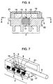
- Fig. 6 shows a longitudinal sectional structure of the semiconductor laser module according to this embodiment
- Fig. 7 is a partial sectional perspective view.
- the semiconductor laser module of this embodiment from the semiconductor laser module of the first embodiment are that the package 1 is formed by double-shot molding of the package outer frame 21 and the package base 22, the protuberances 3 of the electrode lead terminal are disposed on the side surfaces of the package base 22, the heat radiation fins 2 are disposed on the bottom surface of the package base 22 and the cap 18 (a flat sheet member fitted to the upper end portion of the side walls and covering the zone defined by the upper surface of the level difference portion 17 of the package base 22 and the inner peripheral surface of the side walls of the package outer frame 21) is provided to the upper surface of the package outer frame 21.
- the level difference portion 17 for accommodating and packaging the silicon substrate 7 is formed in the package base 22.
- the package base 22 having the level difference portion 17 includes the heat radiation fins 2 and the protuberances 3 of the electrode lead terminals that are molded integrally with the package base 22.
- the conductive circuit pattern 4 and the microstrip line 24 for electrically connecting the laser diode 5 and the electrode lead terminals 3 are formed on the surface of the package base 22.
- This package base 22 is again molded to form the package outer frame 21 as the framework of the package.
- the transparent resin 16 is charged by potting into the zone defined by the upper surface of the level difference portion 17 of the package base 22 and the inner peripheral surface of the side walls of the package outer frame 21 and the cap 18 is further fitted so as to establish the simple hermetic structure inside the zone.
- this embodiment uses the liquid crystal polymer, for example, as the plastic material of both of the package outer frame 21 and the package base 22, and property values suitable for the intended application are selected.
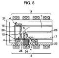
- Fig. 8 is a top view showing the wiring structure of the conductive circuit pattern 4 and the microstrip line 24 formed on the package base 22.
- a photodiode 26 is fitted to the upper surface of the silicon substrate 7 of the semiconductor laser module shown in Figs. 6 and 7 adjacent to the laser diode 5.
- the optical fiber 6 and the adhesive 8 are omitted from the drawing.
- the protuberances 3 of the electrode lead terminals electrically connected to the laser diode 5 and the photodiode 26 are disposed at two to four positions.
- the laser diode 5 and the photodiode 26 are electrically connected to the conductive circuit pattern 4 on the silicon substrate 7 through the wire bonding leads 15 while the conductive circuit pattern 4 on the silicon substrate 7 is electrically connected to the conductive circuit pattern 4 and the microstrip line 24 formed on the package base 22 through the wire bonding leads 15.
- the conductive circuit pattern on the surface of the package base 22 to be electrically connected to the laser diode 5 comprises the microstrip line 24 and is connected to the conductive circuit pattern 4 on the silicon substrate 7 through ribbon-like wirings 25.
- the microstrip line 24 has a multi-layered wiring structure equipped with insulating layers.
- the silicon substrate 7 is equipped with the V groove 17 for installing the optical fiber 7.
- the conductive circuit pattern 4 and the microstrip line 14 formed on the package 22 have only a two-dimensional planar shape and three-dimensional bending occurs only around the protuberances 3 that constitute the electrode lead terminals.
- the two-dimensional planar shape can reduce bending of the signal transfer lines, and the reflection and loss of the electric signals supplied from outside to the laser diode 5 can be further reduced, and the laser diode 5 can be driven at a high speed even when a modulation frequency is high such as in the MHz to GHz bands.
- the structure of the package outer frame 21 and the package base 22, and the semiconductor laser module suitable for high speed transfer can be accomplished. Because this embodiment employs the same construction as those of the first to third embodiments, it can obtain the same effect as those of the first to third embodiments.
- the first to fourth embodiment represent the semiconductor laser module using the laser diode 5 as the semiconductor device
- a package suitable for high speed transfer can be accomplished by forming the semiconductor light reception module by mounting the photodiode in place of the laser diode 5 and in such a case, too, the same effect as those of the foregoing embodiments can be obtained.
- the first to fourth embodiments represent the construction in which the laser diode 5 and the optical fiber 6 and the silicon substrate 7 having these elements mounted thereto are accommodated and packaged to the package 1, but the present invention is not particularly limited to these members.
- the package of the present invention is not limited to these members and can be accomplished by the construction which together accommodates and packages the driving ICs 11 for driving and controlling the semiconductor devices.
- the number of the protuberances 3 of the electrode lead terminals increases because the number of electric connections with outside increases.
- the conductive circuit pattern 4 and the microstrip line 4 can be formed in an arbitrary shape by single-shot or double-shot molding of the plastic material, the number of the protuberances 3 of the electrode terminals can be increased or decreased easily and the positions of their disposition can be changed easily by a simple modification, and the construction can be constituted so as to cope with various shapes of the package 1.
- the first to fourth embodiments described above use the liquid crystal polymer for the plastic material constituting the package 1 but the present invention is not particularly limited thereto. Therefore, other plastic materials can be used for the package 1 of the semiconductor laser module capable of positioning in the order of sub-micron order such as in optical coupling between the laser diode 5 and the optical fiber 6 and fixing them semi-permanently so long as they have a high elastic modulus, a low thermal expansion coefficient, a high heat resistance (capable of withstanding solder reflow), etc. It is possible to use, for example, a composite material of heat setting type plastics prepared by mixing glass fibers, carbon fibers, glass fillers, and so forth.
Landscapes
- Physics & Mathematics (AREA)
- General Physics & Mathematics (AREA)
- Optics & Photonics (AREA)
- Semiconductor Lasers (AREA)
- Optical Couplings Of Light Guides (AREA)
Applications Claiming Priority (2)
| Application Number | Priority Date | Filing Date | Title |
|---|---|---|---|
| JP34035997A JP3543189B2 (ja) | 1997-12-10 | 1997-12-10 | 半導体素子パッケージおよび半導体装置 |
| JP34035997 | 1997-12-10 |
Publications (2)
| Publication Number | Publication Date |
|---|---|
| EP0928026A1 true EP0928026A1 (fr) | 1999-07-07 |
| EP0928026B1 EP0928026B1 (fr) | 2003-07-23 |
Family
ID=18336193
Family Applications (1)
| Application Number | Title | Priority Date | Filing Date |
|---|---|---|---|
| EP98123179A Expired - Lifetime EP0928026B1 (fr) | 1997-12-10 | 1998-12-04 | Boítier moulé en plastique pour un dispositif semi-conducteur |
Country Status (3)
| Country | Link |
|---|---|
| EP (1) | EP0928026B1 (fr) |
| JP (1) | JP3543189B2 (fr) |
| DE (1) | DE69816581T2 (fr) |
Cited By (6)
| Publication number | Priority date | Publication date | Assignee | Title |
|---|---|---|---|---|
| EP1118893A3 (fr) * | 2000-01-18 | 2004-01-28 | Nippon Telegraph and Telephone Corporation | Module optique utilisant des conducteurs intégrés dans un substrat de résine |
| EP1227349A3 (fr) * | 2001-01-18 | 2004-06-23 | Autonetworks Technologies, Ltd. | Connecteur optique et connecteur blindé |
| WO2005039259A1 (fr) * | 2003-10-13 | 2005-04-28 | Fraunhofer-Gesellschaft zur Förderung der angewandten Forschung e.V. | Substrats ceramiques a structures mecaniques integrees pour le montage direct de composants optiques |
| US7002803B2 (en) | 2002-02-27 | 2006-02-21 | Nec Compound Semiconductor Devices, Ltd. | Electronic product with heat radiating plate |
| US10433428B2 (en) | 2015-06-29 | 2019-10-01 | Molex, Llc | Application specific electronics packaging systems, methods and devices |
| US11244875B2 (en) | 2018-12-06 | 2022-02-08 | Mitsubishi Electric Corporation | Semiconductor device and manufacturing method for semiconductor device |
Families Citing this family (5)
| Publication number | Priority date | Publication date | Assignee | Title |
|---|---|---|---|---|
| JP5669494B2 (ja) * | 2010-09-16 | 2015-02-12 | 京セラ株式会社 | 素子収納用パッケージ、およびこれを備えた電子装置 |
| JP7013879B2 (ja) * | 2018-01-12 | 2022-02-01 | 住友大阪セメント株式会社 | 光変調器、及びそれを用いた光送信装置 |
| JP7013880B2 (ja) * | 2018-01-12 | 2022-02-01 | 住友大阪セメント株式会社 | 光変調器、及び光送信装置 |
| JP6910976B2 (ja) * | 2018-02-16 | 2021-07-28 | 京セラ株式会社 | 光モジュール |
| JP7013942B2 (ja) * | 2018-02-28 | 2022-02-01 | 住友大阪セメント株式会社 | 光変調器、及び光伝送装置 |
Citations (6)
| Publication number | Priority date | Publication date | Assignee | Title |
|---|---|---|---|---|
| JPS59229840A (ja) * | 1983-05-30 | 1984-12-24 | Rohm Co Ltd | 半導体装置 |
| US5200367A (en) * | 1990-11-13 | 1993-04-06 | Gold Star Electron Co., Ltd. | Method for assembling packages of semi-conductor elements |
| EP0578411A1 (fr) * | 1992-07-06 | 1994-01-12 | Advanced Micro Devices, Inc. | Refroidisseurs pour des empaquetages de circuits intégrés |
| US5483740A (en) * | 1994-05-26 | 1996-01-16 | Ak Technology, Inc. | Method of making homogeneous thermoplastic semi-conductor chip carrier package |
| JPH0818163A (ja) * | 1994-06-24 | 1996-01-19 | Nippon Telegr & Teleph Corp <Ntt> | 光装置 |
| WO1997015077A1 (fr) * | 1995-10-16 | 1997-04-24 | Siemens N.V. | Boitier de matrice a bossage polymere pour circuits a micro-ondes |
-
1997
- 1997-12-10 JP JP34035997A patent/JP3543189B2/ja not_active Expired - Lifetime
-
1998
- 1998-12-04 DE DE69816581T patent/DE69816581T2/de not_active Expired - Lifetime
- 1998-12-04 EP EP98123179A patent/EP0928026B1/fr not_active Expired - Lifetime
Patent Citations (6)
| Publication number | Priority date | Publication date | Assignee | Title |
|---|---|---|---|---|
| JPS59229840A (ja) * | 1983-05-30 | 1984-12-24 | Rohm Co Ltd | 半導体装置 |
| US5200367A (en) * | 1990-11-13 | 1993-04-06 | Gold Star Electron Co., Ltd. | Method for assembling packages of semi-conductor elements |
| EP0578411A1 (fr) * | 1992-07-06 | 1994-01-12 | Advanced Micro Devices, Inc. | Refroidisseurs pour des empaquetages de circuits intégrés |
| US5483740A (en) * | 1994-05-26 | 1996-01-16 | Ak Technology, Inc. | Method of making homogeneous thermoplastic semi-conductor chip carrier package |
| JPH0818163A (ja) * | 1994-06-24 | 1996-01-19 | Nippon Telegr & Teleph Corp <Ntt> | 光装置 |
| WO1997015077A1 (fr) * | 1995-10-16 | 1997-04-24 | Siemens N.V. | Boitier de matrice a bossage polymere pour circuits a micro-ondes |
Non-Patent Citations (2)
| Title |
|---|
| PATENT ABSTRACTS OF JAPAN vol. 009, no. 102 (E - 312) 4 May 1985 (1985-05-04) * |
| PATENT ABSTRACTS OF JAPAN vol. 096, no. 005 31 May 1996 (1996-05-31) * |
Cited By (10)
| Publication number | Priority date | Publication date | Assignee | Title |
|---|---|---|---|---|
| EP1118893A3 (fr) * | 2000-01-18 | 2004-01-28 | Nippon Telegraph and Telephone Corporation | Module optique utilisant des conducteurs intégrés dans un substrat de résine |
| EP1227349A3 (fr) * | 2001-01-18 | 2004-06-23 | Autonetworks Technologies, Ltd. | Connecteur optique et connecteur blindé |
| US7002803B2 (en) | 2002-02-27 | 2006-02-21 | Nec Compound Semiconductor Devices, Ltd. | Electronic product with heat radiating plate |
| WO2005039259A1 (fr) * | 2003-10-13 | 2005-04-28 | Fraunhofer-Gesellschaft zur Förderung der angewandten Forschung e.V. | Substrats ceramiques a structures mecaniques integrees pour le montage direct de composants optiques |
| US10433428B2 (en) | 2015-06-29 | 2019-10-01 | Molex, Llc | Application specific electronics packaging systems, methods and devices |
| US10667407B2 (en) | 2015-06-29 | 2020-05-26 | Molex, Llc | Application specific electronics packaging systems, methods and devices |
| US10905014B2 (en) | 2015-06-29 | 2021-01-26 | Molex, Llc | Application specific electronics packaging systems, methods and devices |
| US11503718B2 (en) | 2015-06-29 | 2022-11-15 | Molex, Llc | Application specific electronics packaging systems, methods and devices |
| US11244875B2 (en) | 2018-12-06 | 2022-02-08 | Mitsubishi Electric Corporation | Semiconductor device and manufacturing method for semiconductor device |
| US11676871B2 (en) | 2018-12-06 | 2023-06-13 | Mitsubishi Electric Corporation | Semiconductor device and manufacturing method for semiconductor device |
Also Published As
| Publication number | Publication date |
|---|---|
| DE69816581T2 (de) | 2004-06-03 |
| JPH11176966A (ja) | 1999-07-02 |
| EP0928026B1 (fr) | 2003-07-23 |
| JP3543189B2 (ja) | 2004-07-14 |
| DE69816581D1 (de) | 2003-08-28 |
Similar Documents
| Publication | Publication Date | Title |
|---|---|---|
| US6467972B2 (en) | Optical interconnection module | |
| US10270532B2 (en) | Optical transmission module | |
| US8168453B2 (en) | Light emitting diode package and fabrication method thereof | |
| US6632027B1 (en) | Optical module | |
| US6995510B2 (en) | Light-emitting unit and method for producing same as well as lead frame used for producing light-emitting unit | |
| US7875901B2 (en) | Optical device package and optical semiconductor device using the same | |
| US7048450B2 (en) | Optoelectronic module with transmitter chip and connecting piece for the module with respect to an optical fiber and with respect to a circuit board, and methods for producing the same | |
| US7086788B2 (en) | Optical sub-assembly for opto-electronic modules | |
| US7050678B1 (en) | Optical module, optical element attachment method, and receptacle-fitted optical module | |
| JP3684305B2 (ja) | 半導体レーザ結合装置および半導体受光装置 | |
| EP0928026B1 (fr) | Boítier moulé en plastique pour un dispositif semi-conducteur | |
| JP2004354532A (ja) | 光モジュール及びその製造方法、光通信装置、電子機器 | |
| EP0331436A2 (fr) | Appareil pour communication optique | |
| TW201909436A (zh) | 光模組 | |
| WO2002014917A1 (fr) | Plaque de montage optique, module optique, emetteur/recepteur optique, systeme emetteur/recepteur optique et procede de fabrication de plaque de montage optique | |
| JP2004271648A (ja) | 光通信モジュール、光通信装置、及びその製造方法 | |
| US7171066B1 (en) | Optical module and optical transmission device | |
| KR100372034B1 (ko) | 송신기 모듈 및 수신기 모듈의 캡슐화 장치 | |
| US20060239621A1 (en) | Optical module and method for manufacturing same | |
| US7101092B2 (en) | Module having a circuit carrier and an electro-optical transducer and method for producing the same | |
| US20250093599A1 (en) | Optical module assembly | |
| JP2006120781A (ja) | 光電変換モジュール | |
| JP2002296464A (ja) | 光電気配線基板 | |
| WO2003098304A1 (fr) | Module optique de type enfichable | |
| JP2007035697A (ja) | 光電気変換モジュール |
Legal Events
| Date | Code | Title | Description |
|---|---|---|---|
| PUAI | Public reference made under article 153(3) epc to a published international application that has entered the european phase |
Free format text: ORIGINAL CODE: 0009012 |
|
| AK | Designated contracting states |
Kind code of ref document: A1 Designated state(s): DE FR GB |
|
| AX | Request for extension of the european patent |
Free format text: AL;LT;LV;MK;RO;SI |
|
| 17P | Request for examination filed |
Effective date: 19990726 |
|
| AKX | Designation fees paid |
Free format text: DE FR GB |
|
| 17Q | First examination report despatched |
Effective date: 20000731 |
|
| GRAH | Despatch of communication of intention to grant a patent |
Free format text: ORIGINAL CODE: EPIDOS IGRA |
|
| GRAH | Despatch of communication of intention to grant a patent |
Free format text: ORIGINAL CODE: EPIDOS IGRA |
|
| GRAA | (expected) grant |
Free format text: ORIGINAL CODE: 0009210 |
|
| AK | Designated contracting states |
Designated state(s): DE FR GB |
|
| REG | Reference to a national code |
Ref country code: GB Ref legal event code: FG4D |
|
| REF | Corresponds to: |
Ref document number: 69816581 Country of ref document: DE Date of ref document: 20030828 Kind code of ref document: P |
|
| ET | Fr: translation filed | ||
| PLBE | No opposition filed within time limit |
Free format text: ORIGINAL CODE: 0009261 |
|
| STAA | Information on the status of an ep patent application or granted ep patent |
Free format text: STATUS: NO OPPOSITION FILED WITHIN TIME LIMIT |
|
| 26N | No opposition filed |
Effective date: 20040426 |
|
| REG | Reference to a national code |
Ref country code: GB Ref legal event code: 732E Free format text: REGISTERED BETWEEN 20121018 AND 20121024 |
|
| REG | Reference to a national code |
Ref country code: DE Ref legal event code: R082 Ref document number: 69816581 Country of ref document: DE Representative=s name: STREHL, SCHUEBEL-HOPF & PARTNER, DE |
|
| REG | Reference to a national code |
Ref country code: FR Ref legal event code: TP Owner name: OPNEXT JAPAN, INC., JP Effective date: 20121022 |
|
| REG | Reference to a national code |
Ref country code: DE Ref legal event code: R082 Ref document number: 69816581 Country of ref document: DE Representative=s name: PATENTANWAELTE STREHL, SCHUEBEL-HOPF & PARTNER, DE Effective date: 20121116 Ref country code: DE Ref legal event code: R082 Ref document number: 69816581 Country of ref document: DE Representative=s name: STREHL, SCHUEBEL-HOPF & PARTNER, DE Effective date: 20121116 Ref country code: DE Ref legal event code: R081 Ref document number: 69816581 Country of ref document: DE Owner name: OPNEXT JAPAN,INC., YOKOHAMA, JP Free format text: FORMER OWNER: HITACHI, LTD., TOKYO, JP Effective date: 20121116 Ref country code: DE Ref legal event code: R081 Ref document number: 69816581 Country of ref document: DE Owner name: OPNEXT JAPAN,INC., JP Free format text: FORMER OWNER: HITACHI, LTD., TOKYO, JP Effective date: 20121116 |
|
| PGFP | Annual fee paid to national office [announced via postgrant information from national office to epo] |
Ref country code: GB Payment date: 20131204 Year of fee payment: 16 Ref country code: DE Payment date: 20131127 Year of fee payment: 16 |
|
| PGFP | Annual fee paid to national office [announced via postgrant information from national office to epo] |
Ref country code: FR Payment date: 20131209 Year of fee payment: 16 |
|
| REG | Reference to a national code |
Ref country code: DE Ref legal event code: R119 Ref document number: 69816581 Country of ref document: DE |
|
| GBPC | Gb: european patent ceased through non-payment of renewal fee |
Effective date: 20141204 |
|
| REG | Reference to a national code |
Ref country code: FR Ref legal event code: ST Effective date: 20150831 |
|
| PG25 | Lapsed in a contracting state [announced via postgrant information from national office to epo] |
Ref country code: GB Free format text: LAPSE BECAUSE OF NON-PAYMENT OF DUE FEES Effective date: 20141204 Ref country code: DE Free format text: LAPSE BECAUSE OF NON-PAYMENT OF DUE FEES Effective date: 20150701 |
|
| PG25 | Lapsed in a contracting state [announced via postgrant information from national office to epo] |
Ref country code: FR Free format text: LAPSE BECAUSE OF NON-PAYMENT OF DUE FEES Effective date: 20141231 |