EP0928059A2 - Current-voltage converter and relative control circuit - Google Patents
Current-voltage converter and relative control circuit Download PDFInfo
- Publication number
- EP0928059A2 EP0928059A2 EP99100017A EP99100017A EP0928059A2 EP 0928059 A2 EP0928059 A2 EP 0928059A2 EP 99100017 A EP99100017 A EP 99100017A EP 99100017 A EP99100017 A EP 99100017A EP 0928059 A2 EP0928059 A2 EP 0928059A2
- Authority
- EP
- European Patent Office
- Prior art keywords
- current
- voltage
- output
- circuit
- input
- Prior art date
- Legal status (The legal status is an assumption and is not a legal conclusion. Google has not performed a legal analysis and makes no representation as to the accuracy of the status listed.)
- Granted
Links
Images


Classifications
-
- H—ELECTRICITY
- H02—GENERATION; CONVERSION OR DISTRIBUTION OF ELECTRIC POWER
- H02M—APPARATUS FOR CONVERSION BETWEEN AC AND AC, BETWEEN AC AND DC, OR BETWEEN DC AND DC, AND FOR USE WITH MAINS OR SIMILAR POWER SUPPLY SYSTEMS; CONVERSION OF DC OR AC INPUT POWER INTO SURGE OUTPUT POWER; CONTROL OR REGULATION THEREOF
- H02M1/00—Details of apparatus for conversion
- H02M1/42—Circuits or arrangements for compensating for or adjusting power factor in converters or inverters
- H02M1/4208—Arrangements for improving power factor of AC input
- H02M1/4258—Arrangements for improving power factor of AC input using a single converter stage both for correction of AC input power factor and generation of a regulated and galvanically isolated DC output voltage
-
- H—ELECTRICITY
- H02—GENERATION; CONVERSION OR DISTRIBUTION OF ELECTRIC POWER
- H02M—APPARATUS FOR CONVERSION BETWEEN AC AND AC, BETWEEN AC AND DC, OR BETWEEN DC AND DC, AND FOR USE WITH MAINS OR SIMILAR POWER SUPPLY SYSTEMS; CONVERSION OF DC OR AC INPUT POWER INTO SURGE OUTPUT POWER; CONTROL OR REGULATION THEREOF
- H02M3/00—Conversion of DC power input into DC power output
- H02M3/22—Conversion of DC power input into DC power output with intermediate conversion into AC
- H02M3/24—Conversion of DC power input into DC power output with intermediate conversion into AC by static converters
- H02M3/28—Conversion of DC power input into DC power output with intermediate conversion into AC by static converters using discharge tubes with control electrode or semiconductor devices with control electrode to produce the intermediate AC
- H02M3/285—Single converters with a plurality of output stages connected in parallel
-
- H—ELECTRICITY
- H02—GENERATION; CONVERSION OR DISTRIBUTION OF ELECTRIC POWER
- H02M—APPARATUS FOR CONVERSION BETWEEN AC AND AC, BETWEEN AC AND DC, OR BETWEEN DC AND DC, AND FOR USE WITH MAINS OR SIMILAR POWER SUPPLY SYSTEMS; CONVERSION OF DC OR AC INPUT POWER INTO SURGE OUTPUT POWER; CONTROL OR REGULATION THEREOF
- H02M3/00—Conversion of DC power input into DC power output
- H02M3/22—Conversion of DC power input into DC power output with intermediate conversion into AC
- H02M3/24—Conversion of DC power input into DC power output with intermediate conversion into AC by static converters
- H02M3/28—Conversion of DC power input into DC power output with intermediate conversion into AC by static converters using discharge tubes with control electrode or semiconductor devices with control electrode to produce the intermediate AC
- H02M3/325—Conversion of DC power input into DC power output with intermediate conversion into AC by static converters using discharge tubes with control electrode or semiconductor devices with control electrode to produce the intermediate AC using devices of a triode or a transistor type requiring continuous application of a control signal
- H02M3/335—Conversion of DC power input into DC power output with intermediate conversion into AC by static converters using discharge tubes with control electrode or semiconductor devices with control electrode to produce the intermediate AC using devices of a triode or a transistor type requiring continuous application of a control signal using semiconductor devices only
-
- H—ELECTRICITY
- H02—GENERATION; CONVERSION OR DISTRIBUTION OF ELECTRIC POWER
- H02M—APPARATUS FOR CONVERSION BETWEEN AC AND AC, BETWEEN AC AND DC, OR BETWEEN DC AND DC, AND FOR USE WITH MAINS OR SIMILAR POWER SUPPLY SYSTEMS; CONVERSION OF DC OR AC INPUT POWER INTO SURGE OUTPUT POWER; CONTROL OR REGULATION THEREOF
- H02M3/00—Conversion of DC power input into DC power output
- H02M3/22—Conversion of DC power input into DC power output with intermediate conversion into AC
- H02M3/24—Conversion of DC power input into DC power output with intermediate conversion into AC by static converters
- H02M3/28—Conversion of DC power input into DC power output with intermediate conversion into AC by static converters using discharge tubes with control electrode or semiconductor devices with control electrode to produce the intermediate AC
- H02M3/325—Conversion of DC power input into DC power output with intermediate conversion into AC by static converters using discharge tubes with control electrode or semiconductor devices with control electrode to produce the intermediate AC using devices of a triode or a transistor type requiring continuous application of a control signal
- H02M3/335—Conversion of DC power input into DC power output with intermediate conversion into AC by static converters using discharge tubes with control electrode or semiconductor devices with control electrode to produce the intermediate AC using devices of a triode or a transistor type requiring continuous application of a control signal using semiconductor devices only
- H02M3/33561—Conversion of DC power input into DC power output with intermediate conversion into AC by static converters using discharge tubes with control electrode or semiconductor devices with control electrode to produce the intermediate AC using devices of a triode or a transistor type requiring continuous application of a control signal using semiconductor devices only having more than one ouput with independent control
-
- H—ELECTRICITY
- H02—GENERATION; CONVERSION OR DISTRIBUTION OF ELECTRIC POWER
- H02M—APPARATUS FOR CONVERSION BETWEEN AC AND AC, BETWEEN AC AND DC, OR BETWEEN DC AND DC, AND FOR USE WITH MAINS OR SIMILAR POWER SUPPLY SYSTEMS; CONVERSION OF DC OR AC INPUT POWER INTO SURGE OUTPUT POWER; CONTROL OR REGULATION THEREOF
- H02M3/00—Conversion of DC power input into DC power output
- H02M3/22—Conversion of DC power input into DC power output with intermediate conversion into AC
- H02M3/24—Conversion of DC power input into DC power output with intermediate conversion into AC by static converters
- H02M3/28—Conversion of DC power input into DC power output with intermediate conversion into AC by static converters using discharge tubes with control electrode or semiconductor devices with control electrode to produce the intermediate AC
- H02M3/325—Conversion of DC power input into DC power output with intermediate conversion into AC by static converters using discharge tubes with control electrode or semiconductor devices with control electrode to produce the intermediate AC using devices of a triode or a transistor type requiring continuous application of a control signal
- H02M3/335—Conversion of DC power input into DC power output with intermediate conversion into AC by static converters using discharge tubes with control electrode or semiconductor devices with control electrode to produce the intermediate AC using devices of a triode or a transistor type requiring continuous application of a control signal using semiconductor devices only
- H02M3/33569—Conversion of DC power input into DC power output with intermediate conversion into AC by static converters using discharge tubes with control electrode or semiconductor devices with control electrode to produce the intermediate AC using devices of a triode or a transistor type requiring continuous application of a control signal using semiconductor devices only having several active switching elements
-
- H—ELECTRICITY
- H02—GENERATION; CONVERSION OR DISTRIBUTION OF ELECTRIC POWER
- H02M—APPARATUS FOR CONVERSION BETWEEN AC AND AC, BETWEEN AC AND DC, OR BETWEEN DC AND DC, AND FOR USE WITH MAINS OR SIMILAR POWER SUPPLY SYSTEMS; CONVERSION OF DC OR AC INPUT POWER INTO SURGE OUTPUT POWER; CONTROL OR REGULATION THEREOF
- H02M7/00—Conversion of AC power input into DC power output; Conversion of DC power input into AC power output
- H02M7/42—Conversion of DC power input into AC power output without possibility of reversal
- H02M7/44—Conversion of DC power input into AC power output without possibility of reversal by static converters
- H02M7/48—Conversion of DC power input into AC power output without possibility of reversal by static converters using discharge tubes with control electrode or semiconductor devices with control electrode
- H02M7/493—Conversion of DC power input into AC power output without possibility of reversal by static converters using discharge tubes with control electrode or semiconductor devices with control electrode the static converters being arranged for operation in parallel
-
- H—ELECTRICITY
- H02—GENERATION; CONVERSION OR DISTRIBUTION OF ELECTRIC POWER
- H02M—APPARATUS FOR CONVERSION BETWEEN AC AND AC, BETWEEN AC AND DC, OR BETWEEN DC AND DC, AND FOR USE WITH MAINS OR SIMILAR POWER SUPPLY SYSTEMS; CONVERSION OF DC OR AC INPUT POWER INTO SURGE OUTPUT POWER; CONTROL OR REGULATION THEREOF
- H02M1/00—Details of apparatus for conversion
- H02M1/0067—Converter structures employing plural converter units, other than for parallel operation of the units on a single load
- H02M1/0074—Plural converter units whose inputs are connected in series
-
- H—ELECTRICITY
- H02—GENERATION; CONVERSION OR DISTRIBUTION OF ELECTRIC POWER
- H02M—APPARATUS FOR CONVERSION BETWEEN AC AND AC, BETWEEN AC AND DC, OR BETWEEN DC AND DC, AND FOR USE WITH MAINS OR SIMILAR POWER SUPPLY SYSTEMS; CONVERSION OF DC OR AC INPUT POWER INTO SURGE OUTPUT POWER; CONTROL OR REGULATION THEREOF
- H02M1/00—Details of apparatus for conversion
- H02M1/0083—Converters characterised by their input or output configuration
- H02M1/009—Converters characterised by their input or output configuration having two or more independently controlled outputs
-
- Y—GENERAL TAGGING OF NEW TECHNOLOGICAL DEVELOPMENTS; GENERAL TAGGING OF CROSS-SECTIONAL TECHNOLOGIES SPANNING OVER SEVERAL SECTIONS OF THE IPC; TECHNICAL SUBJECTS COVERED BY FORMER USPC CROSS-REFERENCE ART COLLECTIONS [XRACs] AND DIGESTS
- Y02—TECHNOLOGIES OR APPLICATIONS FOR MITIGATION OR ADAPTATION AGAINST CLIMATE CHANGE
- Y02B—CLIMATE CHANGE MITIGATION TECHNOLOGIES RELATED TO BUILDINGS, e.g. HOUSING, HOUSE APPLIANCES OR RELATED END-USER APPLICATIONS
- Y02B70/00—Technologies for an efficient end-user side electric power management and consumption
- Y02B70/10—Technologies improving the efficiency by using switched-mode power supplies [SMPS], i.e. efficient power electronics conversion e.g. power factor correction or reduction of losses in power supplies or efficient standby modes
Definitions
- the invention relates on the one hand to a current-voltage converter, in particular for high input voltages, including a primary side that has several in series Subsystems with at least one transistor circuit breaker and one each has its own assigned transformer primary winding and a secondary side which the subsystems are coupled to a common load output and on the other hand to a current-voltage converter, in particular for high input currents, comprising a Primary side, which has several subsystems connected in parallel, each with at least one Transistor circuit breakers and their own assigned transformer primary winding has, and a secondary side, via which the subsystems to a common Load output are coupled and to an associated control loop, including a Voltage regulator with voltage comparator and voltage amplifier as well as a current regulator with current comparator and current amplifier as well as between voltage regulator and current regulator arranged correction element.
- double booster topologies which have an intermediate circuit have an electrolyte code, so that this or the upstream network Applying the high input voltage due to the penetration without short-circuit current limitation is charged. Therefore, this capacitor must be at the peak voltage at the input be designed, which is higher than the regulated output voltage of the booster.
- the used components problems. So the semiconductors used must be like transistors and diodes can be adapted to the maximum input voltage or current and the The transformers used must match both the power and voltage Processing input voltage are adjusted, whereby unacceptable winding and Winding voltages occur.
- the primary side is made up of several subsystems connected in series, which each contain a transistor circuit breaker arrangement, each of which has its own Transformer primary winding is assigned, which is on the secondary side of the converter are coupled to a common load output.
- the coupling causes the Transformer winding voltage an automatic, dynamic and quasi lossless Voltage symmetry between the subsystems in load operation.
- the transformer windings are "hard" parallel on the secondary side switched. This has the disadvantage that asymmetries with non-current-limited ones lead dynamic balancing currents, but which only bring about the symmetrization.
- This circuit arrangement also has the disadvantage that with converters AC voltage input a connection of the peak value of the rectified voltage to a very large capacitor directly at the output of a rectifier Capacitance occurs and all of these forward converter topologies have none of the input voltage waveform Allow adjusted current consumption (Power Factor Correction PFC).
- the present invention is therefore based on the problem of a converter for high To provide input voltages or currents of simple construction has and the voltage or current symmetry is improved.
- the problem is solved according to the invention in the case of a converter, in particular for high input voltages solved in that the subsystems connected in series each have a branch have inductance on the input side and the at least one transistor power switch, the inductances at least temporarily via the respective transistor power switches electrically in series at the input voltage and a voltage symmetry between cause the subsystems and where an output of the subsystems with each Transformer primary winding is connected as an isolating transformer for power supply.
- the problem is solved according to the invention in that the subsystems connected in parallel each have a branch with an inductor on the input side and the at least one transistor circuit breaker, which at least at times at times electrically parallel to the input voltage via the respective transistor circuit breaker U E lies and causes a current symmetry between the subsystems and that in each case one output of the subsystems is connected to each of the transformer primary winding as an isolating transformer for power supply.
- this topology causes a power supply in the transformer. This means that each primary winding has its current in the flow concept transfers and thus impresses on the secondary burden.
- each subsystem By synchronously triggering all transistor circuit breakers arranged in the subsystems, each subsystem works with a subvoltage or a subcurrent which results from the input voltage U E or input current I E divided by the number N of subsystems connected in series or in parallel .
- commercially available components that do not have to meet high-voltage requirements can be used both for the design of the transistor circuit breakers and for the design of the inductances such as inductors and isolating transformers. This significantly reduces costs.
- the essential difference from the circuit structure according to the prior art is that the current / voltage symmetry takes place via the input-side or primary-side inductor or choke coil of the respective subsystem.
- the subsystems as SEPIC converter or regenerator are formed, at least one converter, preferably the converter connected to reference potential (ground), connected to only one control loop is, the output signal associated with all transistor circuit breakers Control circuit is connected.
- the control loop has a the mains voltage connected circuit for detecting the mains voltage and / or Mains frequency and corresponding signals to the control loop, so that the Voltage converter depending on the input voltage either as a DC converter or also works as an AC converter with PFC evaluation.
- the Detection circuit connected to the power line becomes a large area of application for the voltage converter enables. This enables the voltage converter system to be used especially in the railway sector at at least four UIC voltages (1000 VAC 16 2/3 Hz; 1500 VAC 50 Hz; 1500 VDC; 3000 VDC) can be operated.
- the new voltage converter system is therefore able to adapt to different input voltages and / or adapt frequencies with the current consumption. It also enables that control parameters can be preset to the respective nominal voltage.
- At least one further choke coil magnetically coupled to the input-side choke coil is assigned a measuring element such as a shunt, on which a variable I A ', preferably a DC variable, proportional to the output current I A can be tapped.
- a measuring element such as a shunt
- the measuring element is preferably arranged in the subsystem connected to the reference potential.
- the variable I A ' can also have an AC component which is proportional to the input current I E , that is to say a sine half-wave function.
- SEPIC converters in the voltage converter system presented here is due to the fact that the otherwise usual primary storage capacitor at the output of the rectifier or in the intermediate circuit on the low voltage side or Secondary side is transformed and there is charged short-circuit current controlled. This will the otherwise existing storage capacitor provides primary direct access to the input voltage withdrawn. For this reason, there is no need for electrolytes at the entrance (High-voltage circuit) and the electrolytes are transformed into the secondary circuit (low-voltage circuit). Inexpensive electrolytic capacitors can be used in the secondary circuit.
- the converters themselves can be designed for 1 / N times the total power, where N corresponds to the number of subsystems connected in series or in parallel.
- winding voltage or the winding current of the individual current isolating transformers can be designed accordingly lower.
- the output voltage of the Current-voltage converter system is adjustable to different output voltages. This is particularly due to the control of the transistor circuit breakers arranged in the subsystems causes. There is also the possibility of a primary winding on one Core to assign several secondary windings of different number of turns.
- the transistor circuit breakers contained in the subsystems via arranged on a common core can be controlled, making a time-synchronous Control of the transistor circuit breakers connected in series or in parallel is ensured. It is also provided that the primary winding of the isolating transformer the SEPIC converter is coupled via a diode to a respective output. This ensures that reverse currents from the isolating transformer are not negative Affect the SEPIC converter and the current isolating transformer freer can demagnetize.
- the primary windings on a common core be wound and work on a secondary winding.
- a control loop for a current-voltage converter comprising a voltage regulator with voltage comparator and voltage amplifier as well as a current regulator with current comparator and current amplifier as well as a between Voltage regulator and current regulator arranged correction element.
- the control circuit has a circuit for detecting the line voltage and / or line frequency on, the circuit being connected to a sampling circuit connected to a Input is at output voltage and with an output with the first input one Voltage comparator is connected and the voltage regulator on the output side a preferably multiplying D / A converter, which in turn is connected to a second input is connected to an output of the circuit and on the output side is connected to an input of the current comparator of the current regulator.
- the control loop can be set to different values by detecting the line voltage and line frequency Input voltages and / or frequencies can be set.
- the corresponding Control parameters are provided by the circuit.
- a PFC assessment can therefore with any input AC voltage (amplitude, range and frequency) be performed.
- the rectified input voltage (after the Rectifier) can be sampled or recorded.
- the mains voltage can also be a DC voltage - the circuit is designed as an integrated circuit, preferably as a microcomputer or microcontroller.
- the error-amplified voltage difference k u x ⁇ U A present at the output of the voltage amplifier can then be multiplied by the digital sine function provided at the output of the microcontroller.
- the voltage amplifier is followed by the D / A converter, to which the digital sine of the circuit is fed.
- a sine-modulated error-amplified voltage can be tapped at the output of the D / A converter and is available as a setpoint for the downstream current control circuit.
- the advantage of the new control loop arrangement is that a correction due to input voltage changes is not necessary.
- the correction element does not require a correction as a function of the input voltage U E.
- the actual current I Alst supplied to the control loop is also independent of fluctuations in the input voltage U E.
- preprogrammed sine functions are stored in the circuit, the digital values in the D / A converter connected downstream of the voltage amplifier be multiplied and offset.
- the synthetic sine generated in the circuit serves as a reference for continuous undervoltage or overvoltage detection is used.
- control circuit has a comparator circuit integrated in the circuit with which the synthetic sine present at the output of the circuit synchronizes with the network becomes.
- the circuit If the mains voltage has no zero crossings, i. H. it is an input DC voltage, so the circuit outputs a constant value B, so the control loop works as a DC control loop and a PFC evaluation does not take place in this case.
- the application of the voltage converter system can be done by the above measures considerably expanded, so that at least four UIC voltages, especially in the railway sector (1000 VAC 16 2/3 Hz, 1500 VAC 50 Hz, 1500 VDC, 3000 VDC) or 48/60/110 / 220V DC and 110/234 VAC 60/50 Hz networks can be controlled as single-voltage range converters.
- the converter or regenerator allows very wide input voltage ranges, the Problem, whether DC input voltage or AC input voltage with different Frequency solved by the above solution, so that all four voltage ranges plus Tolerances (+/- 30%) and long-term transients processed in an input voltage range can be.
- DC input voltages with a particularly high AC component are preferably manageable without peak currents. It also exists Possibility that some control parameters can be preset to the nominal voltage (tone time).
- the invention is characterized in that the primary subsystems in non-current-gap operation and for the first time cascading such Subsystems done.
- the subsystems are namely "throttle-rated" Topologies that do not have current gaps towards the entrance. According to the invention, too PFC evaluation of the cascaded subsystems carried out in one stage on only one subsystem, whereby, however, the overall system is PFC-rated.
- the output current can be measured as an average variable on the primary side.
- the output voltage on the primary side can also be measured on the primary-side transformer winding during the T Off time.
- the input voltage U E can advantageously be measured on the secondary side on a secondary winding during the T On time.
- a correction of the control loop via the input voltage U E can be omitted in the control loop according to the invention, since the mains voltage / input voltage is predetermined by the circuit and the magnitude of fluctuations in the input voltage proportional to the output current is independent.
- a current-voltage converter according to claim 25 with independent Invention character presented the primary side essentially the structure of a subsystem the cascaded current-voltage converter already described, however has multiple outputs on the output side with separate secondary windings connected via a common core are energized by the primary winding. Because of the power supply The isolating transformer determines the output voltages of the multiple outputs solely from the winding ratio of the number of turns from primary to secondary winding. The individual currents are divided among the individual according to the internal resistance of the load Outputs on. Therefore, the output voltages are also with changing load currents constant.
- the current-voltage converter is operated in non-current-gap operation.
- the output variables are in turn measurable on the primary side and the one described above Control loop.
- an additional winding or a secondary winding and / or the primary winding itself be designed as a measuring winding to provide signals for the control loop to deliver.
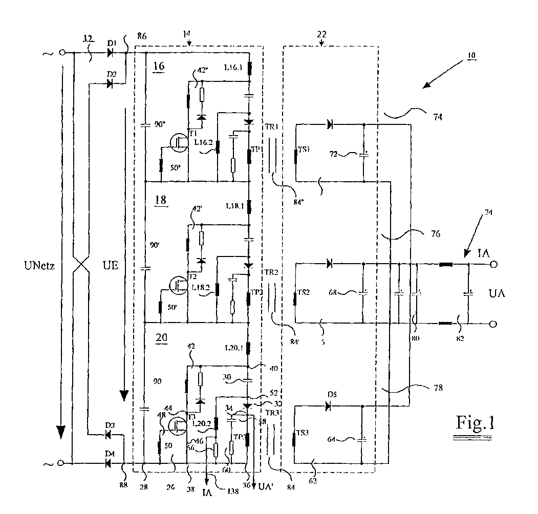
- Fig. 1 shows a current-voltage converter 10 which is connected via a diode D1 to D4 comprehensive rectifier 12 with a mains voltage U mains.
- the mains voltage U Netz in this embodiment is typically in the range from 1000 to 1500 VAC and can have a frequency of 16 2/3 Hz to 400 Hz. Input voltages in the range from 1500 VDC to 3000 VDC are also possible.
- a sinusoidally pulsating, half-wave AC input voltage U E is present at the output of the rectifier 12 and is converted into a constant output voltage U A by means of the voltage converter 10.
- the current-voltage converter 10 has a primary side 14, which has several connected in series Subsystems 16, 18, 20, each having at least one transistor circuit breaker T1, T2, T3.
- the subsystems 16, 18, 20 are in the embodiment shown here designed as SEPIC converters or regenerators, the output of each with a primary winding TP1, TP2, TP3 of an isolating transformer TR1, TR2, TR3 is.
- the isolating transformers TR1, TR2, TR3 each have secondary coils TS1, TS2, TS3 on a secondary side 22 of the voltage converter 10 to a common Load output 24 are coupled.
- the subsystem 20 comprises a SEPIC converter 26, a primary one Input 28 to which an inductor such as input choke L20.1 is connected, which via a capacitor 30 and a diode 32 with a first connection 34 of the transformer primary winding TP3 is connected. Another connection 36 is with a primary side Output 38 of the SEPIC converter 26 connected. Between the throttle on the input side L20.1 and the capacitor 30 is a connection point 40, which is connected through a ballast network 42 is connected to a first connection 44 of the transistor power switching element T3 is. Another connection 46 of the transistor circuit breaker T3 is connected to the Output 38 connected.
- a control input 48 of the transistor circuit breaker T3 is over a secondary winding of a transformer 50 is connected to the output 38.
- a junction 52 which is a second Choke L20.2 and a resistor 56 such as a shunt is connected to the output 38.
- a relief network value is as Series connection of capacitor 58 and resistor 60 arranged.
- the secondary winding TS3 of the isolating transformer TR3 is connected to a peak value rectification circuit 62 consisting of the diode D5, at the output of which a capacitor 64 is connected.
- the secondary winding TS2 is also followed by a rectification circuit 66, at the output of which a capacitor 68 is connected.
- the secondary side 22 essentially consists of three secondary systems 74, 76, 78, each consisting of the secondary transformer winding, the associated and associated rectifier and the output capacitor.
- the secondary systems 74, 76, 78 are electrically connected in parallel and form an output 80 at which the regulated output voltage U A can be tapped via a filter network 82.
- the capacitors 64, 68, 72 can also be designed as a single common capacitor with a large capacitance.
- the windings of the isolating transformers are preferably on a separate transformer core 84, 84 ', 84 ".
- the windings are preferably on a separate transformer core 84, 84 ', 84 ".
- the windings are preferably with a corresponding ratio of voltages and currents on a common core to arrange.
- the capacitors 90, 90 ', 90 " Parallel to the inputs of the respective subsystems 16, 18, 20, at the DC input, are the capacitors 90, 90 ', 90 ", at which only 1/3 of the input voltage U E drops.
- the otherwise very large storage capacitor is used withdrawn from the primary direct access to the input voltage and transformed to the low-voltage or secondary side and charged there under short-circuit current.
- a current-voltage converter 92 is shown, which via a rectifier 94 to the diode D6 - D9 is connected to the mains voltage U mains.
- the mains voltage U Netz is typically in the range from 110-234 VAC or 28-48 VAC and can have a frequency of 16 2/3 Hz - 400 Hz.
- Mains voltages in the range of 4 - 72 or 14.4 - 154 VDC are also possible.
- the current-voltage converter 92 is designed in particular for high input currents I E or output currents I A.
- the current-voltage converter 92 has a primary side 96 which has a plurality connected in parallel
- Subsystems 98, 100, 102 each have at least one transistor circuit breaker T4, T6, T7.
- the subsystems 98, 100, 102 are as shown here Embodiment designed as a SEPIC converter or regenerators, their output each with a primary winding TP4, TP5, TP6 of an isolating transformer TR4, TR5, TR6 connected is.
- the isolating transformers TR4, TR5, TR6 each have secondary coils TS4, TS5, TS6 on a secondary side 104 of the voltage-current converter 92 to one common load output 106 are coupled.
- the structure of the subsystems 98, 100, 102 essentially corresponds to the subsystems 16, 18, 20 which have been described in detail with reference to FIG. 1. Due to the primary parallel connection of the Regenaroten or SEPIC converters 98, 100, 102 with the potential separation, the current flowing through a transistor circuit breaker T4, T5, T6 is reduced to a third of the input current I E. For this reason, transistors with current resistance can be used.
- a third of the input current I E flows through each stage.
- the control transmitters 108, 110, 112 are on a common core in the parallel connection described here.
- the control transmitters 108, 110, 112 can also be designed as electronic semiconductor power drivers (not shown).
- the subsystems 98, 100, 102 have inductors L 98.1, L 100.1, L 102.1 on the input side, which are at least temporarily in parallel with the input voltage U E via the transistor circuit breakers and thus bring about a current symmetry of the overall system.
- the control of the current-voltage converter is intended to be based on the control circuit shown in FIG. 3 are explained.
- FIG. 3 shows a control loop arrangement for controlling at least one subsystem 16, 18, 20 or 98, 100, 102 of the current-voltage converter 10 or 92 according to FIG. 1 or 2.
- the control circuit 200 has a voltage comparator 202 on the input side, which has a first input 204 with a reference voltage U ARef and a second input 206 via a sampling circuit 208 such as a sample and hold circuit or continuous measurement with the output voltage U A for tapping an actual value Voltage U Alst is connected.
- the output voltage U A is measured via a measuring element (not shown) at the output 24 of the current-voltage converter or via the burden voltage U A 'at the primary transformer winding TP1-TP6 during the T OFF phase.
- An output 210 of the comparator 202 is connected to an input 212 of an amplifier 214 in order to amplify a differential voltage ⁇ U A formed from the actual voltage U Alst and the reference voltage U ARef .
- An error-amplified voltage K U x ⁇ U A is present at an output 216 of the amplifier 214 and is supplied to an input 218 of a multiplying D / A converter 220.
- Another input 222 of the D / A converter 220 is connected to an output 224 of a circuit, preferably a microcontroller 226.
- the microcontroller 226 is in turn connected via a feed line 228 to a mains line or to the mains voltage U Netz .
- the microcontroller 226 is connected via an output 230 and a trigger line 232 to an input 234 of the sampling circuit 208.
- An output 236 of the D / A converter 220, at which a target current I A target is present, is connected to an input 238 of a comparator 240.
- a further input 242 of the comparator 240 is connected via a feed line 138 to the shunt 56 in the branch of the choking coil 220.1 for tapping the output current I of a magnitude proportional A I A '.
- An output 244 of the comparator is connected to an input 246 of a current amplifier 248.
- An amplified current difference K I x ⁇ I A is present at an output 250 of the amplifier, which is fed to a control unit 252 and forms a controlled variable.
- the control unit also has an input 254 for the mains or input voltage for T ON control and an output 256 for controlling the transistor circuit breakers T1 and T6 via control transmitters 50, 50 ', 50 "and 108-112
- the T OFF time of the transistor circuit breakers T1 - T6 is regulated or controlled with the size K I x ⁇ I A. Even without a U / I controller, the T ON control and specification of the T OFF voltage as a DC variable result in a quasi-constant Output voltage with sine current consumption achieved with AC voltage supply and changing input range or output load.
- processing After recognizing and saving the time base, processing starts with a trigger zero crossing and synchronizes it with further zero crossings. Synchronization impulses, that lie between the mathematical zero crossings are due to possible Disrupted variables are hidden.
- the generated sine curve is output via the output 224 to the input 226 of the D / A converter 220.
- the sampling circuit 208 is triggered with a synchronization pulse which is present at each half-wave zero crossing.
- the error-amplified differential voltage K U x ⁇ U A is now multiplied in the D / A converter 220 by the synthetic sine curve Bmax x
- no additional correction element is required, since the measurement of the output current in the primary-side choke branch provides a variable that is independent of long-term fluctuations in the input voltage U E but follows the curve shape of the nominal frequency (PFC).
- microcontroller 226 detects that the input voltage is a Is DC voltage, a constant voltage B is output at the output 224, so that there is no PFC assessment.
- the described system of current-voltage converter 10, 92 and control circuit according to the invention 200 has four UIC voltages, particularly in the rail sector, such as Example 1000 VAC 16 2/2 Hz, 1500 VAC 50 Hz, 1500 VDC and 3000 VDC for use. Since the voltage converter or regenerator has a wide input voltage range allows the problem, whether AC input voltage or DC input voltage or which frequency the input AC voltage has, by the previously specified Features resolved. However, all four ranges as well as tolerances (+ - 30%) and long-term transients be processed in an input voltage range.
- FIG. 4 shows a current-voltage converter 400 with an independent inventive character.
- the current-voltage converter 400 has a temperature above a rectifier 404 to the mains voltage U mains primary side 402 and a secondary side 406, a plurality, that is multiple, preferably three outputs 408, 410, 412 with the output voltages U A1, U A2, U A3.
- a primary inductance such as inductor L420.1 is connected to the connection 414, which is connected via a capacitor 422 and a diode 424 to a first connection 426 of a primary-side winding TP7 of an isolating transformer TR.
- the primary-side winding TP7 is connected to the input terminal 416 of the rectifier 404 by a connection 428.
- a connection 430 which is connected to the terminal 416 via a snubber network 432 and a transistor circuit breaker T7.
- a control connection 434 of the transistor circuit breaker T7 is connected to the terminal 416 via a secondary winding 436 of a drive transformer 438.
- a connection point 440 located between the capacitor 422 and the diode 424 is likewise connected to the terminal 416 via a second inductance such as the choke coil L 420.2 and a measuring element such as shunt 444 that is connected in series with it.
- the secondary-side multiple outputs 408, 410, 412 each have a secondary winding TS7.1, TS7.2, TS7.3, which are arranged together with the primary winding TP7 on a common core 446.
- the secondary windings TS7.1, TS7.2, TS7.3 are each connected via a rectifier diode 448, 450, 452 to an output capacitor 454, 456, 458, to which the output voltage U A1 , U A2 and U A3 are applied.
- the control circuit described with reference to FIG. 3 can be used to regulate the current-voltage converter 400.
- the current-voltage converter 400 is also characterized in that feedback of control variables or monitoring functions of variables on the secondary side is not necessary. This is made possible in particular by the fact that the output voltage on the primary side can be measured at the connection 426 of the primary winding TP7 and the output current (average size) on the primary side on the measuring element 440 during the T Off time. The input voltage can be measured on the secondary side during the T On time.
Landscapes
- Engineering & Computer Science (AREA)
- Power Engineering (AREA)
- Dc-Dc Converters (AREA)
- Measuring Instrument Details And Bridges, And Automatic Balancing Devices (AREA)
- Measurement Of Current Or Voltage (AREA)
- Ignition Installations For Internal Combustion Engines (AREA)
- Details Of Television Scanning (AREA)
Abstract
Die Erfindung bezieht sich auf einen Strom-Spannungswandler (10), insbesondere für hohe
Eingangsspannungen, umfassend eine Primärseite (14), die mehrere in Reihe geschaltete
Teilsysteme (16, 18, 20) mit jeweils zumindest einem Transistor-Leistungsschalter T1, T2, T3
und jeweils einer eigenen zugeordneten Transformator-Primärwicklung TP1, TP2, TP3 aufweist,
sowie eine Sekundärseite (22), über die die Teilsysteme (16, 18, 20) an einen gemeinsamen
Lastausgang (24) angekoppelt sind. Um einen Strom-Spannungswandler mit einfachem
Aufbau und einer verbesserten Spannungssymmetrierung der Teilsysteme zur Verfügung zu
stellen, ist vorgesehen, dass die in Reihe geschalteten Teilsysteme (16, 18, 20) je einen Zweig
mit eingangsseitiger Induktivität L16.1, L18.1, L20.1 und dem zumindest einen Transistor-Leistungsschalter
T1, T2, T3 aufweisen, dass die Induktivität L16.1, L18.1, L20.1 zumindest
zeitweise über die jeweiligen Transistor-Leistungsschalter T1, T2, T3 elektrisch in Reihe an
Eingangsspannung UE liegen und eine Spannungssynunetrierung zwischen den Teilsystemen
(16, 18, 20) bewirken und dass jeweils ein Ausgang der Teilsysteme (16, 18, 20) mit jeweils
der Transformator-Primärwicklung TP1, TP2, TP3 als Trenntransformator TR1, TR2, TR3 zur
Stromspeisung verbunden ist.
Description
Die Erfindung bezieht sich einerseits auf einen Strom-Spannungswandler, insbesondere für hohe Eingangsspannungen, umfassend eine Primärseite, die mehrere in Reihe geschaltete Teilsysteme mit jeweils zumindest einem Transistor-Leistungsschalter und jeweils einer eigenen zugeordneten Transformator-Primärwicklung aufweist sowie eine Sekundärseite über die die Teilsysteme an einen gemeinsamen Lastausgang angekoppelt sind und andererseits auf einen Strom-Spannungswandler, insbesondere für hohe Eingangsströme, umfassend eine Primärseite, die mehrere parallel geschaltete Teilsysteme mit jeweils zumindest einem Transistor-Leistungsschalter und jeweils einer eigenen zugeordneten Transformator-Primärwicklung aufweist, sowie eine Sekundärseite, über die die Teilsysteme an einen gemeinsamen Lastausgang angekoppelt sind sowie auf einen zugehörigen Regelkreis, umfassend einen Spannungsregler mit Spannungsvergleicher und Spannungsverstärker sowie einen Stromregler mit Stromvergleicher und Stromverstärker sowie ein zwischen Spannungsregler und Stromregler angeordnetes Korrekturglied.The invention relates on the one hand to a current-voltage converter, in particular for high input voltages, including a primary side that has several in series Subsystems with at least one transistor circuit breaker and one each has its own assigned transformer primary winding and a secondary side which the subsystems are coupled to a common load output and on the other hand to a current-voltage converter, in particular for high input currents, comprising a Primary side, which has several subsystems connected in parallel, each with at least one Transistor circuit breakers and their own assigned transformer primary winding has, and a secondary side, via which the subsystems to a common Load output are coupled and to an associated control loop, including a Voltage regulator with voltage comparator and voltage amplifier as well as a current regulator with current comparator and current amplifier as well as between voltage regulator and current regulator arranged correction element.
Bei aus dem Stand der Technik bekannten Spannungswandlern für hohe Eingangswechselspannungen oder Gleichspannung erfolgt eine Aufschaltung eines Spitzenwertes der gleichgerichteten Spannung auf einen unmittelbar an den Ausgängen eines Gleichrichters angeordneten Kondensators mit sehr großer Kapazität. Folglich mussten sehr teure Ladeschaltungen mit Vorladung über zum Beispiel einen Widerstand und anschließende Überbrückung mit Schützkontakten realisiert werden. In voltage converters for high input AC voltages known from the prior art or DC voltage, a peak value of the rectified is applied Voltage on one located directly at the outputs of a rectifier Very large capacitance capacitor. As a result, very expensive charging circuits were required with pre-charging via, for example, a resistor and subsequent bridging with Contactor contacts can be realized.
Auch sind sogenannte "Doppelbooster"-Topologien bekannt, die einen Zwischenkreis mit einem Elektrolyt-Kodensator aufweisen, so dass dieser oder das vorgeschaltete Netz beim Aufschalten der hohen Eingangsspannung aufgrund des Durchgriffs ohne Kurzschlussstrombegrenzung belastet wird. Daher muss dieser Kondensator auf die Spitzenspannung am Eingang ausgelegt sein, die höher als die geregelte Ausgangsspannung des Boosters ist.So-called "double booster" topologies are also known which have an intermediate circuit have an electrolyte code, so that this or the upstream network Applying the high input voltage due to the penetration without short-circuit current limitation is charged. Therefore, this capacitor must be at the peak voltage at the input be designed, which is higher than the regulated output voltage of the booster.
Auch treten bei der Beherrschung hoher Eingangsspannungen und Ströme bezüglich der verwendeten Bauelemente Probleme auf. So müssen die verwendeten Halbleiter wie Transistoren und Dioden an die maximale Eingangsspannung oder Strom angepasst werden und die verwendeten Transformatoren müssen sowohl leistungs- als auch spannungsmäßig an die zu verarbeitende Eingangsspannung angepasst werden, wobei nicht vertretbare Windungs- und Wicklungsspannungen auftreten.Also, when mastering high input voltages and currents, the used components problems. So the semiconductors used must be like transistors and diodes can be adapted to the maximum input voltage or current and the The transformers used must match both the power and voltage Processing input voltage are adjusted, whereby unacceptable winding and Winding voltages occur.
Bei bekannten Wandlern, die Leistungstransistoren als Schaltelemente benutzen, ist die zulässige Eingangsspannung durch die Spannungsbelastbarkeit des verwendeten Leistungstransistortyps begrenzt. Bei einer Reihen- /Parallelschaltung mehrerer, synchron getakteter Transistoren stellt sich das Problem der Spannungs- /Stromsymmetrierung, wozu zum Beispiel die Anbringung verlustbehafteter RCD-Leitungszweige parallel zur Transistorschalt- strecke bekannt ist.In known converters that use power transistors as switching elements, the permissible input voltage due to the voltage carrying capacity of the power transistor type used limited. With a series / parallel connection of several, synchronously clocked Transistors face the problem of voltage / current balancing, for example the installation of lossy RCD line branches parallel to the transistor switching path is known.
In der DE 44 14 677 A1 wird ein primärgetakteter Spannungswandler vorgeschlagen, dessen Primärseite aus mehreren, seriell aneinandergeschalteten Teilsystemen aufgebaut ist, die jeweils eine Transistor-Leistungsschalteranordnung beinhalten, denen jeweils eine eigene Transformator-Primärwicklung zugeordnet ist, welche über die Sekundärseite des Wandlers an einen gemeinsamen Lastausgang angekoppelt sind. Die Kopplung bewirkt über die Transformator-Wicklungsspannung eine automatische, dynamische und quasi verlustfreie Spannungssymmetrierung zwischen den Teilsystemen im Lastbetrieb.DE 44 14 677 A1 proposes a primary clocked voltage converter, the The primary side is made up of several subsystems connected in series, which each contain a transistor circuit breaker arrangement, each of which has its own Transformer primary winding is assigned, which is on the secondary side of the converter are coupled to a common load output. The coupling causes the Transformer winding voltage an automatic, dynamic and quasi lossless Voltage symmetry between the subsystems in load operation.
Bei dieser Ausführungsform sind die Transformatorwicklungen sekundärseitig "hart"-parallel geschaltet. Dadurch ergibt sich der Nachteil, dass Unsymmetrien zu nicht strombegrenzten dynamischen Ausgleichströmen führen, die aber erst die Symmetrierung bewirken. In this embodiment, the transformer windings are "hard" parallel on the secondary side switched. This has the disadvantage that asymmetries with non-current-limited ones lead dynamic balancing currents, but which only bring about the symmetrization.
Auch ist diese Schaltungsanordnung mit dem Nachteil behaftet, dass bei Wandlern mit Wechselspannungseingang eine Aufschaltung des Spitzwertes der gleichgerichteten Spannung auf einen direkt am Ausgang eines Gleichrichters angeordneten Kondensator mit sehr großer Kapazität erfolgt und alle diese Durchflusswandlertopologien keine der Eingangsspannungs-Kurvenform angepasste Stromaufnahme (Power Factor Correction PFC) zulassen.This circuit arrangement also has the disadvantage that with converters AC voltage input a connection of the peak value of the rectified voltage to a very large capacitor directly at the output of a rectifier Capacitance occurs and all of these forward converter topologies have none of the input voltage waveform Allow adjusted current consumption (Power Factor Correction PFC).
Der vorliegenden Erfindung liegt daher das Problem zu Grunde, einen Wandler für hohe Eingangsspannungen oder -Ströme zur Verfügung zu stellen, der einen einfachen Aufbau aufweist und dessen Spannungs- oder Stromsymmetrierung verbessert wird.The present invention is therefore based on the problem of a converter for high To provide input voltages or currents of simple construction has and the voltage or current symmetry is improved.
Das Problem wird bei einem Wandler, insbesondere für hohe Eingangsspannungen, erfindungsgemäß dadurch gelöst, dass die in Reihe geschalteten Teilsysteme je einen Zweig mit eingangsseitiger Induktivität und dem zumindest einen Transistor-Leistungsschalter aufweisen, wobei die Induktivitäten zumindest zeitweise über die jeweiligen Transistor-Leistungsschalter elektrisch in Reihe an Eingangsspannung liegen und eine Spannungssymmetrierung zwischen den Teilsystemen bewirken und wobei jeweils ein Ausgang der Teilsysteme mit jeweils der Transformator-Primärwicklung als Trenntransformator zur Stromspeisung verbunden ist.The problem is solved according to the invention in the case of a converter, in particular for high input voltages solved in that the subsystems connected in series each have a branch have inductance on the input side and the at least one transistor power switch, the inductances at least temporarily via the respective transistor power switches electrically in series at the input voltage and a voltage symmetry between cause the subsystems and where an output of the subsystems with each Transformer primary winding is connected as an isolating transformer for power supply.
Das Problem wird bei einem Wandler, insbesondere für hohe Eingangsströme, erfindungsgemäß dadurch gelöst, dass die parallel geschalteten Teilsysteme je einen Zweig mit einer eingangsseitigen Induktivität und dem zumindest einen Transistor-Leistungsschalter aufweisen, der zumindest zeitweise über die jeweiligen Transistor-Leistungsschalter elektrisch parallel an Eingangsspannung UE liegt und eine Stromsymmetrierung zwischen den Teilsystemen bewirkt und dass jeweils ein Ausgang der Teilsysteme mit jeweils der Transformator-Primärwicklung als Trenntransformator zur Stromspeisung verbunden ist.In a converter, in particular for high input currents, the problem is solved according to the invention in that the subsystems connected in parallel each have a branch with an inductor on the input side and the at least one transistor circuit breaker, which at least at times at times electrically parallel to the input voltage via the respective transistor circuit breaker U E lies and causes a current symmetry between the subsystems and that in each case one output of the subsystems is connected to each of the transformer primary winding as an isolating transformer for power supply.
Diese Topologie bewirkt eine - im Gegensatz zu den bekannten Systemen - Stromspeisung in den Transformator. Das heisst, dass jede Primärwicklung seinen Strom im Durchflusskonzept überträgt und somit auf die sekundäre Bürde einprägt.In contrast to the known systems, this topology causes a power supply in the transformer. This means that each primary winding has its current in the flow concept transfers and thus impresses on the secondary burden.
Durch zeitsynchrones Ansteuern aller in den Teilsystemen angeordneten Transistor-Leistungsschalter arbeitet jedes Teilsystem mit einer Teilspannung bzw. einem Teilstrom, die bzw. der sich aus der Eingangsspannung UE bzw. Eingangsstrom IE dividiert durch die Anzahl N der in Reihe oder parallel geschalteten Teilsysteme ergibt. Insofern können sowohl für die Auslegung der Transistoren-Leistungsschalter als auch für die Auslegung der Induktivitäten wie Drosselspulen und Trenn-Transformatoren handelsübliche Bauelemente verwendet werden, die nicht Hochspannungsanforderungen genügen müssen. Die Kosten reduzieren sich dadurch erheblich. Wesentlicher Unterschied zu dem Schaltungsaufbau gemäß Stand der Technik ist, dass die Strom-/Spannungssymmetrierung über die eingangsseitige bzw. primärseitige Induktivität bzw. Drosselspule des jeweiligen Teilsystems stattfindet. Unter der Voraussetzung, dass sämtliche zeitweilig in Reihe oder parallel liegenden Drosselspulen die gleiche Induktivität aufweisen und ein synchrones Ansteuem gewährleistet ist, fällt an jeder für eine bestimmte Zeit vom Strom durchflossenen Drosselspule einerseits bei Reihenschaltung ein gleicher Spannungsabfall ab, so dass auch die über den Schaltelementen anliegende Spannung einem N-ten Teil der Eingangsspannung UE entspricht und andererseits fällt bei Parallelschaltung ein gleicher Stromanteil ab, so dass auch die durch die Schaltelemente fließenden Ströme einen N-ten Teil des Eingangsstromes entsprechen.By synchronously triggering all transistor circuit breakers arranged in the subsystems, each subsystem works with a subvoltage or a subcurrent which results from the input voltage U E or input current I E divided by the number N of subsystems connected in series or in parallel . In this respect, commercially available components that do not have to meet high-voltage requirements can be used both for the design of the transistor circuit breakers and for the design of the inductances such as inductors and isolating transformers. This significantly reduces costs. The essential difference from the circuit structure according to the prior art is that the current / voltage symmetry takes place via the input-side or primary-side inductor or choke coil of the respective subsystem. Provided that all inductors that are temporarily in series or in parallel have the same inductance and that synchronous control is ensured, the same voltage drop will drop at each inductor through which the current flows for a certain time when connected in series, so that the voltage across the switching elements also applied voltage corresponds to an Nth part of the input voltage U E and, on the other hand, an equal current component drops when connected in parallel, so that the currents flowing through the switching elements also correspond to an Nth part of the input current.
Bei einer besonders bevorzugten Ausführungsform ist vorgesehen, dass die Teilsysteme als SEPIC-Wandler oder Regenerator ausgebildet sind, wobei zumindest ein Wandler, vorzugsweise der mit Bezugspotential (Masse) verbundene Wandler, mit nur einem Regelkreis verbunden ist, dessen Ausgangssignal mit einer allen Transistor-Leistungsschaltern zugeordneten Ansteuerschaltung verbunden ist.In a particularly preferred embodiment it is provided that the subsystems as SEPIC converter or regenerator are formed, at least one converter, preferably the converter connected to reference potential (ground), connected to only one control loop is, the output signal associated with all transistor circuit breakers Control circuit is connected.
Bei einer weiteren besonderen Ausführungsform ist vorgesehen, dass der Regelkreis einen mit
der Netzspannung verbundenen Schaltkreis zur Erfassung der Netzspannung und/oder der
Netzfrequenz aufweist und entsprechende Signale an den Regelkreis weitergibt, so dass der
Spannungswandler in Abhängigkeit von der Eingangsspannung entweder als DC-Wandler
oder auch als AC-Wandler mit PFC-Bewertung arbeitet. Durch den Einsatz einer mit der
Netzleitung verbundenen Erkennungsschaltung wird ein großer Einsatzbereich des Spannungswandlers
ermöglicht. Dadurch kann das Spannungswandlersystem speziell im Bahnbereich
an zumindest vier UIC-Spannungen (1000 VAC 16 2/3 Hz; 1500 VAC 50 Hz; 1500
VDC; 3000 VDC) betrieben werden.In a further particular embodiment, it is provided that the control loop has a
the mains voltage connected circuit for detecting the mains voltage and / or
Mains frequency and corresponding signals to the control loop, so that the
Voltage converter depending on the input voltage either as a DC converter
or also works as an AC converter with PFC evaluation. By using one with the
Detection circuit connected to the power line becomes a large area of application for the voltage converter
enables. This enables the voltage converter system to be used especially in the railway sector
at at least four UIC voltages (1000
Das neuartige Spannungswandlersystem ist daher in der Lage, sich an verschiedene Eingangsspannungen und/oder Frequenzen mit der Stromaufnahme anzupassen. Auch wird ermöglicht, dass Regelparameter auf die jeweilige Nennspannung voreingestellt werden können.The new voltage converter system is therefore able to adapt to different input voltages and / or adapt frequencies with the current consumption. It also enables that control parameters can be preset to the respective nominal voltage.
Zur PFC-Bewertung ist vorgesehen, dass zumindest einer weiteren, mit der eingangsseitigen Drosselspule magnetisch gekoppelten Drosselspule ein Messelement wie Shunt zugeordnet ist, an dem eine dem Ausgangsstrom IA proportionale Größe IA', vorzugsweise DC-Größe,-abgreifbar ist. Auch hier ergibt sich wiederum der Vorteil, dass eine PFC-Regelung bei beliebiger Eingangswechselspannung möglich ist. Das Messelement ist vorzugsweise in dem mit Bezugspotential verbundenen Teilsystem angeordnet. Die Größe IA' kann auch einen AC-Anteil aufweisen, der proportional zum Eingangsstrom IE ist, d. h. einer Sinushalbwellenfunktion erfolgt.For PFC evaluation, it is provided that at least one further choke coil magnetically coupled to the input-side choke coil is assigned a measuring element such as a shunt, on which a variable I A ', preferably a DC variable, proportional to the output current I A can be tapped. Here again there is the advantage that PFC control is possible with any input AC voltage. The measuring element is preferably arranged in the subsystem connected to the reference potential. The variable I A 'can also have an AC component which is proportional to the input current I E , that is to say a sine half-wave function.
Ein weiterer Vorteil des Einsatzes von SEPIC-Wandlern in dem hier vorgestellten Spannungswandlersystem ist darin begründet, dass der ansonsten übliche primäre Speicherkondensator am Ausgang des Gleichrichters oder im Zwischenkreis auf die Niedervoltseite bzw. Sekundärseite transformiert und dort kurzschlussstromgeregelt aufgeladen wird. Dadurch wird der ansonsten vorhandene Speicherkondensator dem primären direkten Zugriff der Eingangsspannung entzogen. Aus diesem Grunde kann auf Elektrolyte am Eingang verzichtet werden (Hochvoltkreis) und die Elektrolyte werden in den Sekundärkreis (Niedervoltkreis) transformiert. Im Sekundärkreis können preiswerte Elektrolytkondensatoren eingesetzt werden.Another advantage of using SEPIC converters in the voltage converter system presented here is due to the fact that the otherwise usual primary storage capacitor at the output of the rectifier or in the intermediate circuit on the low voltage side or Secondary side is transformed and there is charged short-circuit current controlled. This will the otherwise existing storage capacitor provides primary direct access to the input voltage withdrawn. For this reason, there is no need for electrolytes at the entrance (High-voltage circuit) and the electrolytes are transformed into the secondary circuit (low-voltage circuit). Inexpensive electrolytic capacitors can be used in the secondary circuit.
Durch die eingangsseitige Reihen- oder Parallelschaltung der die Trenntransformatoren ansteuernden Wandler können die Wandler selbst auf 1/N-fache Gesamtleistung ausgelegt sein, wobei N der Anzahl der in Reihe oder parallel geschalteten Teilsysteme entspricht.By connecting the isolating transformers in series or parallel on the input side Converters, the converters themselves can be designed for 1 / N times the total power, where N corresponds to the number of subsystems connected in series or in parallel.
Auch die Windungsspannung bzw. der Wicklungsstrom der einzelnen Strom-Trenntransformatoren kann entsprechend geringer ausgelegt werden. Also the winding voltage or the winding current of the individual current isolating transformers can be designed accordingly lower.
Bei einer bevorzugten Ausführungsform ist vorgesehen, dass die Ausgangsspannung des Strom-Spannungswandler-Systems auf verschiedene Ausgangsspannungen einstellbar ist. Dies wird insbesondere aufgrund der Ansteuerung der in den Teilsystemen angeordneten Transistor-Leistungsschalter bewirkt. Auch besteht die Möglichkeit einer Primärwicklung auf einem Kern mehrere Sekundärwicklungen unterschiedlicher Windungszahlen zuzuordnen.In a preferred embodiment it is provided that the output voltage of the Current-voltage converter system is adjustable to different output voltages. This is particularly due to the control of the transistor circuit breakers arranged in the subsystems causes. There is also the possibility of a primary winding on one Core to assign several secondary windings of different number of turns.
Es ist vorgesehen, dass die in den Teilsystemen enthaltenen Transistor-Leistungsschalter über auf einen gemeinsamen Kern angeordnete Übertrager ansteuerbar sind, wodurch ein zeitsynchrones Ansteuern der in Reihe oder parallel geschalteten Transistor-Leistungsschalter sichergestellt ist. Des Weiteren ist vorgesehen, dass die Primär-Wicklung des Trenntransformators über eine Diode an einen jeweiligen Ausgang der SEPIC-Wandler angekoppelt ist. Dadurch wird sichergestellt, dass Rückströme des Trenntransformators keine negativen Auswirkungen auf den SEPIC-Wandler haben und der Strom-Trenntransformator freier entmagnetisieren kann.It is envisaged that the transistor circuit breakers contained in the subsystems via arranged on a common core can be controlled, making a time-synchronous Control of the transistor circuit breakers connected in series or in parallel is ensured. It is also provided that the primary winding of the isolating transformer the SEPIC converter is coupled via a diode to a respective output. This ensures that reverse currents from the isolating transformer are not negative Affect the SEPIC converter and the current isolating transformer freer can demagnetize.
Des Weiteren ist vorgesehen, dass die Primärwicklungen auf einen gemeinsamen Kern gewickelt werden und auf eine Sekundärwicklung arbeiten.Furthermore, it is provided that the primary windings on a common core be wound and work on a secondary winding.
Erfindungsgemäß wird weiterhin ein Regelkreis für einen Strom-Spannungswandler vorgeschlagen, umfassend einen Spannungsregler mit Spannungsvergleicher und Spannungsverstärker sowie einen Stromregler mit Stromvergleicher und Stromverstärker sowie ein zwischen Spannungsregler und Stromregler angeordnetes Korrekturglied.According to the invention, a control loop for a current-voltage converter is also proposed, comprising a voltage regulator with voltage comparator and voltage amplifier as well as a current regulator with current comparator and current amplifier as well as a between Voltage regulator and current regulator arranged correction element.
Der Regelkreis weist einen Schaltkreis zur Erfassung der Netzspannung und/oder Netzfrequenz auf, wobei der Schaltkreis mit einer Abtastschaltung verbunden ist, die mit einem Eingang an Ausgangsspannung liegt und mit einem Ausgang mit dem ersten Eingang eines Spannungsvergleichers verbunden ist und wobei der Spannungsregler ausgangsseitig mit einem vorzugsweise multiplizierendem D/A-Wandler verbunden ist, der seinerseits mit einem zweiten Eingang mit einem Ausgang des Schaltkreises verbunden ist und ausgangsseitig mit einem Eingang des Stromvergleichers des Stromreglers verbunden ist. The control circuit has a circuit for detecting the line voltage and / or line frequency on, the circuit being connected to a sampling circuit connected to a Input is at output voltage and with an output with the first input one Voltage comparator is connected and the voltage regulator on the output side a preferably multiplying D / A converter, which in turn is connected to a second input is connected to an output of the circuit and on the output side is connected to an input of the current comparator of the current regulator.
Durch die Erkennung von Netzspannung und Netzfrequenz kann der Regelkreis auf verschiedene Eingangsspannungen und/oder -frequenzen eingestellt werden. Die entsprechenden Regelparameter werden durch den Schaltkreis zur Verfügung gestellt. Eine PFC-Bewertung kann somit bei beliebiger Eingangswechselspannung (Amplitude, Bereich und Frequenz) durchgeführt werden. Alternativ kann auch die gleichgerichtete Eingangsspannung (nach dem Gleichrichter) abgetastet bzw. erfasst werden.The control loop can be set to different values by detecting the line voltage and line frequency Input voltages and / or frequencies can be set. The corresponding Control parameters are provided by the circuit. A PFC assessment can therefore with any input AC voltage (amplitude, range and frequency) be performed. Alternatively, the rectified input voltage (after the Rectifier) can be sampled or recorded.
Um eine genaue Ermittlung der Netzspannung und der Netzfrequenz zu gewährleisten - die Netzspannung kann auch eine DC-Spannung sein - ist der Schaltkreis als integrierte Schaltung, vorzugsweise als Mikrocomputer bzw. Mikrocontroler ausgebildet. In Abhängigkeit der ermittelten Netzparameter wird eine synthetische Funktion mit konstanter Amplitude B (bei DC-Eingang) oder eine pulsierende Sinusfunktion B max | sin (ω t)| (bei AC-Eingang) in Phase und synchron mit dem Netzeingang zur Verfügung gestellt, der die tatsächliche synchronisierte Netzfrequenz repräsentiert. Die an dem Ausgang des Spannungsverstärkers anliegende fehlerverstärkte Spannungsdifferenz ku x ΔUA kann sodann mit der am Ausgang des Mikrocontrolers zur Verfügung gestellten digitalen Sinusfunktion multipliziert werden. Dazu ist dem Spannungsverstärker der D/A-Wandler nachgeschaltet, dem der digitale Sinus des Schaltkreises zugeführt wird. Am Ausgang des D/A-Wandlers ist eine sinusmodulierte fehlerverstärkte Spannung abgreifbar, die als Sollwert für den nachgeschalteten Strom-Regelkreis zur Verfügung steht.In order to ensure a precise determination of the mains voltage and the mains frequency - the mains voltage can also be a DC voltage - the circuit is designed as an integrated circuit, preferably as a microcomputer or microcontroller. Depending on the determined network parameters, a synthetic function with constant amplitude B (with DC input) or a pulsating sine function B max | sin (ω t) | (with AC input) in phase and in sync with the mains input, which represents the actual synchronized mains frequency. The error-amplified voltage difference k u x ΔU A present at the output of the voltage amplifier can then be multiplied by the digital sine function provided at the output of the microcontroller. To this end, the voltage amplifier is followed by the D / A converter, to which the digital sine of the circuit is fed. A sine-modulated error-amplified voltage can be tapped at the output of the D / A converter and is available as a setpoint for the downstream current control circuit.
Vorteil der neuartigen Regelkreisanordnung ist, dass eine Korrektur aufgrund von Eingangsspannungsänderungen nicht notwendig ist. Insbesondere benötigt das Korrekturglied keine Korrektur als Funktion der Eingangsspannung UE Auch der dem Regelkreis zugeführte Ist-Strom IAlst ist unabhängig von Schwankungen der Eingangsspannung UE.The advantage of the new control loop arrangement is that a correction due to input voltage changes is not necessary. In particular, the correction element does not require a correction as a function of the input voltage U E. The actual current I Alst supplied to the control loop is also independent of fluctuations in the input voltage U E.
Es ist vorgesehen, dass in dem Schaltkreis vorprogrammierte Sinusfunktionen abgelegt sind, wobei die digitalen Werte in dem den Spannungsverstärker nachgeschalteten D/A-Wandler multipliziert und verrechnet werden.It is provided that preprogrammed sine functions are stored in the circuit, the digital values in the D / A converter connected downstream of the voltage amplifier be multiplied and offset.
Auch ist vorgesehen, dass der in dem Schaltkreis erzeugte synthetische Sinus als Referenz für eine kontinuierliche Unter- bzw. Überspannungserkennung herangezogen wird.It is also provided that the synthetic sine generated in the circuit serves as a reference for continuous undervoltage or overvoltage detection is used.
Des Weiteren weist der Regelkreis eine in dem Schaltkreis integrierte Komparatorschaltung auf, mit der der am Ausgang des Schaltkreises anliegende synthetische Sinus zum Netz synchronisiert wird.Furthermore, the control circuit has a comparator circuit integrated in the circuit with which the synthetic sine present at the output of the circuit synchronizes with the network becomes.
Weist die Netzspannung keine Nulldurchgänge auf, d. h. es handelt sich um eine Eingangsgleichspannung, so gibt der Schaltkreis einen konstanten Wert B aus, so dass der Regelkreis als DC-Regelkreis arbeitet und eine PFC-Bewertung in diesem Fall nicht stattfindet.If the mains voltage has no zero crossings, i. H. it is an input DC voltage, so the circuit outputs a constant value B, so the control loop works as a DC control loop and a PFC evaluation does not take place in this case.
Durch die obigen Maßnahmen kann der Einsatzbereich des Spannungswandlersystems
erheblich erweitert werden, so dass speziell im Bahnbereich zumindest vier UIC-Spannungen
(1000 VAC 16 2/3 Hz, 1500 VAC 50 Hz, 1500 VDC, 3000 VDC) oder 48/60/110/220V DC
und 110/234 VAC 60/50 Hz Netze als Einspannungsbereichswandler beherrschbar sind. Da
der Wandler bzw. Regenerator sehr weite Eingangsspannungsbereiche zulässt, wird die
Problematik, ob DC-Eingangsspannung oder AC-Eingangsspannung mit verschiedener
Frequenz durch vorgenannten Lösungsweg gelöst, so dass alle vier Spannungsbereiche plus
Toleranzen (+/- 30 %) und Langzeittransienten in einem Eingangsspannungsbereich abgearbeitet
werden können. Auch DC-Eingangsspannungen mit besonders hohem Wechselspannungsanteil
vorzugsweise ohne Spitzenströme sind beherrschbar. Auch besteht die
Möglichkeit, dass einige Regelparameter auf die Nennspannung voreinstellbar sind (Ton-Zeit).The application of the voltage converter system can be done by the above measures
considerably expanded, so that at least four UIC voltages, especially in the railway sector
(1000
Verfahrensmäßg zeichnet sich die Erfindung dadurch aus, dass die primären Teilsysteme im nichtstromlückenden Betrieb betrieben werden und erstmalig eine Kaskadierung solcher Teilsysteme erfolgt. Bei den Teilsystemen handelt es sich nämlich um "drosselbewertete" Topologien, die zum Eingang hin nicht stromlückend sind. Auch wird erfindungsgemäß die PFC-Bewertung der kaskadierten Teilsysteme einstufig an nur einem Teilsystem durchgeführt, wodurch jedoch das Gesamtsystem PFC-bewertet wird.In procedural terms, the invention is characterized in that the primary subsystems in non-current-gap operation and for the first time cascading such Subsystems done. The subsystems are namely "throttle-rated" Topologies that do not have current gaps towards the entrance. According to the invention, too PFC evaluation of the cascaded subsystems carried out in one stage on only one subsystem, whereby, however, the overall system is PFC-rated.
Verfahrensmäßig ist eine Rückführung von Regelgrößen oder Überwachungsfunktionen mit aufwendigen potentialtrennenden Maßnahmen nicht erforderlich. Dies wird dadurch erreicht, dass der Ausgangsstrom als Average-Größe auf der Primärseite messbar ist. Auch kann die Ausgangsspannung primärseitig während der TOff -Zeit an der primärseitigen Transformatorwicklung gemessen werden. Vorteilhaft kann die Eingangsspannung UE während der TOn-Zeit sekundärsseitig an einer sekundären Wicklung gemessen werden.In terms of procedure, feedback of control variables or monitoring functions with complex potential-isolating measures is not necessary. This is achieved in that the output current can be measured as an average variable on the primary side. The output voltage on the primary side can also be measured on the primary-side transformer winding during the T Off time. The input voltage U E can advantageously be measured on the secondary side on a secondary winding during the T On time.
Eine Korrektur des Regelkreises über die Eingangsspannung UE, wie sie bei den Regelkreisen gemäß dem Stand der Technik bekannt ist, kann bei dem erfindungsgemäßen Regelkreis entfallen, da die Netzspannung/Eingangsspannung durch den Schaltkreis vorgegeben wird und die dem Ausgangsstrom proportionale Größe von Schwankungen der Eingangsspannung unabhängig ist.A correction of the control loop via the input voltage U E , as is known in the control loops according to the prior art, can be omitted in the control loop according to the invention, since the mains voltage / input voltage is predetermined by the circuit and the magnitude of fluctuations in the input voltage proportional to the output current is independent.
Des Weiteren wird ein Strom-Spannungswandler gemäß Anspruch 25 mit eigenständigem Erfindungscharakter vorgestellt, der primärseitig im wesentlichen den Aufbau eines Teilsystems der bereits beschriebenen kaskadierten Strom-Spannungswandler aufweist, jedoch ausgangsseitig multiple Ausgänge aufweist mit separaten Sekundärwicklungen, die über einen gemeinsamen Kern von der Primärwicklung bestromt werden. Aufgrund der Stromspeisung des Trenntransformators bestimmen sich die Ausgangsspannungen der multiplen Ausgänge allein aus dem Wicklungsverhältnis der Windungszahlen von Primär- zu Sekundärwicklung. Die einzelnen Ströme teilen sich entsprechend dem Innenwiderstand der Last auf die einzelnen Ausgänge auf. Daher sind die Ausgangsspannungen auch bei sich ändernden Lastströmen konstant.Furthermore, a current-voltage converter according to claim 25 with independent Invention character presented, the primary side essentially the structure of a subsystem the cascaded current-voltage converter already described, however has multiple outputs on the output side with separate secondary windings connected via a common core are energized by the primary winding. Because of the power supply The isolating transformer determines the output voltages of the multiple outputs solely from the winding ratio of the number of turns from primary to secondary winding. The individual currents are divided among the individual according to the internal resistance of the load Outputs on. Therefore, the output voltages are also with changing load currents constant.
Auch hierbei wir der Strom-Spannungswandler im nicht stromlückenden Betrieb betrieben. Die Ausgangsgrößen sind wiederum primärseitig meßbar und dem zuvor beschriebenen Regelkreis zuzuführen.Here, too, the current-voltage converter is operated in non-current-gap operation. The output variables are in turn measurable on the primary side and the one described above Control loop.
Alternativ kann eine Zusatzwicklung oder eine Sekundärwicklung und/oder die Primärwicklung selbst als Messwicklung ausgebildet sein, um Signale für den Regelkreis zur Verfügung zu stellen.Alternatively, an additional winding or a secondary winding and / or the primary winding itself be designed as a measuring winding to provide signals for the control loop to deliver.
Weitere Einzelheiten, Vorteile und Merkmale der Erfindung ergeben sich nicht nur aus den Ansprüchen, den diesen zu entnehmenden Merkmalen - für sich und/oder in Kombination -, sondern auch aus der nachfolgenden Beschreibung von den Figuren zu entnehmenden bevorzugten Ausführungsbeispielen.Further details, advantages and features of the invention result not only from the Claims, the features to be extracted from these - individually and / or in combination -, but also preferred from the following description of the figures Embodiments.
Es zeigen:
- Fig. 1
- einen kaskadierten Strom-Spannungswandler mit drei primärseitig in Reihe geschalteten Teilsystemen, wobei die Teilsysteme als SEPIC-Wandler ausgebildet sind,
- Fig. 2
- einen Strom-Spannungswandler mit drei primärseitig parallel geschalteten Teilsystemen,
- Fig. 3
- eine Regelkreisanordnung für zumindest ein Teilsystem des Spannungswandlersystems gemäß Fig. 1 oder Fig. 2 und
- Fig. 4
- einen Strom-Spannungswandler mit sekundärseitig multiplen Ausgängen.
- Fig. 1
- a cascaded current-voltage converter with three subsystems connected in series on the primary side, the subsystems being designed as SEPIC converters,
- Fig. 2
- a current-voltage converter with three subsystems connected in parallel on the primary side,
- Fig. 3
- a control loop arrangement for at least one subsystem of the voltage converter system according to FIG. 1 or FIG. 2 and
- Fig. 4
- a current-voltage converter with multiple outputs on the secondary side.
Fig. 1 zeigt einen Strom-Spannungswandler 10, der über einen Dioden D1 bis D4 umfassenden
Gleichrichter 12 mit einer Netzspannung UNetz verbunden ist. Die Netzspannung UNetz liegt
bei dieser Ausführungsform typisch im Bereich von 1000 bis 1500 VAC und kann eine Frequenz
von 16 2/3 Hz bis 400 Hz aufweisen. Auch sind Eingangsspannungen im Bereich von
1500 VDC bis 3000 VDC möglich. Am Ausgang des Gleichrichters 12 liegt in dem hier
dargestellten Ausführungsbeispiel eine sinusförmig pulsierende, halbwellenförmige Eingangswechselspannung
UE an, die mittels des Spannungswandlers 10 in eine konstante Ausgangsspannung
UA umgewandelt wird.Fig. 1 shows a current-
Der Strom-Spannungswandler 10 weist eine Primärseite 14 auf, die mehrere in Reihe geschaltete
Teilsysteme 16, 18, 20 aufweist, die jeweils zumindest einen Transistor-Leistungsschalter
T1, T2, T3 aufweisen. Die Teilsysteme 16, 18, 20 sind in dem hier dargestellten Ausführungsbeispiel
als SEPIC-Wandler bzw. Regeneratoren ausgebildet, deren Ausgang jeweils mit
einer Primärwicklung TP1, TP2, TP3 eines Trenntransformators TR1, TR2, TR3 verbunden
ist. Die Trenntransformatoren TR1, TR2, TR3 weisen jeweils Sekundärspulen TS1, TS2, TS3
auf, die über eine Sekundärseite 22 des Spannungswandlers 10 an einen gemeinsamen
Lastausgang 24 angekoppelt sind.The current-
Im Folgenden wird beispielhaft der Aufbau eines SEPIC-Wandlers anhand des Teilsystems
20 beschrieben. Das Teilsystem 20 umfasst einen SEPIC-Wandler 26, einen primärseitigen
Eingang 28 an dem eine Induktivität wie Eingangsdrossel L20.1 angeschlossen ist, die über
einen Kondensator 30 und eine Diode 32 mit einem ersten Anschluss 34 der Transformator-primärwicklung
TP3 verbunden ist. Ein weiterer Anschluss 36 ist mit einem primärseitigen
Ausgang 38 des SEPIC-Wandlers 26 verbunden. Zwischen der eingangsseitigen Drossel
L20.1 und dem Kondensator 30 liegt eine Verbindungsstelle 40, die über ein Vorschaltnetzwerk
42 mit einem ersten Anschluss 44 des Transistor-Leistungsschaltelementes T3 verbunden
ist. Ein weiterer Anschluss 46 des Transistor-Leistungsschalters T3 ist mit dem
Ausgang 38 verbunden. Ein Steuereingang 48 des Transistor-Leistungsschalters T3 ist über
eine Sekundärwicklung eines Übertragers 50 mit dem Ausgang 38 verbunden. Zwischen dem
Kondensator 30 und der Diode 32 liegt eine Verbindungsstelle 52, die über eine zweite
Drossel L20.2 und einen Widerstand 56 wie Shunt mit dem Ausgang 38 verbunden ist.
Parallel zu der primärseitigen Transformatorwicklung TP3 ist ein Entlastungsnetzwert als
Reihenschaltung aus Kondensator 58 und Widerstand 60 angeordnet.The following is an example of the structure of a SEPIC converter based on the subsystem
20 described. The subsystem 20 comprises a
Sekundärseitig ist die Sekundärwicklung TS3 des Trenntransformators TR3 mit einer Spitzenwert-Gleichrichtschaltung
62 bestehend aus der Diode D5 verbunden, an dessen Ausgang ein
Kondensator 64 liegt. Der Sekundärwicklung TS2 ist ebenfalls eine Gleichrichtschaltung 66
nachgeschaltet, an deren Ausgang ein Kondensator 68 liegt. Gleiches gilt für die Sekundärwicklung
TS1, der eine Gleichrichtschaltung 70 nachgeschaltet ist, an dessen Ausgang ein
Kondensator 72 liegt. Die Sekundärseite 22 besteht im wesentlichen aus drei Sekundärsystemen
74, 76, 78, bestehend aus jeweils der sekundären Transformatorwicklung, dem zugehörigen
und zugeordneten Gleichrichter und dem Ausgangskondensator. Die Sekundärsysteme
74, 76, 78 sind elektrisch parallel geschaltet und bilden einen Ausgang 80, an dem über
ein Filternetzwerk 82 die geregelte Ausgangsspannung UA abgreifbar ist. Die Kondensatoren
64, 68,72 können auch als einzelner gemeinsamer Kondensator mit großer Kapazität ausgelegt
werden. On the secondary side, the secondary winding TS3 of the isolating transformer TR3 is connected to a peak value rectification circuit 62 consisting of the diode D5, at the output of which a
Vorzugsweise sind die Wicklungen der Trenntransformatoren auf einen separaten Transformatorkern
84, 84', 84" angeordnet. Altemativ besteht jedoch die Möglichkeit, die Wicklungen
bei entsprechendem Verhältnis der Spannungen und Ströme auf einem gemeinsamen Kern
anzuordnen.The windings of the isolating transformers are preferably on a
Durch die primärseitige Reihenschaltung der Regeneratoren bzw. SEPIC-Wandler mit
Potentialtrennung reduziert sich die an einem Transistor-Leistungsschalter T1, T2, T3 abfallende
Spannung auf ein Drittel der Eingangsspannung UE. Aus diesem Grund können
Transistoren mit handelsüblicher Spannungsfestigkeit eingesetzt werden. Durch zeitsynchrones
Ansteuern der primärseitigen Teilsysteme 16, 18, 20 über die Übertrager 50, 50', 50" liegt
jede Stufe an einem Drittel der Eingangsspannung UE. Um ein zeitsynchrones Ansteuem zu
erreichen, sind Ansteuer-Wicklungen der Übertrager 50, 50', 50" der auf einem gemeinsamen
magnetischen Kern angeordnet. Alternativ besteht jedoch die Möglichkeit, die Ansteuerwicklungen
als getrennte Transformatoren auszubilden, speziell bei sehr hohen Eingangsspannungen.The series connection of the regenerators or SEPIC converters with potential isolation on the primary side reduces the voltage drop across a transistor circuit breaker T1, T2, T3 to one third of the input voltage U E. For this reason, transistors with a standard dielectric strength can be used. Due to the time-synchronous activation of the primary-
Beim Ansteuern der Transistor-Leistungsschalter T1, T2, T3 fließt ein Strom von dem positiven
Pol 86 des Gleichrichters 12 über eine Eingangsdrossel L16.1 des Teilsystems 16, ein
Vorschaltnetzwerk 42" und den Transistor-Leistungsschalter T1, sowie über die Eingangsdrossel
L18.1, das Snubbernetzteil 42' und den Transistor-Leistungsschalter T2 sowie über die
Eingangsdrossel L20.1, das Vorschaltnetzteil 42 und den Transistor-Leistungsschalter T3 zu
dem negativen Pol 88 des Gleichrichters. Da der Strom durch die Eingangsdrossel L20.1,
L18.1 und L16.1 identisch ist, wird - gleiche Induktivitäten der Drosselspulen und synchrone
Ansteuerung der Transistor-Schaltelemente T1, T2, T3 vorausgesetzt - an jeder Drosselspule
L16.1, L18.1, L20.1 die gleiche Spannung abfallen, wodurch auch an den Transistor-Leistungsschaltern
T1, T2, T3 ein gleicher Spannungsabfall eingestellt wird.When the transistor power switches T1, T2, T3 are driven, a current flows from the
Parallel zu den Eingängen der jeweiligen Teilsysteme 16, 18, 20 liegen bei DC-Eingang die
Kondensatoren 90, 90', 90", an denen jeweils nur 1/3 der Eingangsspannung UE abfällt. Im
vorliegenden Fall wird der ansonsten übliche sehr große Speicherkondensator dem primären
dirkten Zugriff der Eingangsspannung entzogen und auf die Niedervolt- bzw. Sekundärseite
transformiert und dort kurzschlussstromgeregelt aufgeladen.Parallel to the inputs of the
In Fig. 2 ist ein Strom-Spannungswandler 92 dargestellt, der über einen Gleichrichter 94 mit
den Dioden D6 - D9 mit Netzspannung UNetz verbunden ist. Bei diesem Ausführungsbeispiel
liegt die Netzspannung UNetz typischerweise im Bereich von 110 - 234 VAC oder 28 - 48
VAC und kann eine Frequenz von 16 2/3 Hz - 400 Hz aufweisen. Auch sind Netzspannungen
im Bereich von 4 - 72 oder 14,4 - 154 VDC möglich. Der Strom-Spannungswandler 92 ist
insbesondere für hohe Eingangsströme IE bzw. Ausgangsströme IA konzipiert.In FIG. 2, a current-
Der Strom-Spannungswandler 92 weist eine Primärseite 96 auf, die mehrere parallel geschaltete
Teilsysteme 98, 100, 102 aufweist, die jeweils zumindest einen Transistor-Leistungsschalter
T4, T6, T7 aufweisen. Die Teilsysteme 98, 100, 102 sind in dem hier dargestellten
Ausführungsbeispiel als SEPIC-Wandler bzw. -Regeneratoren ausgebildet, deren Ausgang
jeweils mit einer Primärwicklung TP4, TP5, TP6 eines Trenntransformators TR4, TR5, TR6
verbunden ist. Die Trenntransformatoren TR4, TR5, TR6 weisen jeweils Sekundärspulen TS4,
TS5, TS6 auf, die über eine Sekundärseite 104 des Spannungs-Stromwandlers 92 an einen
gemeinsamen Lastausgang 106 angekoppelt sind.The current-
Der Aufbau der Teilsysteme 98, 100, 102 entspricht im wesentlichen den Teilsystemen 16,
18, 20, die mit Bezug zu Fig. 1 ausführlich beschrieben wurden. Durch die primärseitige
Parallelschaltung der Regenaroten bzw. SEPIC-Wandler 98, 100, 102 mit der Potentialtrennung
reduziert sich der durch einen Transistor-Leistungsschalter T4, T5, T6 fließende
Strom auf ein Drittel des Eingangsstroms IE. Aus diesem Grund können Transistoren mit
handelsüblicher Stromfestigkeit eingesetzt werden. Durch zeitsynchrones Ansteuern der
primärseitigen Teilsysteme 98, 100, 102 mittels Ansteuer-Überträger 108, 110, 112 fließt
durch jede Stufe ein Drittel des Eingangsstroms IE. Um ein zeitsynchrones Ansteuern zu
erreichen, sind die Ansteuer-Überträger 108, 110, 112 bei der hier beschriebenen Parallelschaltung
auf einem gemeinsamen Kern. Die Ansteuer-Überträger 108, 110, 112 können auch
als elektronische Halbleiter-Leistungstreiber (nicht abgebildet) ausgebildet sein. Die Teilsysteme
98, 100, 102 weisen eingangsseitige Induktivitäten L 98.1, L 100.1, L 102.1 auf, die über
die Transistor-Leistungsschalter zumindest zeitweise parallel an der Eingangsspannung UE
liegen und somit eine Stromsymmetrierung des Gesamtsystems bewirken.The structure of the
Die Regelung des Strom-Spannungswandlers soll anhand der Regelschaltung nach Fig. 3 erläutert werden.The control of the current-voltage converter is intended to be based on the control circuit shown in FIG. 3 are explained.
In Fig. 3 ist eine Regelkreisanordnung zur Ansteuerung zumindest eines Teilsystems 16, 18,
20oder 98, 100, 102 des Strom-Spannungswandlers 10 oder 92 gemäß Fig. 1 oder 2 dargestellt.
Der Regelkreis 200 weist eingangsseitig einen Spannungvergleicher 202 auf, der mit
einem ersten Eingang 204 mit einer Referenzspannung UARef und mit einem zweiten Eingang
206 über eine Abtastschaltung 208 wie Sample and Hold-Schaltung bzw. kontinuierliches
Messen mit der Ausgangsspannung UA zum Abgriff einer Ist-Spannung UAlst verbunden ist.
Die Ausgangsspannung UA wird über ein nicht dargestelltes Messelement am Ausgang 24 des
Strom-Spannungwandlers gemessen bzw. über die Bürdenspannung UA' an der primären
Transformatorwicklung TP1 - TP6 während der TOFF-Phase.FIG. 3 shows a control loop arrangement for controlling at least one
Ein Ausgang 210 des Vergleichers 202 ist mit einem Eingang 212 eines Verstärkers 214 verbunden,
um eine aus Ist-Spannung UAlst und Referenz-Spannung UARef gebildete Differenzspannung
ΔUA zu verstärken. An einem Ausgang 216 des Verstärkers 214 liegt eine fehlerverstärkte
Spannung KU x Δ UA an, die einem Eingang 218 eines multiplizierenden D/A-Wandlers
220 zugeführt wird. Ein weiterer Eingang 222 des D/A-Wandlers 220 ist mit einem
Ausgang 224 eines Schaltkreises, vorzugsweise Mikrocontrolers 226 verbunden. Der Mikrocontroler
226 ist seinerseits über eine Zuleitung 228 mit einer Netzleitung bzw. mit Netzspannung
UNetz verbunden. Des Weiteren ist der Mikrocontroler 226 über einen Ausgang 230 und
eine Triggerleitung 232 mit einem Eingang 234 der Abtast-Schaltung 208 verbunden.An
Ein Ausgang 236 des D/A-Wandlers 220, an dem ein Soll-Strom IASoll anliegt, ist mit einem
Eingang 238 eines Vergleichers 240 verbunden. Ein weiterer Eingang 242 des Vergleichers
240 ist über eine Zuleitung 138 mit dem Shunt 56 im Zweig der Drosselspule 220.1 zum
Abgriff einer dem Ausgangsstrom IA proportionalen Größe IA' verbunden. Ein Ausgang 244
des Vergleichers ist mit einem Eingang 246 eines Stromverstärkers 248 verbunden. An einem
Ausgang 250 des Verstärkers liegt eine verstärkte Stromdifferenz KI x ΔIA an, die einer
Ansteuereinheit 252 zugeführt wird und eine Regelgröße bildet. Die Ansteuereinheit weist
ferner einen Eingang 254 für die Netz- bzw. Eingangsspannung zur TON-Steuerung sowie
einen Ausgang 256 zur Ansteuerung der Transistor-Leistungsschalter T1 bzw. T6 über
Ansteuerübertrager 50, 50', 50" bzw. 108 - 112. Mit der Größe KI x ΔIA wird die TOFF -Zeit
der Transistor-Leistungsschalter T1 - T6 geregelt bzw. gesteuert. Auch ohne U/I-Regler wird
mittels TON-Steuerung und Vorgabe der TOFF-Spannung als DC-Größe eine quasikonstante
Ausgangsspannung mit Sinusstromaufnahme bei Wechselspannungs-Speisung und wechselndem
Eingangsbereich bzw. Ausgangslast erzielt.An
Über die Eingangsleitung 228 ermittelt der Mikrocontroler 226 einerseits die Eingangsnetzspannung
UNetz sowie andererseits die Netzfrequenz fNetz . Bei Gleichspannung als Netzspannung
wird die Frequenz fNetz = 0 erkannt. Es können beliebige Frequenzen, vorzugsweise
f = 16 2/3, 50 bzw. 60 Hz erkannt werden. Aufgrund der ermittelten Netzfrequenz wird im
Mikrocontroler 120 eine syntetische, ideale pulsierende (gleichgerichtete) Sinusfunktion
abgelegt und generiert, die mit der Netzfrequenz synchronisiert ist und eine konstante
Amplitude Bmax aufweist.Via input line 228,
Nach Erkennung und Abspeicherung der Zeitbasis startet die Bearbeitung mit einem Trigger-Nulldurchgang und synchronisiert darüber bei weiteren Nulldurchgängen. Synchronisationsimpulse, die zwischen den mathematischen Nulldurchgängen liegen, werden wegen eventueller Störgrößen ausgeblendet.After recognizing and saving the time base, processing starts with a trigger zero crossing and synchronizes it with further zero crossings. Synchronization impulses, that lie between the mathematical zero crossings are due to possible Disrupted variables are hidden.
Der generierte Sinusverlauf wird über den Ausgang 224 an den Eingang 226 des D/A-Wandlers
220 ausgegeben. Gleichzeitig wird mit einem Synchronisationsimpuls, der zu jedem
Halbwellen-Nulldurchgang ansteht, die Abtast-Schaltung 208 getriggert. In dem D/A-Wandler
220 wird nun die fehlerverstärkte Differenzspannung KU x ΔUA mit dem synthetischen
Sinusverlauf Bmax x |sin (ωt)|, die mit der Netzspannung in Phase liegt, multipliziert. Am
Ausgang liegt somit eine Sinus-bewertete spannungsfehlerverstärkte Größe an, die als Soll-Strom
IASoll zur Ansteuerung der Transistor-Leistungsschalter T1 - T6 zur Verfügung steht.
Im Gegensatz zu bekannten Regelkreisen bedarf es keines zusätzlichen Korrekturgliedes, da
durch die Messung des Ausgangsstroms im primärseitigen Drosselzweig eine Größe zur
Verfügung steht, die von Langzeit-Schwankungen der Eingangsspannung UE unabhängig ist
aber der Kurvenform der Nennfrequenz folgt (PFC).The generated sine curve is output via the
Aufgrund der in dem Mikrocontroler generierten synthetischen Sinusfunktion kann diese auch
als Referenz für eine Unter- bzw. Überspannungserkennung herangezogen werden. Die in
dem Mikrocontroler generierte Sinusfunktion kann mittels einer Komperatorschaltung zum
Netz synchronisiert werden. Erkennt der Mikrocontroler 226, dass die Eingangsspannung eine
Gleichspannung ist, so wird an dem Ausgang 224 eine Konstantspannung B ausgegeben, so
dass eine PFC-Bewertung entfällt.Due to the synthetic sine function generated in the microcontroller, this can also
can be used as a reference for undervoltage or overvoltage detection. In the
the sine function generated by the microcontroller can be by means of a comparator circuit
Network can be synchronized.
Bezüglich des Ausgangsspannungs-Istwertes UAlst ist anzumerken, dass dieser mit dem
Trigger des Sinus-Null-Durchgangs abgefragt, in die Sample and Hold-Schaltung 208 abgespeichert
und mit dem Referenzwert UARef verglichen wird.With regard to the actual output voltage value U Alst , it should be noted that this is queried with the trigger of the sine-zero crossing , stored in the sample and hold
Das beschriebene System aus Strom-Spannungswandler 10, 92 und erfindungsgemäßer Regelschaltung
200 kommt insbesondere im Bahnbereich an vier UIC-Spannungen, wie zum
Beispiel 1000 VAC 16 2/2 Hz, 1500 VAC 50 Hz, 1500 VDC sowie 3000 VDC zur Anwendung.
Da der Spannungswandler bzw. Regenerator einen weiten Eingangsspannungsbereich
zulässt, wird die Problematik, ob Eingangswechselspannung oder Eingangsgleichspannung
bzw. welche Frequenz die Eingangswechselspannung aufweist, durch die zuvor angegebenen
Merkmale gelöst. Jedoch können alle vier Bereiche sowie Toleranzen (+- 30 %) und Langzeittransienten
in einem Eingangsspannungsbereich abgearbeitet werden.The described system of current-
Der Fig. 4 ist ein Strom-Spannungswandler 400 mit eigenständigem Erfindungscharakter zu
entnehmen. Der Strom-Spannungswandler 400 weist eine über einen Gleichrichter 404 an
Netzspannung UNetz liegende Primärseite 402 und eine Sekundärseite 406 auf, die mehrere, d.
h. multiple, vorzugsweise drei Ausgänge 408, 410, 412 mit den Ausgangsspannungen UA1,
UA2, UA3.FIG. 4 shows a current-
Parallel zu Ausgangsklemmen 414, 416 des Gleichrichters 404 liegt ein Kondensator 418 an
dem eine Eingangsspannung UE für den Strom-Spannungswandler 400 anliegt. Mit dem
Anschluss 414 ist eine primäre Induktivität wie Drosselspule L420.1 verbunden, die über
einen Kondensator 422 und eine Diode 424 mit einem ersten Anschluss 426 einer primärseitigen
Wicklung TP7 einers Trenntransformators TR verbunden ist. Mit einem Anschluss 428
ist die primärseitige Wicklung TP7 mit der Eingangsklemme 416 des Gleichrichters 404
verbunden. Zwischen der Drosselspule L420.1 und dem Kondensator 422 liegt eine Verbindungsstelle
430, die über ein Snubber-Netzwerk 432 und einen Transistor-Leistungsschalter
T7 mit der Klemme 416 verbunden ist. Ein Steueranschluss 434 des Transistor-Leistungsschalters
T7 ist über eine Sekundärwicklung 436 eines Ansteuerübertragers 438 mit
der Klemme 416 verbunden.In parallel with
Eine zwischen dem Kondensator 422 und der Diode 424 liegende Verbindungsstelle 440 ist
über eine zweite Induktivität wie Drosselspule L 420.2 und ein dazu in Reihe liegendes
Messelement wie Shunt 444 ebenfalls mit der Klemme 416 verbunden. Die sekundärseitigen
multiplen Ausgänge 408, 410, 412 weisen jeweils eine Sekundärwicklung TS7.1, TS7.2,
TS7.3 auf, die zusammen mit der Primärwicklung TP7 auf einem gemeinsamen Kern 446
angeordnet sind. Die Sekundärwicklungen TS7.1, TS7.2, TS7.3 sind jeweils über eine
Gleichrichterdiode 448, 450, 452 mit einem Ausgangskondensator 454, 456, 458 verbunden,
an dem die Ausgangsspannung UA1, UA2 und UA3 anliegen.A
Zu Regelung des Strom-Spannungswandlers 400 kann der mit Bezug zu Fig 3 beschriebene
Regelkreis eingesetzt werden. Auch der Strom-Spannungswandler 400 zeichnet sich dadurch
aus, dass eine Rückführung von Regelgrößen oder Überwachungsfunktionen von sekundärseitigen
Größen nicht erforderlich ist. Dies wird insbesondere dadurch ermöglicht, dass die
Ausgangsspannung primärseitig während der TOff-Zeit am Anschluss 426 der Primärwicklung
TP7 und der Ausgangsstrom (Average-Größe) auf der Primärseite an dem Messelement 440
messbar ist. Die Eingangsspannung kann während der TOn-Zeit sekundärseitig gemessen
werden.The control circuit described with reference to FIG. 3 can be used to regulate the current-
Claims (31)
dadurch gekennzeichnet,
dass die in Reihe geschalteten Teilsysteme (16, 18, 20) je einen Zweig mit eingangsseitiger Induktivität (L16.1, L18.1, L20.1) und dem zumindest einen Transistor-Leistungsschalter (T1, T2, T3) aufweisen, dass die Induktivitäten (L16.1, L18.1, L20.1) zumindest zeitweise über die jeweiligen Transistor-Leistungsschalter (T1, T2, T3) elektrisch in Reihe an Eingangsspannung UE liegen und eine Spannungssymmetrierung zwischen den Teilsystemen (16, 18, 20) bewirken und dass jeweils ein Ausgang der Teilsysteme (16, 18, 20) mit jeweils der Transformator-Primärwicklung (TP1, TP2, TP3) als Trenntransformator (TR1, TR2, TR3) zur Stromspeisung verbunden ist. Current-voltage converter (10), in particular for high input voltages, comprising a primary side (14) which has a plurality of subsystems (16, 18, 20) connected in series, each with at least one transistor power switch (T1, T2, T3) and each with its own has assigned primary transformer winding (TP1, TP2, TP3), and a secondary side (22) via which the subsystems (16, 18, 20) are coupled to a common load output (24),
characterized,
that the subsystems connected in series (16, 18, 20) each have a branch with inductance on the input side (L16.1, L18.1, L20.1) and the at least one transistor power switch (T1, T2, T3), that the Inductors (L16.1, L18.1, L20.1) are at least temporarily electrically connected in series to the input voltage U E via the respective transistor circuit breakers (T1, T2, T3) and voltage symmetry between the subsystems (16, 18, 20) cause and that each output of the subsystems (16, 18, 20) is connected to the transformer primary winding (TP1, TP2, TP3) as an isolating transformer (TR1, TR2, TR3) for power supply.
dadurch gekennzeichnet,
dass die parallel geschalteten Teilsysteme (98, 100, 102) je einen Zweig aus einer eingangsseitigen Induktivität (L98.1, L100.1, L102.1) und dem zumindest einen Transistor-Leistungsschalter (T4, T5, T6) aufweisen, dass die Induktivitäten (L98.1, L100.1, L102.1) zumindest zeitweise über die jeweiligen Transistor-Leistungsschalter (T4, T5, T6) elektrisch parallel an Eingangsspannung UE liegen und eine Stromsymmetrierung zwischen den Teilsystemen bewirken und dass jeweils ein Ausgang der Teilsysteme mit jeweils der Transformator-Primärwicklung (TP4, TP5, TP6) als Trenntransformator (TR4, TR5, TR6) zur Stromspeisung verbunden ist.Current-voltage converter (92), in particular for high input currents, comprising a primary side (96) which has a plurality of subsystems (98, 100, 102) connected in parallel, each with at least one transistor circuit breaker (T4, T5, T6) and each assigned its own Has transformer primary winding (TP4, TP5, TP6), and a secondary side (104), via which the subsystems (98, 100, 102) are coupled to a common load output (106),
characterized,
that the subsystems (98, 100, 102) connected in parallel each have a branch from an input-side inductance (L98.1, L100.1, L102.1) and the at least one transistor power switch (T4, T5, T6), that the Inductors (L98.1, L100.1, L102.1) are at least temporarily connected in parallel to the input voltage U E via the respective transistor circuit breakers (T4, T5, T6) and cause current symmetry between the subsystems and that in each case one output of the subsystems is connected to the transformer primary winding (TP4, TP5, TP6) as an isolating transformer (TR4, TR5, TR6) for power supply.
dadurch gekennzeichnet,
dass die Trenntransformatoren TR1 - TR3 bzw. TR4 - TR6 als Stromtransformatoren ausgebildet sind und jeweils einen separaten magnetischen Kern aufweisen.Current-voltage converter according to claim 1 or 2,
characterized,
that the isolating transformers TR1-TR3 and TR4-TR6 are designed as current transformers and each have a separate magnetic core.
dadurch gekennzeichnet,
dass die Teilsysteme (16, 18, 20, 98, 100, 102) als SEPIC-Wandler (26, 26', 26") oder Regenerator ausgebildet sind.Current-voltage converter according to one or more of the preceding claims,
characterized,
that the subsystems (16, 18, 20, 98, 100, 102) are designed as SEPIC converters (26, 26 ', 26 ") or regenerators.
dadurch gekennzeichnet,
dass nur ein Teilsystem, vorzugsweise das mit Bezugspotential (Masse) verbundene Teilsystem, mit einem Regelkreis (200) verbunden ist. Current-voltage converter according to one or more of the preceding claims,
characterized,
that only one subsystem, preferably the subsystem connected to reference potential (ground), is connected to a control circuit (200).
dadurch gekennzeichnet,
dass der Regelkreis (200) einen mit der Netzspannung verbundenen Schaltkreis (226) zur Erfassung der Netzspannung und/oder der Netzfrequenz aufweist, dass der Schaltkreis (226) entsprechende Signale an den Regelkreis (200) weitergibt, so dass der Strom-Spannungswandler (10, 92) in Abhängigkeit von der Eingangsspannung entweder als DC-Wandler oder als AC-Wandler mit PFC-Bewertung adaptiert ist.Current-voltage converter according to one or more of the preceding claims,
characterized,
that the control circuit (200) has a circuit (226) connected to the mains voltage for detecting the mains voltage and / or the mains frequency, that the circuit (226) forwards corresponding signals to the control circuit (200), so that the current-voltage converter (10 , 92), depending on the input voltage, is adapted either as a DC converter or as an AC converter with PFC evaluation.
dadurch gekennzeichnet,
dass der Wandler an die internationalen UIC-Spannungen , vorzugsweise 1000 VAC 16,2/3 Hz, 1500 VAC 50 Hz bzw. 1500 VDC bis 3000 VDC, ohne Umschaltung anschließbar ist.Current-voltage converter according to one or more of the preceding claims,
characterized,
that the converter can be connected to the international UIC voltages, preferably 1000 VAC 16.2 / 3 Hz, 1500 VAC 50 Hz or 1500 VDC to 3000 VDC, without switching.
dadurch gekennzeichnet,
dass zumindest jeweils einer weiteren, mit der jeweiligen eingangsseitigen Induktivität wie Drosselspule (L16.1, L18.1, 20.1; L98.1, L100.1) magnetisch gekoppelten Induktivität wie Drosselspule (L16.2, L18.2, L20.2; L98.2, L100.2, L102.2) ein Messelement wie Shunt zugeordnet ist, an dem eine dem Ausgangsstrom IA proportionale Größe IA' abgreifbar ist.Current-voltage converter according to one or more of the preceding claims,
characterized,
that at least one further inductor magnetically coupled to the respective input-side inductor such as inductor (L16.1, L18.1, 20.1; L98.1, L100.1) such as inductor (L16.2, L18.2, L20.2; L98.2, L100.2, L102.2) a measuring element such as a shunt is assigned, on which a variable I A 'proportional to the output current I A can be tapped.
dadurch gekennzeichnet,
dass die Transformatoren (TR1, TR2, TR3) eine Leistung aufweisen, die der 1/N-fachen Gesamtleistung entspricht, wobei N der Anzahl der in Reihe oder parallel geschalteten Teilsysteme entspricht. Current-voltage converter according to one or more of the preceding claims,
characterized,
that the transformers (TR1, TR2, TR3) have a power which corresponds to 1 / N times the total power, where N corresponds to the number of subsystems connected in series or in parallel.
dadurch gekennzeichnet,
dass der Strom-Spannungswandler multiple Ausgangsspannungen aufweist, wobei die Ausgangsspannungen der kaskadierten Strom-Spannungswandler (10, 92) über Steuerung der TOn- Zeit proportional 1/UE vorgesteuert und über TOff einstellbar bzw. regelbar sind.Current-voltage converter according to one or more of the preceding claims,
characterized,
that the current-voltage converter has multiple output voltages, the output voltages of the cascaded current-voltage converters (10, 92) being pre-controlled proportionally 1 / U E via control of the T On time and adjustable or regulatable via T Off .
dadurch gekennzeichnet,
dass die in den Teilsystemen (16, 18, 20) enthaltenen Transistor-Leistungsschalter (T1 - T6) über ein Ansteuerglied wie Ansteuerüberträger (50, 50', 50") mit einer TOn-Zeitfläche ansteuerbar sind.Current-voltage converter according to one or more of the preceding claims,
characterized,
that the transistor circuit breakers (T1 - T6) contained in the subsystems (16, 18, 20) can be controlled via a control element such as control transmitters (50, 50 ', 50 ") with a T On time area.
dadurch gekennzeichnet,
dass die Primärwicklung (TP1, TP2, TP3) des Trenntransformators (TR1, TR2, TR3) über eine Diode (32, 32', 32") an einen jeweiligen Ausgang des SEPIC-Wandlers (26, 26', 26") stromspeisend angekoppelt ist.Current-voltage converter according to one or more of the preceding claims,
characterized,
that the primary winding (TP1, TP2, TP3) of the isolating transformer (TR1, TR2, TR3) is coupled to a respective output of the SEPIC converter (26, 26 ', 26 ") via a diode (32, 32', 32") is.
dadurch gekennzeichnet,
dass zumindest einer der Primärwicklungen (TP1, TP2, TP3) mehrere Sekundärwicklungen (TS1.1, TS1.2, TS1.3) mit vorzugsweise unterschiedlichen Windungszahlen zur Bildung multipler Ausgänge zugeordnet sind.Current-voltage converter according to one or more of the preceding claims,
characterized,
that at least one of the primary windings (TP1, TP2, TP3) is assigned a plurality of secondary windings (TS1.1, TS1.2, TS1.3) with preferably different numbers of turns to form multiple outputs.
dadurch gekennzeichnet,
dass der Regelkreis einen Schaltkreis (226) zur Erfassung der Netzspannung und/oder Netzfrequenz aufweist, dass der Schaltkreis (226) mit einer Abtastschaltung (208) verbunden ist, die mit einem Eingang an einer der Ausgangsspannung UA proportionalen Größe UA' liegt und mit einem Ausgang mit dem Spannungsvergleicher (202) verbunden ist und dass der Spannungsregler ausgangsseitig mit einem ersten Eingang (218) eines D/A-Wandlers (220) verbunden ist, der seinerseits mit einem zweiten Eingang (222) mit einem Ausgang (224) des Schaltkreises (226) und ausgangsseitig mit einem Eingang (238) des Stromvergleichers (240) des Stromreglers verbunden ist.Control circuit (200) for a current-voltage converter (10, 92), in particular SEPIC converter, comprising a voltage regulator with voltage comparator (200) and voltage amplifier (214), a current regulator with current comparator (240) and current amplifier (248) and one between voltage regulator and current regulator arranged correction element (220),
characterized,
that the control circuit comprises a circuit (226) for detecting the network voltage and / or line frequency, that the circuit (226) is connected to a sampling circuit (208) proportional to an input on one of the output voltage U A value U A 'is located, and an output is connected to the voltage comparator (202) and the voltage regulator is connected on the output side to a first input (218) of a D / A converter (220), which in turn is connected to a second input (222) with an output (224) of the circuit (226) and on the output side to an input (238) of the current comparator (240) of the current regulator.
dadurch gekennzeichnet,
dass der Schaltkreis (226) eine Schaltung zur Erfassung der Netzspannung und/oder Netzfrequenz, eine Schaltung zur Erzeugung einer synthetischen Sinusfunktion, eine Triggerschaltung sowie eine Synchronisationsschaltung aufweist.Control loop according to claim 14,
characterized,
that the circuit (226) has a circuit for detecting the mains voltage and / or mains frequency, a circuit for generating a synthetic sine function, a trigger circuit and a synchronization circuit.
dadurch gekennzeichnet,
dass am Ausgang (224) des Schaltkreises (226) ein synthetischer Sinus B = Bmax |sin (ωt)| mit konstanter Amplitude B zur Verfügung steht, der die tatsächliche Netzfrequenz repräsentiert.Control loop according to claim 14,
characterized,
that at the output (224) of the circuit (226) there is a synthetic sine B = Bmax | sin (ωt) | is available with constant amplitude B, which represents the actual network frequency.
dadurch gekennzeichnet,
dass am Ausgang (230) des Schaltkreises (226) ein Triggersignal für die Abtast-Schaltung (208) zur Verfügung steht.Control loop according to one or more of the aforementioned claims,
characterized,
that a trigger signal for the sampling circuit (208) is available at the output (230) of the circuit (226).
dadurch gekennzeichnet,
dass in dem Schaltkreis (226) vorprogrammierte Sinusfunktionen abgelegt sind. Control loop according to one or more of the aforementioned claims,
characterized,
that preprogrammed sine functions are stored in the circuit (226).
dadurch gekennzeichnet,
dass die Netzspannung und/oder Netzfrequenz erfasst wird, dass in Abhängigkeit der Netzfrequenz ein Triggersignal zur Abtastung der Ausgangsspannung erzeugt wird, dass in Abhängigkeit der Netzfrequenz ein synthetischer Sinus bzw. eine konstante Größe erzeugt wird, dass die erzeugte sinusförmige oder konstante digitale Größe in eine analoge Größe umgewandelt und mit einer verstärkten Fehlerspannung KU x ΔUA zur Erzeugung einer Sollgröße für den Ausgangsstrom IA multipliziert wird.Method for regulating a current-voltage converter, output voltage U A and output current I A being recorded and compared with setpoints to generate a controlled variable,
characterized,
that the line voltage and / or line frequency is detected, that a trigger signal for sampling the output voltage is generated as a function of the line frequency, that a synthetic sine or a constant quantity is generated as a function of the line frequency, that the generated sinusoidal or constant digital quantity is converted into a is converted into an analog variable and multiplied by an increased error voltage K U x ΔU A to generate a target variable for the output current I A.
dadurch gekennzeichnet,
dass die primären Teilsysteme (16, 18, 20; 98, 100, 102) im nicht stromlückenden Betrieb betrieben werden.Method according to claim 19,
characterized,
that the primary subsystems (16, 18, 20; 98, 100, 102) are operated in the non-current-gap mode.
dadurch gekennzeichnet,
dass die PFC-Bewertung der kaskadierten Teilsysteme (16, 18, 20; 98, 100, 102) einstufig an einem Teilsystem (20, 102) erfolgt.Method according to claim 19,
characterized,
that the PFC evaluation of the cascaded subsystems (16, 18, 20; 98, 100, 102) is carried out in one stage on a subsystem (20, 102).
dadurch gekennzeichnet,
dass die Eingangsspannung UE ausgangsseitig über die TOn-Zeit gemessen wird.Method according to claim 19,
characterized,
that the input voltage U E is measured on the output side over the T On time.
dadurch gekennzeichnet,
dass eine der Ausgangsspannung UA proportionale Größe UA' und eine dem Ausgangsstrom IA proportionale Größe IA' primärseitig gemessen werden. Method according to claim 19,
characterized,
that a variable U A 'proportional to the output voltage U A and a variable I A ' proportional to the output current I A are measured on the primary side.
dadurch gekennzeichnet,
dass eine Korrektur des Regelkreises über die Eingangsspannung UE entfällt.Method according to claim 19,
characterized,
that a correction of the control loop via the input voltage U E is not necessary.
dadurch gekennzeichnet,
dass der Trenntransformator (TR) mehrere auf einem gemeinsamen Kern (446) angeordnete Sekundärwicklungen (TS7.1, TS7.2, TS7.3) zur Bildung multipler Ausgänge aufweist.Current-voltage converter (400) having an input (414) to which a first inductance (L420.1) is connected, which is connected via a capacitor (422) and a diode (424) to a primary winding in a first connection (426) (TP7) of an isolating transformer (TR), which has its second connection (428) connected to an output (416), a connection point (430) between the first inductance (L420.1) and the capacitor (422) a power switching element (T7) is connected to the output (416) and a connection point (440) between the capacitor (422) and the diode (424) is connected to the via a series circuit of second inductance (420.2) and measuring element (444) Output (416) is connected.
characterized,
that the isolating transformer (TR) has a plurality of secondary windings (TS7.1, TS7.2, TS7.3) arranged on a common core (446) to form multiple outputs.
dadurch gekennzeichnet,
dass der Strom-Spannungswandler (400) im nicht stromlückenden Betrieb arbeitet.Current-voltage converter according to claim 25,
characterized,
that the current-voltage converter (400) operates in the non-current-failing mode.
dadurch gekennzeichnet,
dass eine den Ausgangsspannungen UA1, UA2, UA3 proportionale Größe UA' an der primären Trafowicklung (TP7) abgreifbar ist. Current-voltage converter according to claim 25,
characterized,
that a variable U A 'proportional to the output voltages U A1 , U A2 , U A3 can be tapped at the primary transformer winding (TP7).
dadurch gekennzeichnet,
dass eine den Ausgangsströmen IA1, IA2, IA3 proportionale Größe IA' an dem in Reihe zu der zweiten Induktivität (L420.2) liegenden Messelement (444) wie Shunt messbar ist.Current-voltage converter according to claim 25,
characterized,
that a quantity I A 'proportional to the output currents I A1 , I A2 , I A3 can be measured like shunt on the measuring element (444) lying in series with the second inductance (L420.2).
dadurch gekennzeichnet,
dass die Senkundärwicklungen (TS7.1, TS7.2, TS7.3) zur Einstellung der verschiedenen Ausgangsspannung UA1, UA2, UA3 unterschiedliche Windungszahlen aufweisen.Current-voltage converter according to claim 25,
characterized,
that the secondary windings (TS7.1, TS7.2, TS7.3) for setting the different output voltage U A1 , U A2 , U A3 have different numbers of turns.
dadurch gekennzeichnet,
dass die Ausgangsspannungen UA1, UA2, UA3 konstant sind.Current-voltage converter according to claim 25,
characterized,
that the output voltages U A1 , U A2 , U A3 are constant.
dadurch gekennzeichnet,
dass eine Zusatzwicklung oder eine Sekundärwicklung und/oder die Primärwicklung selbst als Messwicklung ausgebildet ist und Regelgrößen für einen Regelkreis zur Verfügung stellt.Current-voltage converter according to claim 25,
characterized,
that an additional winding or a secondary winding and / or the primary winding itself is designed as a measuring winding and provides controlled variables for a control loop.
Priority Applications (1)
| Application Number | Priority Date | Filing Date | Title |
|---|---|---|---|
| EP05011676.3A EP1589647A3 (en) | 1998-01-05 | 1999-01-04 | Current-voltage converter and relative control circuit |
Applications Claiming Priority (2)
| Application Number | Priority Date | Filing Date | Title |
|---|---|---|---|
| DE19800105 | 1998-01-05 | ||
| DE19800105A DE19800105A1 (en) | 1998-01-05 | 1998-01-05 | Current-voltage converter and associated control loop |
Related Child Applications (1)
| Application Number | Title | Priority Date | Filing Date |
|---|---|---|---|
| EP05011676.3A Division EP1589647A3 (en) | 1998-01-05 | 1999-01-04 | Current-voltage converter and relative control circuit |
Publications (3)
| Publication Number | Publication Date |
|---|---|
| EP0928059A2 true EP0928059A2 (en) | 1999-07-07 |
| EP0928059A3 EP0928059A3 (en) | 2002-03-13 |
| EP0928059B1 EP0928059B1 (en) | 2007-09-12 |
Family
ID=7853979
Family Applications (2)
| Application Number | Title | Priority Date | Filing Date |
|---|---|---|---|
| EP05011676.3A Withdrawn EP1589647A3 (en) | 1998-01-05 | 1999-01-04 | Current-voltage converter and relative control circuit |
| EP99100017A Expired - Lifetime EP0928059B1 (en) | 1998-01-05 | 1999-01-04 | Current-voltage converter and relative control circuit |
Family Applications Before (1)
| Application Number | Title | Priority Date | Filing Date |
|---|---|---|---|
| EP05011676.3A Withdrawn EP1589647A3 (en) | 1998-01-05 | 1999-01-04 | Current-voltage converter and relative control circuit |
Country Status (4)
| Country | Link |
|---|---|
| US (2) | US6094366A (en) |
| EP (2) | EP1589647A3 (en) |
| AT (1) | ATE373334T1 (en) |
| DE (2) | DE19800105A1 (en) |
Cited By (4)
| Publication number | Priority date | Publication date | Assignee | Title |
|---|---|---|---|---|
| WO2002056450A1 (en) * | 2001-01-11 | 2002-07-18 | Koninklijke Philips Electronics N.V. | Converter system and power pack to convert a d.c. input voltage into a d.c. output voltage |
| EP1715557A4 (en) * | 2004-02-12 | 2010-01-13 | Mitsubishi Electric Corp | POWER CONVERTER |
| EP1592119A3 (en) * | 2004-04-28 | 2010-07-07 | Leopold Kostal GmbH & Co. KG | Electrical switching converter with high input voltage |
| US20220200462A1 (en) * | 2020-12-21 | 2022-06-23 | Chengdu Monolithic Power Systems Co., Ltd. | Control circuit for multi-output switching converter |
Families Citing this family (18)
| Publication number | Priority date | Publication date | Assignee | Title |
|---|---|---|---|---|
| WO2001071775A2 (en) | 2000-03-17 | 2001-09-27 | Satcon Technology Corporation | A low-inductance capacitor and a method for minimizing inductance in a snubber circuit |
| DE20018560U1 (en) * | 2000-10-30 | 2002-03-21 | CAMERON GmbH, 29227 Celle | Control and supply system |
| US7615893B2 (en) * | 2000-05-11 | 2009-11-10 | Cameron International Corporation | Electric control and supply system |
| DE20115474U1 (en) | 2001-09-19 | 2003-02-20 | Biester, Klaus, 29342 Wienhausen | DC converter device |
| DE20115473U1 (en) * | 2001-09-19 | 2003-02-20 | Biester, Klaus, 29342 Wienhausen | Universal energy supply system |
| DE20115471U1 (en) * | 2001-09-19 | 2003-02-20 | Biester, Klaus, 29342 Wienhausen | Universal energy supply system |
| US7020271B2 (en) * | 2003-06-12 | 2006-03-28 | Barbara Isabel Hummel | Ring control device |
| DE20115475U1 (en) * | 2001-09-19 | 2003-02-20 | Biester, Klaus, 29342 Wienhausen | DC converter device |
| US20050135034A1 (en) * | 2003-12-19 | 2005-06-23 | Caterpillar, Inc. | Resettable circuit breaker |
| DE102004043609A1 (en) | 2004-09-07 | 2006-03-30 | Reinhard Kalfhaus | DC converter |
| CN102013826A (en) * | 2010-12-01 | 2011-04-13 | 北京理工大学 | Stable current control method for input-series output-parallel high-frequency link inverter module |
| WO2014120153A1 (en) * | 2013-01-30 | 2014-08-07 | Schneider Electric It Corporation | Flyback converter |
| US20140268927A1 (en) | 2013-03-14 | 2014-09-18 | Vanner, Inc. | Voltage converter systems |
| JP6357976B2 (en) * | 2014-08-26 | 2018-07-18 | 富士電機株式会社 | DC power supply |
| US10135344B2 (en) | 2016-07-13 | 2018-11-20 | Silanna Asia Pte Ltd | Lossless snubber circuits |
| WO2018125104A1 (en) * | 2016-12-28 | 2018-07-05 | Halliburton Energy Services, Inc. | Current-to-voltage power converter |
| DE102019202211A1 (en) * | 2019-02-19 | 2020-08-20 | Richter R & W - Steuerungstechnik GmbH | Device for symmetrizing a current consumption from external conductors of a multi-phase low-voltage network |
| US20260018920A1 (en) * | 2024-07-12 | 2026-01-15 | GM Global Technology Operations LLC | Power conversion system for a vehicle |
Family Cites Families (17)
| Publication number | Priority date | Publication date | Assignee | Title |
|---|---|---|---|---|
| FR2063511A5 (en) * | 1969-10-20 | 1971-07-09 | Sautel Auguste | |
| US4062057A (en) * | 1977-04-15 | 1977-12-06 | The United States Of America As Represented By The Secretary Of The Navy | Regulated power supply having a series arrangement of inverters |
| GB1554835A (en) * | 1978-02-01 | 1979-10-31 | Marconi Co Ltd | Inverter circuits |
| JPS5967869A (en) * | 1982-10-08 | 1984-04-17 | Fuji Electric Co Ltd | Dc/dc converter |
| DE3242023A1 (en) * | 1982-11-12 | 1984-05-17 | Siemens AG, 1000 Berlin und 8000 München | CIRCUIT ARRANGEMENT FOR SUPPLYING ELECTRICAL CONSUMERS WITH A DC VOLTAGE |
| GB2152770B (en) * | 1983-11-15 | 1987-04-29 | Yokogawa Hokushin Electric | Dc/dc converter |
| US4581692A (en) * | 1984-10-04 | 1986-04-08 | Westinghouse Electric Corp. | Direct current voltage converter apparatus |
| US4974141A (en) * | 1988-05-18 | 1990-11-27 | Viteq Corporation | AC to DC power converter with input current waveform control for buck-boost regualtion of output |
| US5006975A (en) * | 1989-11-03 | 1991-04-09 | Cherry Semiconductor Corporation | Power factor correction circuit |
| US5146396A (en) * | 1991-06-17 | 1992-09-08 | At&T Bell Laboratories | Single stage power factor corrected converter having isolated output |
| DE9403447U1 (en) * | 1994-03-01 | 1994-04-28 | Siemens AG, 80333 München | Power supply device for passenger coaches |
| DE4414677A1 (en) * | 1994-04-27 | 1995-11-02 | Pintsch Bamag Ag | High voltage DC-DC converter |
| US5602465A (en) * | 1994-08-30 | 1997-02-11 | International Rectifier Corporation | Method and circuit to improve output voltage regulation and noise rejection of a power factor control stage |
| DE19505417C2 (en) * | 1995-02-17 | 2001-03-08 | Reinhard Kalfhaus | SEPIC switching power supply |
| DE19515210C2 (en) * | 1995-04-28 | 2001-03-01 | Reinhard Kalfhaus | Switched-mode power supply, in particular a power regenerator |
| US5804890A (en) * | 1995-07-07 | 1998-09-08 | Lucent Technologies Inc. | Direct current voltage power backup system |
| DE19609123C2 (en) * | 1996-03-08 | 1998-01-29 | Siemens Ag | Circuit arrangement for switching power supplies with several load-independent output voltages |
-
1998
- 1998-01-05 DE DE19800105A patent/DE19800105A1/en not_active Withdrawn
-
1999
- 1999-01-04 EP EP05011676.3A patent/EP1589647A3/en not_active Withdrawn
- 1999-01-04 US US09/224,835 patent/US6094366A/en not_active Expired - Lifetime
- 1999-01-04 DE DE59914492T patent/DE59914492D1/en not_active Expired - Lifetime
- 1999-01-04 AT AT99100017T patent/ATE373334T1/en active
- 1999-01-04 EP EP99100017A patent/EP0928059B1/en not_active Expired - Lifetime
-
2000
- 2000-05-30 US US09/580,956 patent/US6181586B1/en not_active Expired - Lifetime
Cited By (4)
| Publication number | Priority date | Publication date | Assignee | Title |
|---|---|---|---|---|
| WO2002056450A1 (en) * | 2001-01-11 | 2002-07-18 | Koninklijke Philips Electronics N.V. | Converter system and power pack to convert a d.c. input voltage into a d.c. output voltage |
| EP1715557A4 (en) * | 2004-02-12 | 2010-01-13 | Mitsubishi Electric Corp | POWER CONVERTER |
| EP1592119A3 (en) * | 2004-04-28 | 2010-07-07 | Leopold Kostal GmbH & Co. KG | Electrical switching converter with high input voltage |
| US20220200462A1 (en) * | 2020-12-21 | 2022-06-23 | Chengdu Monolithic Power Systems Co., Ltd. | Control circuit for multi-output switching converter |
Also Published As
| Publication number | Publication date |
|---|---|
| EP0928059B1 (en) | 2007-09-12 |
| EP1589647A3 (en) | 2013-04-24 |
| EP1589647A2 (en) | 2005-10-26 |
| DE19800105A1 (en) | 1999-07-15 |
| DE59914492D1 (en) | 2007-10-25 |
| EP0928059A3 (en) | 2002-03-13 |
| US6181586B1 (en) | 2001-01-30 |
| US6094366A (en) | 2000-07-25 |
| ATE373334T1 (en) | 2007-09-15 |
Similar Documents
| Publication | Publication Date | Title |
|---|---|---|
| EP0928059A2 (en) | Current-voltage converter and relative control circuit | |
| DE60205002T2 (en) | DC converter switching power supply | |
| WO2008086760A1 (en) | Drive for a phase module branch of a multilevel converter | |
| EP3078242A1 (en) | Driver circuit for illuminants, particularly leds | |
| WO2012113442A1 (en) | Dc-to-dc converter and method for operating a dc-to-dc converter | |
| DE10020357A1 (en) | DC-DC converter | |
| DE60111625T2 (en) | POWER CONVERTER WITH A CONTROLLER | |
| DE60113166T2 (en) | Regulated resonant converter | |
| EP0772902B1 (en) | Current supply apparatus, in particular battery-loading apparatus for electric vehicles or the like | |
| EP0208088B1 (en) | Device for producing a three-phase voltage system with a neutral cable to be loaded | |
| CH641610A5 (en) | ROTARY CONTROL SYSTEM. | |
| DE10133865A1 (en) | Electrical circuitry | |
| EP0521901A1 (en) | Device for supplying uninterrupted power. | |
| EP1670129B1 (en) | Voltage converter | |
| EP4173125A1 (en) | Three-phase boost converter with pfc | |
| DE69415940T2 (en) | AC-DC converter with a filter device | |
| DE69735789T2 (en) | Regulated resonant converter | |
| CH712011B1 (en) | Converter for electrically isolated transmission of electrical energy. | |
| EP0165898A2 (en) | Device for compensating AC network power failure | |
| DE19515210A1 (en) | Switched mode power supply circuit for AC or DC supply network | |
| DE4036062C2 (en) | Power supply with regulated output voltage | |
| EP2208275A1 (en) | Device for regulating a high-voltage direct-current transmission system | |
| EP3826160A1 (en) | Switching power supply and control method for a switching power supply | |
| EP3095302A2 (en) | Driver circuit for lighting means, particularly leds | |
| EP0526453B1 (en) | PROCESS AND CIRCUIT FOR OPERATING AN INVERTER WITH n PARALLEL SERVO COMPONENTS |
Legal Events
| Date | Code | Title | Description |
|---|---|---|---|
| PUAI | Public reference made under article 153(3) epc to a published international application that has entered the european phase |
Free format text: ORIGINAL CODE: 0009012 |
|
| AK | Designated contracting states |
Kind code of ref document: A2 Designated state(s): AT BE CH CY DE DK ES FI FR GB GR IE IT LI LU MC NL PT SE Kind code of ref document: A2 Designated state(s): AT CH DE DK FR GB LI SE |
|
| AX | Request for extension of the european patent |
Free format text: AL;LT;LV;MK;RO;SI |
|
| RIC1 | Information provided on ipc code assigned before grant |
Free format text: 7H 02M 3/28 A, 7H 02M 3/335 B, 7H 02M 1/00 B |
|
| PUAL | Search report despatched |
Free format text: ORIGINAL CODE: 0009013 |
|
| AK | Designated contracting states |
Kind code of ref document: A3 Designated state(s): AT BE CH CY DE DK ES FI FR GB GR IE IT LI LU MC NL PT SE |
|
| AX | Request for extension of the european patent |
Free format text: AL;LT;LV;MK;RO;SI |
|
| 17P | Request for examination filed |
Effective date: 20020913 |
|
| AKX | Designation fees paid |
Free format text: AT BE CH CY DE DK ES LI |
|
| RBV | Designated contracting states (corrected) |
Designated state(s): AT CH DE DK FR GB LI SE |
|
| GRAP | Despatch of communication of intention to grant a patent |
Free format text: ORIGINAL CODE: EPIDOSNIGR1 |
|
| GRAS | Grant fee paid |
Free format text: ORIGINAL CODE: EPIDOSNIGR3 |
|
| GRAA | (expected) grant |
Free format text: ORIGINAL CODE: 0009210 |
|
| AK | Designated contracting states |
Kind code of ref document: B1 Designated state(s): AT CH DE DK FR GB LI SE |
|
| REG | Reference to a national code |
Ref country code: GB Ref legal event code: FG4D Free format text: NOT ENGLISH |
|
| REG | Reference to a national code |
Ref country code: CH Ref legal event code: EP |
|
| REF | Corresponds to: |
Ref document number: 59914492 Country of ref document: DE Date of ref document: 20071025 Kind code of ref document: P |
|
| REG | Reference to a national code |
Ref country code: CH Ref legal event code: NV Representative=s name: LUCHS & PARTNER PATENTANWAELTE |
|
| GBT | Gb: translation of ep patent filed (gb section 77(6)(a)/1977) |
Effective date: 20071219 |
|
| ET | Fr: translation filed | ||
| PG25 | Lapsed in a contracting state [announced via postgrant information from national office to epo] |
Ref country code: SE Free format text: LAPSE BECAUSE OF FAILURE TO SUBMIT A TRANSLATION OF THE DESCRIPTION OR TO PAY THE FEE WITHIN THE PRESCRIBED TIME-LIMIT Effective date: 20071212 |
|
| PLBE | No opposition filed within time limit |
Free format text: ORIGINAL CODE: 0009261 |
|
| STAA | Information on the status of an ep patent application or granted ep patent |
Free format text: STATUS: NO OPPOSITION FILED WITHIN TIME LIMIT |
|
| PG25 | Lapsed in a contracting state [announced via postgrant information from national office to epo] |
Ref country code: DK Free format text: LAPSE BECAUSE OF FAILURE TO SUBMIT A TRANSLATION OF THE DESCRIPTION OR TO PAY THE FEE WITHIN THE PRESCRIBED TIME-LIMIT Effective date: 20070912 |
|
| 26N | No opposition filed |
Effective date: 20080613 |
|
| REG | Reference to a national code |
Ref country code: FR Ref legal event code: PLFP Year of fee payment: 18 |
|
| REG | Reference to a national code |
Ref country code: FR Ref legal event code: PLFP Year of fee payment: 19 |
|
| REG | Reference to a national code |
Ref country code: FR Ref legal event code: PLFP Year of fee payment: 20 |
|
| PGFP | Annual fee paid to national office [announced via postgrant information from national office to epo] |
Ref country code: CH Payment date: 20180119 Year of fee payment: 20 Ref country code: DE Payment date: 20180126 Year of fee payment: 20 Ref country code: GB Payment date: 20180119 Year of fee payment: 20 |
|
| PGFP | Annual fee paid to national office [announced via postgrant information from national office to epo] |
Ref country code: AT Payment date: 20180122 Year of fee payment: 20 Ref country code: FR Payment date: 20180119 Year of fee payment: 20 |
|
| REG | Reference to a national code |
Ref country code: DE Ref legal event code: R071 Ref document number: 59914492 Country of ref document: DE |
|
| REG | Reference to a national code |
Ref country code: CH Ref legal event code: PL |
|
| REG | Reference to a national code |
Ref country code: GB Ref legal event code: PE20 Expiry date: 20190103 |
|
| REG | Reference to a national code |
Ref country code: AT Ref legal event code: MK07 Ref document number: 373334 Country of ref document: AT Kind code of ref document: T Effective date: 20190104 |
|
| PG25 | Lapsed in a contracting state [announced via postgrant information from national office to epo] |
Ref country code: GB Free format text: LAPSE BECAUSE OF EXPIRATION OF PROTECTION Effective date: 20190103 |