EP0928066A1 - Schaltung zum Steilermachen von Pulsflanken - Google Patents
Schaltung zum Steilermachen von Pulsflanken Download PDFInfo
- Publication number
- EP0928066A1 EP0928066A1 EP99200001A EP99200001A EP0928066A1 EP 0928066 A1 EP0928066 A1 EP 0928066A1 EP 99200001 A EP99200001 A EP 99200001A EP 99200001 A EP99200001 A EP 99200001A EP 0928066 A1 EP0928066 A1 EP 0928066A1
- Authority
- EP
- European Patent Office
- Prior art keywords
- signal
- input signal
- voltage
- logic
- voltage threshold
- Prior art date
- Legal status (The legal status is an assumption and is not a legal conclusion. Google has not performed a legal analysis and makes no representation as to the accuracy of the status listed.)
- Granted
Links
- 230000000630 rising effect Effects 0.000 claims abstract description 30
- 230000001902 propagating effect Effects 0.000 claims abstract description 8
- 230000004044 response Effects 0.000 claims description 21
- 238000000034 method Methods 0.000 claims description 13
- 230000006870 function Effects 0.000 claims description 12
- 230000010355 oscillation Effects 0.000 claims description 8
- 230000007704 transition Effects 0.000 claims description 4
- 238000009963 fulling Methods 0.000 claims 1
- 230000001934 delay Effects 0.000 description 12
- 206010065929 Cardiovascular insufficiency Diseases 0.000 description 5
- 238000013459 approach Methods 0.000 description 4
- 230000000977 initiatory effect Effects 0.000 description 4
- 230000000295 complement effect Effects 0.000 description 3
- 230000004075 alteration Effects 0.000 description 2
- 230000005669 field effect Effects 0.000 description 2
- 238000012986 modification Methods 0.000 description 2
- 230000004048 modification Effects 0.000 description 2
- 230000009466 transformation Effects 0.000 description 2
- 238000000844 transformation Methods 0.000 description 2
- XUIMIQQOPSSXEZ-UHFFFAOYSA-N Silicon Chemical compound [Si] XUIMIQQOPSSXEZ-UHFFFAOYSA-N 0.000 description 1
- 230000005540 biological transmission Effects 0.000 description 1
- 230000003247 decreasing effect Effects 0.000 description 1
- 238000010586 diagram Methods 0.000 description 1
- 230000000694 effects Effects 0.000 description 1
- 230000001747 exhibiting effect Effects 0.000 description 1
- 229910044991 metal oxide Inorganic materials 0.000 description 1
- 150000004706 metal oxides Chemical class 0.000 description 1
- 230000003071 parasitic effect Effects 0.000 description 1
- 230000000135 prohibitive effect Effects 0.000 description 1
- 239000004065 semiconductor Substances 0.000 description 1
- 230000008054 signal transmission Effects 0.000 description 1
- 229910052710 silicon Inorganic materials 0.000 description 1
- 239000010703 silicon Substances 0.000 description 1
Images

Classifications
-
- H—ELECTRICITY
- H03—ELECTRONIC CIRCUITRY
- H03K—PULSE TECHNIQUE
- H03K5/00—Manipulating of pulses not covered by one of the other main groups of this subclass
- H03K5/01—Shaping pulses
- H03K5/08—Shaping pulses by limiting; by thresholding; by slicing, i.e. combined limiting and thresholding
-
- H—ELECTRICITY
- H03—ELECTRONIC CIRCUITRY
- H03K—PULSE TECHNIQUE
- H03K5/00—Manipulating of pulses not covered by one of the other main groups of this subclass
- H03K5/01—Shaping pulses
- H03K5/12—Shaping pulses by steepening leading or trailing edges
Definitions
- This invention related in general to electronics, and more particularly to a system for propagating a digital signal through a slew-rate limited node and method of operation.
- controller integrated circuits Many switch-mode power supplies use older generation controller integrated circuits (ICs) because they are inexpensive.
- the output circuits of many of these controller ICs have limited power drive capabilities, and, therefore, do not efficiently drive modern power MOSFETs.
- the output circuits of these controller ICs are NPN transistors with open collector terminals.
- the controller IC To drive a power MOSFET, the controller IC must generate a rail-to-rail output voltage waveform. This can be accomplished by connecting a resistor between the collector terminal of the NPN transistor and a suitable power supply, and by grounding the emitter terminal.
- the resulting NPN transistor with resistive pull-up suffers several drawbacks when used as a gate driver.
- a MOSFET gate terminal exhibits a large non-linear input capacitance.
- a large total gate charge is required to slew the gate from one supply rail to the other.
- Large currents are required to transfer this amount of charge quickly enough to obtain the desired switching times for the MOSFET.
- the NPN transistor with resistive pull-up cannot generate the high currents required to achieve the desired switching times without the use of a prohibitively mall pull-up resistor.
- a gate driver circuit receives a low current input signal and outputs a high voltage/high current signal to drive a highly capacitive load, such as a power MOSFET.
- the input signal controls the timing and duration of the high voltage/high current signal output to the load.
- a gate driver can reduce the rise and fall times of the voltage waveform supplied to the power MOSFET, but propagation delays associated with the rise and fall times of the output voltage waveform of the controller IC will still remain. These propagation delays are undesirable consequences of propagating through a node a digital control signal which exhibits large rise and fall times. Since large rise and fall times are associated with small slew rates, such nodes are said to be slew-rate limited.
- a system for reducing the propagation delay of a digital signal through a slew-rate limited node which substantially eliminates or reduced disadvantages and problems associated with prior gate driver systems.
- a system for propagating a digital signal included a threshold circuit and an output circuit.
- the threshold circuit includes a comparator circuit that indicates whether an input signal has entered a voltage region, and a memory coupled to the comparator circuit that has a first state if the input signal is rising upon entering the voltage region and a second state if the input signal is falling upon entering the voltage region.
- the output circuit is coupled to the memory and generates a high output signal when the input signal is within the voltage region and the memory is in the first state.
- the output circuit generates a low output signal when the input signal is within the voltage region and the memory is in the second state.
- Another embodiment of the present invention is a method for propagating a digital signal that includes receiving an input signal and determining whether the input signal is within a voltage region. The method further includes determining a first state if the input signal is rising upon entering the voltage region, and determining a second state if the input signal is falling upon entering the voltage region. The method concludes by generating an output signal. The method generates a high output signal if the input signal is within the voltage region and in the first state. The method generates a low output signal if the input signal is within the voltage region and in the second state.
- Technical advantages of the present invention include a system that reduces the propagation delay of a digital signal through a slew-rate limited node.
- the system allows operation of a switch-mode convertor containing a slew-rate limited node in the gate drive path at higher frequencies than otherwise allowed by prior efforts to minimize delays through the slew-rate limited node.
- the system further allows the successiveeful transmission of short-duration pulses through a slew-rate limited node, thereby minimizing pulse skipping in a switch-mode convertor which contains a slew-rate limited node in the gate drive path.
- the system allows the continued application of older generation controller ICs in modern switch-mode power supplies which operate at higher frequencies and over wider ranges of load currents.
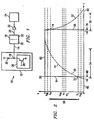
- FIGURE 1 illustrates a gate driver system 10 that includes a signal generator 12 which generates a slowly-slewing signal 14.
- a signal conditioner 16 couples to signal generator 12 at a node 18 to receive slowly-slewing signal 14, and produces rapidly-slewing signal 20 with minimal propagation delay.
- a gate driver 22 has an input coupled to signal 20 produced by signal conditioner 16, and an output coupled to a load 24. In general, signal conditioner 16 converts signal 14 into signal 20 to reduce the propagation delay from signal generator 12 to load 24.
- signal generator 12 may comprise a controller integrated circuit 26 (controller IC) having an output circuit 28, such as an NPN transistor, for generating signal 14.
- controller IC controller integrated circuit 26
- Signal generator 12 also contains a resistor 29 which couples to the collector terminal of the NPN transistor. Resistor 29 in combination with parasitic capacitances associated with the NPN transistor at node 18 limit the rise time of signal 14. The relatively slow operation of controller IC 26 also limits the fall time of signal 14. The propagation of signal 14 through slew-rate limited node 18 causes undesirably long propagation delays for system 10.
- Signal conditioner 16 includes a threshold circuit 30 and an output circuit 32.
- Threshold circuit 30 may comprise a network of comparators and memory devices that receive signal 14 and compare it with specified voltage thresholds to generate intermediate control signals.
- Output circuit 32 may comprise logic units that generate signal 20 in response to the intermediate control signals.
- Gate driver 22 comprises any suitable gate driver circuit that receives rapidly-slewing signal 20 and, in response, outputs a high voltage/high current signal to load 24.
- Load 24 comprises a power transistor, such as a metal-oxide semiconductor field effect transistor (MOSFET), a bipolar junction transistor (BJT), a silicon controlled rectifier (SCR), an insulated gate field effect transistor (IGFET), or other suitable load.
- MOSFET metal-oxide semiconductor field effect transistor
- BJT bipolar junction transistor
- SCR silicon controlled rectifier
- IGFET insulated gate field effect transistor
- the description of the present invention focuses primarily upon its operation with gate driver system 10, it should be understood that the present invention may operate with other applications that require rapid propagation of a slowly-slewing digital signal.
- the system of the present invention is described with reference to reducing the propagation delays of a voltage signal that is slew-rate limited due to capacitances, it may also operate to reduce the propagation delays of a current that is slew-rate limited due to inductances.
- the system of the present invention may reduce the propagation delay of any signal that experiences slew-rate limiting while carrying information through a mechanical, thermal, hydraulic, or pneumatic system.
- signal generator 12 In operation, signal generator 12 generates signal 14 having large rise and fall times.
- Signal conditioner 16 converts signal 14 into signal 20 by comparing signal 14 with a low voltage threshold V L and a high voltage threshold V H , wherein V H > V L .
- Signal conditioner 16 employs a memory device to determine whether signal 14 is rising or falling upon crossing either threshold V L or V H .
- Signal 20 exhibits small rise and fall times and minimal propagation delays.
- Gate driver 22 receives signal 20 and, in response, provides sufficient current to load 24 to slew its associated gate capacitance quickly. Supplying gate driver 22 with signal 20 reduces the overall propagation delay of system 10.
- FIGURE 2 illustrates signals 14 and 20 as a function of time.
- Signal 14 exhibits slow rising and falling edges 50 and 52, resulting in rise and fall times 54 and 56.
- Rise time 54 represents the time required for signal 14 to rise from near the low state supply voltage, such as 10% of the high state supply voltage, V 10 , to near the high state supply voltage, such as 90% of the high state supply voltage, V 90 .
- Fall time 56 represents the time required for signal 14 to fall from V 90 to V 10 .
- Signal conditioner 16 converts signal 14 into signal 20 by comparing signal 14 with voltage thresholds V L and V H , and by employing a memory device to determine whether signal 14 is rising or falling upon entering a voltage region 58.
- V L and V H define the inclusive boundaries of voltage region 58 between V L and V H .
- threshold circuit 30 of signal conditioner 18 receives signal 14 and compares signal 14 with voltage thresholds V L and V H .
- a memory flag is cleared when signal 14 crosses V L , and the memory flag is set when signal 14 crosses V H .
- Signal 14 is rising upon entering voltage region 58 if the memory flag is clear, and it is falling upon entering voltage region 58 if the memory flag is set.
- output circuit 32 When signal 14 is less than V L , output circuit 32 generates signal 20 with a low output state 60. When signal 14 enters region 58 and it is rising, as illustrated at 72, output circuit 32 generates signal 20 with a high output state 62 and the memory flag is cleared. While signal 14 is within voltage region 58 and the memory flag is clear, output circuit 32 generates signal 20 with high output state 62. When signal 14 is greater than V H , output circuit 32 generates signal 20 with high output state 62.
- output circuit 32 When signal 14 enters voltage region 58 and it is falling, as illustrated at 74, output circuit 32 generates signal 20 with low output state 60 and the memory flag is set. While signal 14 is within voltage region 58 and the memory flag is set, output circuit 32 generates signal 20 with low output state 60. Output states 60 and 62 may be adjusted to any two distinct desired reference voltages.
- Propagation delay 68 from rising edge 50 of signal 14 to rising edge 64 of signal 20 and propagation delay 70 from falling edge 52 of signal 14 to falling edge 66 of signal 20 are minimized by the proper selection of thresholds V L and V H .
- decreasing threshold V L may decrease propagation delay 68
- increasing threshold V H may decrease propagation delay 70.
- Voltage thresholds V H and V L are established to reduce delays 68 and 70 while simultaneously providing sufficient noise margins around reference voltages V and ground to determine the state of signal 14 accurately.
- FIGURE 2 illustrates V H lead than V 90 and V L greater than V 10 , the optimal choices for V H and V L may result in their being leas than, equal to, or greater than voltages V 90 and V 10 .
- System 10 also facilitates the passage of a digital signal having short-duration pulses through a slew-rate limited node. For example, if signal 14 rises from zero across V L and immediately thereafter falls below V L , then signal conditioner 16 generates signal 20 having high output state 62 followed by low output state 60. Similarly, if signal 14 falls from the high state supply voltage below V H and immediately thereafter rises above V H , then signal conditioner 16 generates signal 20 having low output state 60 followed by high output state 62.
- the successful transmission of signal 14 having short-duration pulses through slew-rate limited node 18 minimizes pulse skipping in a switch-mode converter containing a slew-rate limited node in the gate drive path.
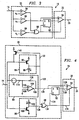
- FIGURE 3 illustrates one embodiment of signal conditioner 16 for propagating signal 14 through slew-rate limited node 18.
- Signal conditioner 16 includes threshold circuit 30 coupled to output circuit 32.
- Threshold circuit 30 includes a first voltage region comparator 84 associated with a high voltage threshold V H , a second voltage region comparator 86 associated with a low voltage threshold V L , and a logic unit 88 coupled to comparators 84 and 86.
- Threshold circuit 30 also includes a voltage threshold comparator 90 associated with an intermediate voltage threshold V T , and a memory device 92 coupled to logic unit 88 and comparator 90.
- Memory device 92 may comprise a flip-flop circuit having a data input terminal D, a clock input terminal C, and a complementary output terminal Q .
- comparator 90 has an intermediate high voltage threshold V TH and an intermediate low voltage threshold V TL , wherein V H > V TH > V T > V TL > V L . These additional voltage thresholds provide a noise margin around voltage threshold V T to determine the state of signals 14 and 20 accurately.
- Output circuit 32 includes a logic circuit 94 coupled to logic unit 88, comparator 90, and memory device 92.
- Logic circuit 94 may comprise a suitable configuration of logic elements that receives two input signals and a select signal and generates signal 20 equal to the first input signal when the select signal is high, and the second input signal when the select signal is low.
- comparators 84 and 86 determine whether signal 14 has entered voltage region 58.
- Comparator 90 simultaneously compares signal 14 with V T .
- a clocking signal triggers memory device 92 at clock input terminal C.
- memory device 92 records whether signal 14 is rising or falling upon entering voltage region 58 by determining whether signal 14 is above or below V T . In particular, if signal 14 is below V T upon entering voltage region 58, memory device 92 is cleared to indicate that signal 14 is rising. If signal 14 is above V T upon entering voltage region 58, memory device 92 is set to indicate that signal 14 is falling.
- Logic circuit 94 generates signal 20 having high state 62 when signal 14 is within voltage region 58 and memory device 92 is cleared, and when signal 14 is greater than V H .
- Logic circuit 94 generates signal 20 having low state 60 when signal 14 is within voltage region 58 and memory device 92 is set, and when signal 14 is less than V L .
- FIGURE 4 illustrates, in more detail, signal conditioner 16.
- comparatar 84 may comprise a comparator transistor 96, such as a p-channel MOSFET, having a gate terminal coupled to signal 14, a source terminal coupled to a reference voltage (V), a drain terminal coupled to a current source 98, and a threshold voltage equal to V H -V.
- Comparator 86 may comprise a comparator transistor 100, such as an n-channel MOSFET, having a gate terminal coupled to signal 14, a source terminal coupled to a reference voltage, such as ground, a drain terminal coupled to a current source 102, and a threshold voltage equal to V L .
- Logic unit 88 may comprise any suitable configuration of logic elements that perform an exclusive-or function upon two input signals.
- Comparator 90 may comprise a Schmitt trigger circuit, such as an operational amplifier 104 having an output terminal 106, a negative input terminal 108 coupled to a reference voltage, such as ground, and a positive input terminal 110 coupled to a reference voltage, such as intermediate voltage threshold V T , and signal 14 by a resistor 114, and output terminal 106 by a resistor 116.
- the value of resistor 114 in relation to the value of resistor 116 determines intermediate low voltage threshold, V TL , and intermediate high voltage threshold, V TH , at which Schmitt trigger circuit 90 will trigger.
- Voltage thresholds V TL and V TH provide a noise margin around voltage threshold V T to determine the state of signals 14 and 20 accurately.
- comparator 90 may comprise any Schmitt trigger circuit configuration that exhibits a suitable hysteresis.
- signal conditioner 16 receives signal 14 exhibiting rising and falling edges 50 and 52, rise time 54 and fall time 56. If rising edge 50 is less than V L , transistor 100 remains off and generates a logic signal 130 that is high. Simultaneously, transistor 96 turns on and generates a logic signal 132 that is also high. Logic unit 88 performs an exclusive-or logic function upon signals 130 and 132 to produce a voltage region signal 134 that is low. Schmitt trigger circuit 90 generates a voltage threshold signal 136 that is low in response to signal 14 being less than V TH . The flip-flop signal 138 of memory device 92 may be either high or low, depending upon the previous operation of signal conditioner 16.
- Logic circuit 94 received signals 134, 136, and 138 and generates signal 20 equal to signal 136 when the state of signal 134 is low, and signal 20 equal to signal 138 when the state of signal 134 is high. In this case, logic circuit 94 generates signal 20 equal to signal 136 that is low, in response to signal 134 that is low.
- transistor 100 turns on and generates logic signal 130 that is low. Simultaneously, transistor 96 remains on and generates logic signal 132 that is high.
- Logic unit 88 performs an exclusive-or logic function upon signals 130 and 132 to generate voltage region signal 134 that is high.
- Memory device 92 captures the state of signal 136 in response to a clocking signal at clock input terminal C, at the moment the state of signal 134 transitions from low to high. As a result, memory device 92 captures the low state of voltage threshold signal 136 and generates flip-flop signal 138 at complementary output terminal Q that is high.
- Logic circuit 94 receives signals 134, 136, and 138 and generates signal 20 equal to signal 138 that is high, in response to the high state of signal 134.
- Signal 20 exhibits a sharply rising edge 64. Since threshold V L may be set arbitrarily near ground, propagation delay 68 from the initiation of rising edge 50 to the initiation of rising edge 64 may be reduced to a very small value.
- Schmitt trigger circuit 90 As rising edge 50 of signal 14 passes voltage threshold V TH , Schmitt trigger circuit 90 generates signal 136 that is high.
- the noise margin between V T and V TH provides an accurate state determination for signal 14 despite potential oscillations of signal 14 around voltage threshold V T due to ambient noise.
- Transistor 100 remains on and generates signal 130 that is low while transistor 96 remains on and generates signal 132 that is high.
- Logic unit 88 performs an exclusive-or logic function upon signals 130 and 132 to generate signal 134 that is high.
- Memory device 92 generates signal 138 that is high.
- Logic circuit 94 receives signals 134, 136, and 138, and generates signal 20 equal to signal 138 that is high, in response to the high state of signal 134.
- transistor 100 As rising edge 50 of signal 14 passes voltage threshold V H , transistor 100 remains on and generates signal 130 that is low. Simultaneously, transistor 96 turns off and generates signal 132 that is low.
- Logic unit 88 performs an exclusive-or logic function upon signals 130 and 132 to generate signal 134 that is low.
- Memory device 92 generates signal 138 that is high.
- Schmitt trigger circuit 90 generates signal 136 that is high.
- Logic circuit 94 receives signals 134, 136, and 138 and generates a signal 20 equal to signal 136 that is high, in response to the low state of signal 134.
- Signal 20 remains high while rising edge 50 of signal 14 approaches voltage V and during falling edge 52 of signal 14 as it approaches voltage threshold V H from voltage V.
- transistor 100 As falling edge 52 of signal 14 passes voltage threshold V H , transistor 100 remains on and generates signal 130 that is low. Simultaneously, transistor 96 turns on and generated signal 132 that is high.
- Logic unit 88 performs an exclusive-or logic function upon signals 130 and 132 to generate signal 134 that is high.
- Memory device 92 captures the state of signal 136 in response to a clocking signal at clock input terminal C, at the moment the state of signal 134 transitions from low to high. As a result, memory device 92 captures the high state of signal 136 and generates signal 138 at complementary output terminal Q that is low.
- Logic circuit 94 receives signals 134, 136, and 138 and genemtoe signal 20 equal to signal 138 that is low, in response to the high state of signal 134.
- Signal 20 exhibits a sharply falling edge 66. Since threshold V H may be set arbitrarily near voltage V, propagation delay 70 from the initiation of falling edge 52 to the initiation of falling edge 66 may be reduced to a very small value.
- Schmitt trigger circuit 90 As falling edge 52 of signal 14 passes voltage threshold V TL , Schmitt trigger circuit 90 generates signal 136 that is low.
- the noise margin between V T and V TL provides an accurate state determination for signal 14 despite potential oscillations of signal 14 around voltage threshold V T due to ambient noise.
- Transistor 100 remains on and generated signal 130 that is low while transistor 96 remains on and generates signal 132 that is high.
- Logic unit 88 performs an exclusive-or logic function upon signals 130 and 132 to generate signal 134 that is high.
- Memory device 92 produces signal 138 that is low.
- Logic circuit 94 received signals 134, 136, and 138, and generates signal 20 equal to signal 138 that is low, in response to the high state of signal 134.
- transistor 100 turns off and generates signal 130 that is high. Simultaneously, transistor 96 remains on and generates signal 132 that is high.
- Logic unit 88 performs an exclusive-or logic function upon signals 130 and 132 to generate signal 134 that is low.
- Schmitt trigger circuit 90 generates signal 136 that is low, while memory device 92 generates signal 138 that is low.
- Logic circuit 94 receives signals 134, 136, and 138 and generates signal 20 equal to signal 136 that is low in response to the low state of signal 134.
- Signal 20 remains at a low state as falling edge 52 of signal 14 approaches ground, and, thereafter, while rising edge 50 of signal 14 again approaches voltage threshold V L .
- threshold circuit 30 further includes pull-up transistor 140, such as a p-channel MOSFET, having a source terminal coupled to a reference voltage V, a gate terminal coupled to the drain terminal of transistor 96, and a drain terminal coupled to signal 14.
- Transistor 140 provides an accurate state determination of signal 14 as slowly-rising edge 50 of signal 14 crosses voltage threshold V H .
- transistor 96 turns off and generated signal 132 that is low.
- transistor 140 turns on and "pulls up" input signal 14 to reference voltage V. This eliminates any potential oscillations of signal 14 around voltage threshold V H which may cause an inaccurate state determination of signals 14 and 20.
- an oscillation of rising edge 50 of signal 14 around voltage threshold V H may cause a glitch in output signal 20.
- signal conditioner 16 may generate signal 20 that is low and immediately thereafter generate signal 20 that is high.
- the added transistor 140 pulls signal 14 to a high state after rising edge 50 of signal 14 crosses voltage threshold V H . This reduces the effects of any potential oscillations of signal 14 due to noise and produces an accurate state determination for both signals 14 and 20.
- Threshold circuit 30 may similarly include a pull-down transistor that eliminates any potential oscillations of signal 14 around voltage threshold V L .
- FIGURE 5 illustrates another embodiment of signal conditioner 16.
- comparator 84 includes a Schmitt trigger circuit, such as an operational amplifier 150 having an output terminal 152, a negative input terminal 154 coupled to a reference voltage, such as voltage threshold V H , and signal 14, and a positive input terminal 156 coupled to a reference voltage, such as ground, by a resistor 158, and output terminal 152 by a resistor 160.
- the value of resistor 158 in relation to the value of resistor 160 determines a high plus voltage threshold V H+ , and a high minus voltage threshold V H- , at which Schmitt trigger circuit 84 will trigger.
- Schmitt trigger circuit 84 triggers from a high state, to a low state when a rising signal 14 crosses high plus voltage threshold V H+ , and triggers from a low state to a high state when a falling signal 14 crosses high minus voltage threshold V H- , wherein V H+ > V H > V H- .
- Comparator 86 includes a Schmitt trigger circuit, such as an operational amplifier 162 having an output terminal 164, a negative input terminal 166 coupled to a reference voltage, such as voltage threshold V L , and signal 14, and a positive input terminal 168 coupled to a reference voltage, such as ground, by a resistor 170, and output terminal 164 by a resistor 172.
- the value of resistor 170 in relation to the value of resistor 172 determines a low plus voltage threshold V L+ , and a low minus voltage threshold V L- , at which Schmitt trigger circuit 86 will trigger.
- Schmitt trigger circuit 86 triggers from a high state to a low state when a rising signal 14 crosses low plus voltage threshold V L+ , and triggers from a low state to a high state when a falling signal 14 crosses low minus voltage threshold V L- , wherein V L+ > V L > V L- .
- Adding hysteresis to thresholds V L and V H prevents noise within signal 14 from causing spurious transitions in signal 20 around voltage thresholds V L and V H .
- comparators 84 and 86 may comprise any Schmitt trigger circuit configurations that exhibit a suitable hysteresis.
- comparators 84 and 86 may both comprise noninverting Schmitt trigger circuits or may both comprise inverting Schmitt trigger circuits.
Landscapes
- Physics & Mathematics (AREA)
- Nonlinear Science (AREA)
- Manipulation Of Pulses (AREA)
- Logic Circuits (AREA)
Applications Claiming Priority (2)
| Application Number | Priority Date | Filing Date | Title |
|---|---|---|---|
| US7060898P | 1998-01-06 | 1998-01-06 | |
| US70608 | 1998-01-06 |
Publications (2)
| Publication Number | Publication Date |
|---|---|
| EP0928066A1 true EP0928066A1 (de) | 1999-07-07 |
| EP0928066B1 EP0928066B1 (de) | 2004-10-06 |
Family
ID=22096346
Family Applications (1)
| Application Number | Title | Priority Date | Filing Date |
|---|---|---|---|
| EP99200001A Expired - Lifetime EP0928066B1 (de) | 1998-01-06 | 1999-01-05 | Schaltung zum Steilermachen von Pulsflanken |
Country Status (4)
| Country | Link |
|---|---|
| US (1) | US6275074B1 (de) |
| EP (1) | EP0928066B1 (de) |
| JP (1) | JP4008612B2 (de) |
| DE (1) | DE69920780T2 (de) |
Families Citing this family (8)
| Publication number | Priority date | Publication date | Assignee | Title |
|---|---|---|---|---|
| US7130340B1 (en) * | 2000-10-27 | 2006-10-31 | Sun Microsystems, Inc. | Noise margin self-diagnostic receiver logic |
| KR100606144B1 (ko) * | 2002-03-06 | 2006-08-01 | 산켄덴키 가부시키가이샤 | 교류신호의 레벨검출회로 |
| KR100449950B1 (ko) * | 2002-07-19 | 2004-09-30 | 주식회사 하이닉스반도체 | 부하구동력 가변형 증폭회로 |
| JP4546716B2 (ja) * | 2003-11-10 | 2010-09-15 | シャープ株式会社 | Pllクロック信号生成回路 |
| KR100616218B1 (ko) * | 2004-07-19 | 2006-08-25 | 매그나칩 반도체 유한회사 | 출력신호의 슬루율을 제어할 수 있는 연산증폭기 |
| KR100845773B1 (ko) * | 2006-08-11 | 2008-07-14 | 주식회사 하이닉스반도체 | 반도체 메모리 장치의 파워 업 신호 트립 포인트 측정 회로 및 이를 이용한 파워 업 신호 트립 포인트 레벨 측정 방법 |
| JP6133709B2 (ja) * | 2013-06-25 | 2017-05-24 | ローム株式会社 | 差動レシーバ、それを用いた電子機器、産業機器ならびに差動信号の受信方法 |
| KR102812457B1 (ko) * | 2020-07-27 | 2025-05-26 | 삼성전자주식회사 | 스턱을 검출하는 전자 장치 및 스턱을 모니터하는 방법 |
Citations (4)
| Publication number | Priority date | Publication date | Assignee | Title |
|---|---|---|---|---|
| DE3837821A1 (de) * | 1988-11-08 | 1990-05-10 | Asea Brown Boveri | Cmos-praezisions-schmitt-trigger |
| US5097147A (en) * | 1991-02-01 | 1992-03-17 | Tektronix, Inc. | Limited amplitude signal trigger circuit |
| US5278462A (en) * | 1992-04-24 | 1994-01-11 | Fasco Controls Corporation | Threshold crossover detector with improved digital noise rejection |
| US5324995A (en) * | 1992-11-06 | 1994-06-28 | National Semiconductor Corporation | Sample and hold voltage receiver having reduced harmonic distortion |
Family Cites Families (9)
| Publication number | Priority date | Publication date | Assignee | Title |
|---|---|---|---|---|
| ZA805412B (en) * | 1979-09-14 | 1981-08-26 | Plessey Overseas | Zero-crossing comparators with threshold validation |
| US4421995A (en) * | 1981-07-30 | 1983-12-20 | The United States Of America As Represented By The United States Department Of Energy | Timing discriminator using leading-edge extrapolation |
| DE4231611A1 (de) * | 1992-09-22 | 1994-03-24 | Thomson Brandt Gmbh | Verfahren und Vorrichtung zur Überwachung eines alternierenden Signals |
| US5554948A (en) * | 1994-05-31 | 1996-09-10 | Delco Electronics Corporation | Adaptive threshold circuit with deceleration compensation |
| CA2134310A1 (en) * | 1994-10-25 | 1996-04-26 | Telemus Inc. | Wideband digital peak detector |
| DE69529331T2 (de) * | 1995-01-31 | 2003-10-23 | Stmicroelectronics S.R.L., Agrate Brianza | Treiberschaltung mit Ladungspumpe für einen Leistungstransistor |
| US5532626A (en) * | 1995-02-06 | 1996-07-02 | Unitrode Corporation | Off-line controller having a line voltage detector and a switched current bootstrap circuit |
| JPH1093641A (ja) * | 1996-09-12 | 1998-04-10 | Nec Corp | 多値fsk復調ウィンドウコンパレータ |
| US6100678A (en) * | 1999-08-26 | 2000-08-08 | Linear Technology Corporation | Single package pin providing soft-start and short-circuit timer functions in a voltage regulator controller |
-
1999
- 1999-01-04 US US09/225,100 patent/US6275074B1/en not_active Expired - Lifetime
- 1999-01-05 EP EP99200001A patent/EP0928066B1/de not_active Expired - Lifetime
- 1999-01-05 DE DE69920780T patent/DE69920780T2/de not_active Expired - Lifetime
- 1999-01-06 JP JP03764599A patent/JP4008612B2/ja not_active Expired - Fee Related
Patent Citations (4)
| Publication number | Priority date | Publication date | Assignee | Title |
|---|---|---|---|---|
| DE3837821A1 (de) * | 1988-11-08 | 1990-05-10 | Asea Brown Boveri | Cmos-praezisions-schmitt-trigger |
| US5097147A (en) * | 1991-02-01 | 1992-03-17 | Tektronix, Inc. | Limited amplitude signal trigger circuit |
| US5278462A (en) * | 1992-04-24 | 1994-01-11 | Fasco Controls Corporation | Threshold crossover detector with improved digital noise rejection |
| US5324995A (en) * | 1992-11-06 | 1994-06-28 | National Semiconductor Corporation | Sample and hold voltage receiver having reduced harmonic distortion |
Also Published As
| Publication number | Publication date |
|---|---|
| DE69920780T2 (de) | 2005-11-24 |
| DE69920780D1 (de) | 2004-11-11 |
| JP4008612B2 (ja) | 2007-11-14 |
| JP2000188532A (ja) | 2000-07-04 |
| EP0928066B1 (de) | 2004-10-06 |
| US6275074B1 (en) | 2001-08-14 |
Similar Documents
| Publication | Publication Date | Title |
|---|---|---|
| US4825101A (en) | Full-level, fast CMOS output buffer | |
| US4972101A (en) | Noise reduction in CMOS driver using capacitor discharge to generate a control voltage | |
| US6337647B1 (en) | Digital-analog current converter | |
| US6181178B1 (en) | Systems and methods for correcting duty cycle deviations in clock and data signals | |
| US6664805B2 (en) | Switched capacitor piecewise linear slew rate control methods for output devices | |
| CN116918257A (zh) | 集成总线接口下降和上升时间加速器方法 | |
| US5808481A (en) | Output swing clamp for USB differential buffer | |
| EP0503803A1 (de) | Schaltkreis | |
| JPH04229714A (ja) | バッファを有する集積回路 | |
| US6275074B1 (en) | System for propagating a digital signal through a slew-rate limited node and method of operation | |
| US20110025395A1 (en) | System and method for compensating pulse generator for process and temperature variations | |
| KR100686252B1 (ko) | 스위칭 잡음을 감소시키는 회로 | |
| US5489859A (en) | CMOS output circuit with high speed high impedance mode | |
| EP0642226A2 (de) | Umsetzungsschaltungen mit symmetrischen Schaltverzögerungen | |
| US6281708B1 (en) | Tri-state bus amplifier-accelerator | |
| US20070182461A1 (en) | Resonant line drivers | |
| JPH0514167A (ja) | 出力ドライバ回路 | |
| KR20000075565A (ko) | 출력단 | |
| JP4576717B2 (ja) | コンパレータ回路 | |
| US6177818B1 (en) | Complementary depletion switch body stack off-chip driver | |
| US4554464A (en) | Propagation delay generator | |
| JP3654484B2 (ja) | 出力バッファ回路 | |
| JP2577425B2 (ja) | 駆動回路 | |
| US7002392B2 (en) | Converting signals from a low voltage domain to a high voltage domain | |
| EP0712205A2 (de) | Zeitschaltung mit festem Intervall |
Legal Events
| Date | Code | Title | Description |
|---|---|---|---|
| PUAI | Public reference made under article 153(3) epc to a published international application that has entered the european phase |
Free format text: ORIGINAL CODE: 0009012 |
|
| AK | Designated contracting states |
Kind code of ref document: A1 Designated state(s): DE FR GB IT NL |
|
| AX | Request for extension of the european patent |
Free format text: AL;LT;LV;MK;RO;SI |
|
| 17P | Request for examination filed |
Effective date: 20000107 |
|
| AKX | Designation fees paid |
Free format text: DE FR GB IT NL |
|
| 17Q | First examination report despatched |
Effective date: 20021009 |
|
| GRAP | Despatch of communication of intention to grant a patent |
Free format text: ORIGINAL CODE: EPIDOSNIGR1 |
|
| GRAS | Grant fee paid |
Free format text: ORIGINAL CODE: EPIDOSNIGR3 |
|
| GRAA | (expected) grant |
Free format text: ORIGINAL CODE: 0009210 |
|
| AK | Designated contracting states |
Kind code of ref document: B1 Designated state(s): DE FR GB IT NL |
|
| PG25 | Lapsed in a contracting state [announced via postgrant information from national office to epo] |
Ref country code: NL Free format text: LAPSE BECAUSE OF FAILURE TO SUBMIT A TRANSLATION OF THE DESCRIPTION OR TO PAY THE FEE WITHIN THE PRESCRIBED TIME-LIMIT Effective date: 20041006 Ref country code: IT Free format text: LAPSE BECAUSE OF FAILURE TO SUBMIT A TRANSLATION OF THE DESCRIPTION OR TO PAY THE FEE WITHIN THE PRESCRIBED TIME-LIMIT;WARNING: LAPSES OF ITALIAN PATENTS WITH EFFECTIVE DATE BEFORE 2007 MAY HAVE OCCURRED AT ANY TIME BEFORE 2007. THE CORRECT EFFECTIVE DATE MAY BE DIFFERENT FROM THE ONE RECORDED. Effective date: 20041006 |
|
| REG | Reference to a national code |
Ref country code: GB Ref legal event code: FG4D |
|
| REF | Corresponds to: |
Ref document number: 69920780 Country of ref document: DE Date of ref document: 20041111 Kind code of ref document: P |
|
| NLV1 | Nl: lapsed or annulled due to failure to fulfill the requirements of art. 29p and 29m of the patents act | ||
| ET | Fr: translation filed | ||
| PLBE | No opposition filed within time limit |
Free format text: ORIGINAL CODE: 0009261 |
|
| STAA | Information on the status of an ep patent application or granted ep patent |
Free format text: STATUS: NO OPPOSITION FILED WITHIN TIME LIMIT |
|
| 26N | No opposition filed |
Effective date: 20050707 |
|
| PGFP | Annual fee paid to national office [announced via postgrant information from national office to epo] |
Ref country code: GB Payment date: 20131227 Year of fee payment: 16 |
|
| PGFP | Annual fee paid to national office [announced via postgrant information from national office to epo] |
Ref country code: DE Payment date: 20140131 Year of fee payment: 16 |
|
| PGFP | Annual fee paid to national office [announced via postgrant information from national office to epo] |
Ref country code: FR Payment date: 20131223 Year of fee payment: 16 |
|
| REG | Reference to a national code |
Ref country code: DE Ref legal event code: R119 Ref document number: 69920780 Country of ref document: DE |
|
| GBPC | Gb: european patent ceased through non-payment of renewal fee |
Effective date: 20150105 |
|
| PG25 | Lapsed in a contracting state [announced via postgrant information from national office to epo] |
Ref country code: GB Free format text: LAPSE BECAUSE OF NON-PAYMENT OF DUE FEES Effective date: 20150105 Ref country code: DE Free format text: LAPSE BECAUSE OF NON-PAYMENT OF DUE FEES Effective date: 20150801 |
|
| REG | Reference to a national code |
Ref country code: FR Ref legal event code: ST Effective date: 20150930 |
|
| PG25 | Lapsed in a contracting state [announced via postgrant information from national office to epo] |
Ref country code: FR Free format text: LAPSE BECAUSE OF NON-PAYMENT OF DUE FEES Effective date: 20150202 |