EP0928068A1 - TTL-CMOS Eingangspufferstufe mit geringem Leistungsverbrauch - Google Patents
TTL-CMOS Eingangspufferstufe mit geringem Leistungsverbrauch Download PDFInfo
- Publication number
- EP0928068A1 EP0928068A1 EP97830743A EP97830743A EP0928068A1 EP 0928068 A1 EP0928068 A1 EP 0928068A1 EP 97830743 A EP97830743 A EP 97830743A EP 97830743 A EP97830743 A EP 97830743A EP 0928068 A1 EP0928068 A1 EP 0928068A1
- Authority
- EP
- European Patent Office
- Prior art keywords
- buffer stage
- transistors
- ttl
- stage according
- inverter
- Prior art date
- Legal status (The legal status is an assumption and is not a legal conclusion. Google has not performed a legal analysis and makes no representation as to the accuracy of the status listed.)
- Withdrawn
Links
Images


Classifications
-
- H—ELECTRICITY
- H03—ELECTRONIC CIRCUITRY
- H03K—PULSE TECHNIQUE
- H03K19/00—Logic circuits, i.e. having at least two inputs acting on one output; Inverting circuits
- H03K19/0008—Arrangements for reducing power consumption
- H03K19/0016—Arrangements for reducing power consumption by using a control or a clock signal, e.g. in order to apply power supply
Definitions
- This invention relates to a novel configuration of an input buffer which is capable of effecting conversions between TTL and CMOS logic levels, while complying with low supply consumption specifications.
- the invention relates to a low-consumption TTL-CMOS input buffer stage of the type which comprises a chain of inverters cascade connected between an input, receiving electric signals at a TTL logic level, and an output reproducing electric signals at a CMOS logic level, the inverters being powered between a first or supply voltage reference and a second or ground reference.
- the input buffer stage is asked to effect a conversion of logic levels.
- the internal circuitry will receive signals which are purely CMOS but logically congruous with the TTL inputs of the integrated circuit.
- an input signal is regarded to have a "low” logic value if the signal amplitude is less than 0.8V, and to have a "high” logic value if the signal amplitude exceeds 2.0V.
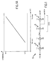
- the accompanying Figure 1 shows a circuit diagram of a conventional input buffer stage 1 for TTL-CMOS conversion, in its simplest form.
- the buffer 1 is basically formed by a chain of inverters which are all supplied by same device internal supply voltage Vcc.
- the changeover threshold of the circuit 1 in Figure 1 increases linearly with the supply voltage Vcc. Furthermore, the threshold sweep, for a sweep ⁇ of the voltage V, is bound to be ⁇ /2 regardless of the aspect ratii of the inverters in the chain.
- NM H 2.0 - V Th (Vcc) and, therefore, minimal while Vcc is at a maximum.
- a typical static consumption of tens of microAmperes has been found for a single buffer. This consumption is unacceptable, especially in circuits that are to be incorporated to low-power amplifiers which often require that, following a time latency of the inputs, the circuit goes to a standby state of low consumption and be prepared for a new switching.
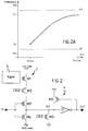
- FIG. 2 Shown schematically in Figure 2 is an input buffer stage 5 which is again configured as an inverter chain and includes a current generator 6 for controlling the switching threshold in a high supply voltage situation.
- the first inverter 7 in the chain is supplied the voltage Vcc through a PMOS transistor M1 connected to the current generator 6. Since the current through the first inverter 7 is limited by M1, especially at high supply voltages, the rise in the switching threshold will be reduced even as Vcc increases. Thus, the margin for noise is improved in the circuit 5.
- the underlying technical problem of this invention is to provide a novel structure of a TTL-CMOS input buffer stage which has such constructional and functional features as to ensure lower consumption than the solutions proposed by the prior art.
- the principle behind this invention is that of having the first inverter in the buffer sized symmetrically with its the pull-up and pull-down portions, and further providing two signal paths, one for normal operation and the other for low-consumption operation.
- TTL-CMOS input buffer stage according to this invention which is intended for conversion between TTL and CMOS logic levels, as well as to comply with specifications of power supply low-consumption.
- the stage 10 comprises essentially a chain of cascade connected inverters.
- the chain is made up of four cascaded inverters, as respectively indicated at 11, 12, 13 and 14, an input APAD at a TTL logic level, and an output ADD at a CMOS logic level.
- An inverted output signal ADD_N is picked up between the third and fourth inverters, 13 and 14.
- the first inverter 11 of the chain has a peculiar structure in the stage 10 of this invention.
- the first inverter 11 comprises a PMOS switch MP1 and an NMOS transistor MN1 which are connected in series with each other between a first or supply voltage reference Vcc and a second or ground reference GND.
- the gate terminal of the PMOS transistor MP1 receives a control signal LOWPOWER, while the gate terminal of the NMOS transistor MN1 receives the same signal in its negated form, LOWPOWER_N.
- an inverter 15 formed of a complementary pair of high voltage transistors PH1 and NH1.
- the gate terminals of these transistors PH1, NH1 are connected together at the common input terminal APAD.
- the transistor NH1 has respective source and body terminals connected toward to the Y node and the n-well region to the voltage supply Vcc.
- the node K interconnecting the transistors PH1 and NH1 is connected to the input of the second inverter 12 in the chain that includes the buffer 10.
- the two PMOS transistors MP1 and PH1 -- which are located in the switch portion of the inverter 11 -- are interconnected at a node X.
- the body terminal of the transistor PH1 is connected to the node X.
- the node X is connected to the voltage supply Vcc through a parallel of:
- the node X is connected to ground through a capacitor C1.
- the two NMOS transistors MN1 and NH1 -- which are located in the switch portion of the inverter 11, relative to the node K -- are interconnected at a node Y.
- the node Y is connected to the ground GND through a parallel of:
- the transistors that comprise the first inverter 11 are formed in separate wells from the other inverters in the chain.
- the input inverter 11 is connected to the ground GND and the voltage supply Vcc through two circuit networks, as shown in Figures 4 and 5, which act alternatively to each other according to the operating mode of the device.
- the first of these circuit networks i.e. the network which is active during normal operation of the stage 10, is drawn in heavier lines in Figure 4.
- the second circuit network is also drawn in heavier lines which is active while the stage 10 is operated in a condition of low consumption.
- the transistors MP2 and MN2 less conductive.
- the crowbar current flowing through the first TTL inverter 11 in the chain of the input buffer 10 can be limited by suitably selecting which of the supply paths is to be connected to the stage 10.
- the operating mode is selected by means of the activation signal LOWPOWER, which will be generated internally of the host integrated circuit of the input stage 10.
- MP1 and MH1 are on and receive a TTL input.
- the signal LOWPOWER is suitably generated upon a predetermined latency period, e.g. 300nsec, of the inputs being exceeded.
- the buffer 10 is still able to switch over while being operated in the low-consumption mode; and it is the very switching of the buffer that will cause the device to be restored to normal operation, by zeroing the signal LOWPOWER.
- the inventive solution maintains the input buffers 10 operative even while in the low-consumption mode of operation.
- capacitors C1 and C2 associated with the diode-connected low-threshold native transistors, D1 and D2, form parts of the low-consumption bias network shown in Figure 5.
- the transistors MP2 and MN2 would be unable to provide by themselves the current required for a correct buffer output.
- the transistors MP2 and MN2 have been selected intentionally resistive in order to limit the crowbar current, but their resistivity would effectively prevent any subsequent switchings of the buffer before the signal LOWPOWER goes to a zero logic value.
- capacitors C1 and C2 have been included to act as charge stores, in case the transition of LOWPOWER is slower than expected due to ill-estimated internal delays.
- the native diodes D1 and D2 which are strongly conductive and normally in the 'off' state, are effective to prevent the capacitor C1 from becoming discharged and the capacitor C2 from becoming charged above a given limit, even if no transition of LOWPOWER ever occurs.
- the components C1, C2, D1 and D2 while not being strictly necessary, still ensure improved operability of the buffer 10, even in the unfortunate event of the circuit being unable to exit the low consumption condition due to errors in the internal logic network that generates the signal LOWPOWER.
- the specifications for low consumption operation are usually quite stringent dissipation-wise. It is expected that the signal LOWPOWER de-activates most of the circuitry of the CMOS integrated circuit. By actually attenuating the internal noise produced on the power supply and the ground, the integrated circuit would be affected by less noise.
- the inventive circuit could be modified, as regards the normal operation mode, to have the gate of the PMOS transistor MP1 powered from a bias network incorporating a current generator 16.
- This may be a welcome modification in that it affords improved flexibility for the normal or high-consumption operation mode.
- the input buffer stage of this invention does solve the technical problem, and affords a number of advantages, outstanding among which is that a TTL-CMOS input buffer can be provided which has variable consumption features.
- This buffer can be useful with all those CMOS circuit structures which require TTL-CMOS conversion, and wherein problems of low static consumption of the inputs from the supply are encountered.
Landscapes
- Physics & Mathematics (AREA)
- Engineering & Computer Science (AREA)
- Computer Hardware Design (AREA)
- Computing Systems (AREA)
- General Engineering & Computer Science (AREA)
- Mathematical Physics (AREA)
- Logic Circuits (AREA)
Priority Applications (2)
| Application Number | Priority Date | Filing Date | Title |
|---|---|---|---|
| EP97830743A EP0928068A1 (de) | 1997-12-31 | 1997-12-31 | TTL-CMOS Eingangspufferstufe mit geringem Leistungsverbrauch |
| US09/231,130 US6307396B1 (en) | 1997-12-31 | 1998-12-30 | Low-consumption TTL-CMOS input buffer stage |
Applications Claiming Priority (1)
| Application Number | Priority Date | Filing Date | Title |
|---|---|---|---|
| EP97830743A EP0928068A1 (de) | 1997-12-31 | 1997-12-31 | TTL-CMOS Eingangspufferstufe mit geringem Leistungsverbrauch |
Publications (1)
| Publication Number | Publication Date |
|---|---|
| EP0928068A1 true EP0928068A1 (de) | 1999-07-07 |
Family
ID=8230942
Family Applications (1)
| Application Number | Title | Priority Date | Filing Date |
|---|---|---|---|
| EP97830743A Withdrawn EP0928068A1 (de) | 1997-12-31 | 1997-12-31 | TTL-CMOS Eingangspufferstufe mit geringem Leistungsverbrauch |
Country Status (2)
| Country | Link |
|---|---|
| US (1) | US6307396B1 (de) |
| EP (1) | EP0928068A1 (de) |
Cited By (1)
| Publication number | Priority date | Publication date | Assignee | Title |
|---|---|---|---|---|
| EP1064726A1 (de) * | 1998-03-16 | 2001-01-03 | Infineon Technologies AG | Schaltungsanordnung zur reduzierung des leckstromes |
Families Citing this family (8)
| Publication number | Priority date | Publication date | Assignee | Title |
|---|---|---|---|---|
| JP2002197867A (ja) * | 2000-12-28 | 2002-07-12 | Nec Corp | 半導体装置 |
| US7214945B2 (en) * | 2002-06-11 | 2007-05-08 | Canon Kabushiki Kaisha | Radiation detecting apparatus, manufacturing method therefor, and radiation image pickup system |
| US7170327B2 (en) * | 2003-06-27 | 2007-01-30 | Intel Corporation | System and method for data retention with reduced leakage current |
| KR100687867B1 (ko) * | 2004-07-21 | 2007-02-27 | 주식회사 하이닉스반도체 | 저전력 고성능 인버터 회로 |
| US7852113B2 (en) * | 2005-08-16 | 2010-12-14 | Novelics, Llc. | Leakage control |
| TWI654842B (zh) * | 2017-10-20 | 2019-03-21 | 立積電子股份有限公司 | 反相器 |
| US10461749B1 (en) * | 2018-10-25 | 2019-10-29 | Shenzhen GOODIX Technology Co., Ltd. | Ground intermediation for inter-domain buffer stages |
| US10812081B1 (en) * | 2019-09-27 | 2020-10-20 | Apple Inc. | Output signal control during retention mode operation |
Citations (7)
| Publication number | Priority date | Publication date | Assignee | Title |
|---|---|---|---|---|
| US4437024A (en) * | 1981-10-22 | 1984-03-13 | Rca Corporation | Actively controlled input buffer |
| US5151620A (en) * | 1991-03-25 | 1992-09-29 | Industrial Technology Research Institute | CMOS input buffer with low power consumption |
| JPH05304464A (ja) * | 1992-04-27 | 1993-11-16 | Nec Ic Microcomput Syst Ltd | 入力バッファ回路 |
| EP0595318A2 (de) * | 1992-10-30 | 1994-05-04 | Nec Corporation | Pufferschaltung für Eingangsignale mit geringerer Amplitude als die Speisespannung |
| EP0621694A2 (de) * | 1993-04-20 | 1994-10-26 | International Business Machines Corporation | Schnittstellenschaltung mit niedrigem Verbrauch |
| JPH08138381A (ja) * | 1994-11-07 | 1996-05-31 | Mitsubishi Electric Corp | 半導体集積回路装置およびその製造方法および内部電圧発生回路 |
| US5614847A (en) * | 1992-04-14 | 1997-03-25 | Hitachi, Ltd. | Semiconductor integrated circuit device having power reduction mechanism |
Family Cites Families (5)
| Publication number | Priority date | Publication date | Assignee | Title |
|---|---|---|---|---|
| US4469959A (en) * | 1982-03-15 | 1984-09-04 | Motorola, Inc. | Input buffer |
| US4642488A (en) * | 1985-09-03 | 1987-02-10 | Codex Corporation | CMOS input buffer accepting TTL level inputs |
| KR910005609B1 (ko) * | 1988-07-19 | 1991-07-31 | 삼성전자 주식회사 | 복수전압 ic용 입력신호 로직 판별회로 |
| US5144167A (en) * | 1991-05-10 | 1992-09-01 | Altera Corporation | Zero power, high impedance TTL-to-CMOS converter |
| US5341046A (en) * | 1992-12-07 | 1994-08-23 | Ncr Corporation | Threshold controlled input circuit for an integrated circuit |
-
1997
- 1997-12-31 EP EP97830743A patent/EP0928068A1/de not_active Withdrawn
-
1998
- 1998-12-30 US US09/231,130 patent/US6307396B1/en not_active Expired - Fee Related
Patent Citations (7)
| Publication number | Priority date | Publication date | Assignee | Title |
|---|---|---|---|---|
| US4437024A (en) * | 1981-10-22 | 1984-03-13 | Rca Corporation | Actively controlled input buffer |
| US5151620A (en) * | 1991-03-25 | 1992-09-29 | Industrial Technology Research Institute | CMOS input buffer with low power consumption |
| US5614847A (en) * | 1992-04-14 | 1997-03-25 | Hitachi, Ltd. | Semiconductor integrated circuit device having power reduction mechanism |
| JPH05304464A (ja) * | 1992-04-27 | 1993-11-16 | Nec Ic Microcomput Syst Ltd | 入力バッファ回路 |
| EP0595318A2 (de) * | 1992-10-30 | 1994-05-04 | Nec Corporation | Pufferschaltung für Eingangsignale mit geringerer Amplitude als die Speisespannung |
| EP0621694A2 (de) * | 1993-04-20 | 1994-10-26 | International Business Machines Corporation | Schnittstellenschaltung mit niedrigem Verbrauch |
| JPH08138381A (ja) * | 1994-11-07 | 1996-05-31 | Mitsubishi Electric Corp | 半導体集積回路装置およびその製造方法および内部電圧発生回路 |
Non-Patent Citations (1)
| Title |
|---|
| PATENT ABSTRACTS OF JAPAN vol. 018, no. 105 (E - 1512) 21 February 1994 (1994-02-21) * |
Cited By (1)
| Publication number | Priority date | Publication date | Assignee | Title |
|---|---|---|---|---|
| EP1064726A1 (de) * | 1998-03-16 | 2001-01-03 | Infineon Technologies AG | Schaltungsanordnung zur reduzierung des leckstromes |
Also Published As
| Publication number | Publication date |
|---|---|
| US6307396B1 (en) | 2001-10-23 |
Similar Documents
| Publication | Publication Date | Title |
|---|---|---|
| US6359493B2 (en) | Level shift circuit | |
| US5969542A (en) | High speed gate oxide protected level shifter | |
| US5872464A (en) | Input buffer with stabilized trip points | |
| US7196547B2 (en) | Level shifter and buffer circuit | |
| EP0774838B1 (de) | CMOS-Schnittstellenschaltung zum Ankoppeln einer integrierten Schaltung mit niedriger Versorgungsspannung an Vorrichtungen mit einer höheren Versorgungsspannung | |
| WO1997029544A1 (en) | Gate oxide voltage limiting devices for digital circuits | |
| JPH0338873A (ja) | 集積回路 | |
| US5929679A (en) | Voltage monitoring circuit capable of reducing power dissipation | |
| EP0502597A2 (de) | CMOS-Ausgangspufferschaltung | |
| US6249146B1 (en) | MOS output buffer with overvoltage protection circuitry | |
| US6307396B1 (en) | Low-consumption TTL-CMOS input buffer stage | |
| JPS58123223A (ja) | Mosパワ−オンリセツト回路 | |
| US7088167B2 (en) | Level conversion for use in semiconductor device | |
| US20060097769A1 (en) | Level shift circuit and semiconductor circuit device including the level shift circuit | |
| US6265931B1 (en) | Voltage reference source for an overvoltage-tolerant bus interface | |
| JPH1196749A (ja) | 電圧レベル変換回路 | |
| US7208978B2 (en) | Semiconductor device | |
| US5905399A (en) | CMOS integrated circuit regulator for reducing power supply noise | |
| US6084431A (en) | Output circuit providing protection against external voltages in excess of power-supply voltage | |
| JPH04329023A (ja) | 出力バッファ回路 | |
| US5345111A (en) | High-speed current sense amplifier | |
| US5767696A (en) | Tri-state devices having exclusive gate output control | |
| US6271707B1 (en) | Level shifter | |
| JP3437578B2 (ja) | 過渡的な同時導通を低減するための回路 | |
| CN117691986A (zh) | 一种高速双电平转换器 |
Legal Events
| Date | Code | Title | Description |
|---|---|---|---|
| PUAI | Public reference made under article 153(3) epc to a published international application that has entered the european phase |
Free format text: ORIGINAL CODE: 0009012 |
|
| AK | Designated contracting states |
Kind code of ref document: A1 Designated state(s): DE FR GB IT |
|
| AX | Request for extension of the european patent |
Free format text: AL;LT;LV;MK;RO;SI |
|
| 17P | Request for examination filed |
Effective date: 19991007 |
|
| AKX | Designation fees paid |
Free format text: DE FR GB IT |
|
| 17Q | First examination report despatched |
Effective date: 20020206 |
|
| STAA | Information on the status of an ep patent application or granted ep patent |
Free format text: STATUS: THE APPLICATION HAS BEEN WITHDRAWN |
|
| 18W | Application withdrawn |
Effective date: 20041109 |