EP0928638A2 - Verfahren zum Beschichten eines Substrates und Vorrichtung zum Beschichten und Härten der Beschichtung - Google Patents
Verfahren zum Beschichten eines Substrates und Vorrichtung zum Beschichten und Härten der Beschichtung Download PDFInfo
- Publication number
- EP0928638A2 EP0928638A2 EP98310263A EP98310263A EP0928638A2 EP 0928638 A2 EP0928638 A2 EP 0928638A2 EP 98310263 A EP98310263 A EP 98310263A EP 98310263 A EP98310263 A EP 98310263A EP 0928638 A2 EP0928638 A2 EP 0928638A2
- Authority
- EP
- European Patent Office
- Prior art keywords
- solvent
- film
- substrate
- gas
- coating
- Prior art date
- Legal status (The legal status is an assumption and is not a legal conclusion. Google has not performed a legal analysis and makes no representation as to the accuracy of the status listed.)
- Withdrawn
Links
Images














Classifications
-
- B—PERFORMING OPERATIONS; TRANSPORTING
- B05—SPRAYING OR ATOMISING IN GENERAL; APPLYING FLUENT MATERIALS TO SURFACES, IN GENERAL
- B05C—APPARATUS FOR APPLYING FLUENT MATERIALS TO SURFACES, IN GENERAL
- B05C5/00—Apparatus in which liquid or other fluent material is projected, poured or allowed to flow on to the surface of the work
-
- H—ELECTRICITY
- H10—SEMICONDUCTOR DEVICES; ELECTRIC SOLID-STATE DEVICES NOT OTHERWISE PROVIDED FOR
- H10P—GENERIC PROCESSES OR APPARATUS FOR THE MANUFACTURE OR TREATMENT OF DEVICES COVERED BY CLASS H10
- H10P72/00—Handling or holding of wafers, substrates or devices during manufacture or treatment thereof
- H10P72/04—Apparatus for manufacture or treatment
- H10P72/0402—Apparatus for fluid treatment
- H10P72/0418—Apparatus for fluid treatment for etching
- H10P72/0422—Apparatus for fluid treatment for etching for wet etching
- H10P72/0424—Apparatus for fluid treatment for etching for wet etching using mainly spraying means, e.g. nozzles
-
- B—PERFORMING OPERATIONS; TRANSPORTING
- B05—SPRAYING OR ATOMISING IN GENERAL; APPLYING FLUENT MATERIALS TO SURFACES, IN GENERAL
- B05D—PROCESSES FOR APPLYING FLUENT MATERIALS TO SURFACES, IN GENERAL
- B05D1/00—Processes for applying liquids or other fluent materials
- B05D1/002—Processes for applying liquids or other fluent materials the substrate being rotated
- B05D1/005—Spin coating
-
- B—PERFORMING OPERATIONS; TRANSPORTING
- B05—SPRAYING OR ATOMISING IN GENERAL; APPLYING FLUENT MATERIALS TO SURFACES, IN GENERAL
- B05D—PROCESSES FOR APPLYING FLUENT MATERIALS TO SURFACES, IN GENERAL
- B05D3/00—Pretreatment of surfaces to which liquids or other fluent materials are to be applied; After-treatment of applied coatings, e.g. intermediate treating of an applied coating preparatory to subsequent applications of liquids or other fluent materials
- B05D3/04—Pretreatment of surfaces to which liquids or other fluent materials are to be applied; After-treatment of applied coatings, e.g. intermediate treating of an applied coating preparatory to subsequent applications of liquids or other fluent materials by exposure to gases
- B05D3/0486—Operating the coating or treatment in a controlled atmosphere
-
- H—ELECTRICITY
- H10—SEMICONDUCTOR DEVICES; ELECTRIC SOLID-STATE DEVICES NOT OTHERWISE PROVIDED FOR
- H10P—GENERIC PROCESSES OR APPARATUS FOR THE MANUFACTURE OR TREATMENT OF DEVICES COVERED BY CLASS H10
- H10P72/00—Handling or holding of wafers, substrates or devices during manufacture or treatment thereof
- H10P72/04—Apparatus for manufacture or treatment
- H10P72/0448—Apparatus for applying a liquid, a resin, an ink or the like
-
- B—PERFORMING OPERATIONS; TRANSPORTING
- B05—SPRAYING OR ATOMISING IN GENERAL; APPLYING FLUENT MATERIALS TO SURFACES, IN GENERAL
- B05D—PROCESSES FOR APPLYING FLUENT MATERIALS TO SURFACES, IN GENERAL
- B05D3/00—Pretreatment of surfaces to which liquids or other fluent materials are to be applied; After-treatment of applied coatings, e.g. intermediate treating of an applied coating preparatory to subsequent applications of liquids or other fluent materials
- B05D3/10—Pretreatment of surfaces to which liquids or other fluent materials are to be applied; After-treatment of applied coatings, e.g. intermediate treating of an applied coating preparatory to subsequent applications of liquids or other fluent materials by other chemical means
- B05D3/107—Post-treatment of applied coatings
-
- Y—GENERAL TAGGING OF NEW TECHNOLOGICAL DEVELOPMENTS; GENERAL TAGGING OF CROSS-SECTIONAL TECHNOLOGIES SPANNING OVER SEVERAL SECTIONS OF THE IPC; TECHNICAL SUBJECTS COVERED BY FORMER USPC CROSS-REFERENCE ART COLLECTIONS [XRACs] AND DIGESTS
- Y10—TECHNICAL SUBJECTS COVERED BY FORMER USPC
- Y10S—TECHNICAL SUBJECTS COVERED BY FORMER USPC CROSS-REFERENCE ART COLLECTIONS [XRACs] AND DIGESTS
- Y10S134/00—Cleaning and liquid contact with solids
- Y10S134/902—Semiconductor wafer
Definitions
- the present invention relates to a coating method of forming an insulating film by coating a coating liquid dispersed therein particles or colloids destined to be a starting material of a film component in a solvent on a surface of a substrate, and relates to a coating unit, an aging unit, and a solvent replacement unit, and a film coating apparatus for coating a film.
- a method of forming an interlayer insulating film of a semiconductor device CVD and thermal oxidation are well known.
- a sol-gel method a coating liquid dispersed colloids of TEOS (tetra-ethoxy-silane; (Si(C 2 H 5 O) 4 ) in an organic solvent such as ethanol solution is coated on a surface of a semiconductor wafer(hereinafter, simply refers to as wafer), the coated film, after being gelled, is dried, to obtain a silicon oxide film.
- TEOS tetra-ethoxy-silane
- Si(C 2 H 5 O) 4 organic solvent such as ethanol solution
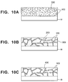
- Fig. 10A through Fig 10C Behavior in the course of change of the coated film in this sol-gel method is shown schematically in Fig. 10A through Fig 10C.
- particles or colloids 100 of the TEOS when coated on a wafer, are in a dispersed state in a solvent 200 (Fig.10A).
- this coated film by being subjected to an basic atmosphere or to heating, is promoted in polycondensation and hydrolysis of the TEOS.
- the coated film is gelled to form a reticular structure of the TEOS 300(Fig.10B).
- the solvent in the coated film is replaced by another solvent 400 of which boiling point is low and surface tension is small (Fig.10C).
- a coated film of a silicon oxide film is obtained.
- a step of replacing the solvent shown in Fig.10C is carried out to remove moisture. Further, the step of replacing with the solvent is carried out with an object to make the film hydrophobic. That is, since OH group is liable to absorb the moisture, the OH group combined to a terminal portion of Si-O bond is replaced by another organic substance by cleaning the film with, for instance, HMDS or the like.
- Another object is to suppress collapse of a structure of the film by employing a solvent of smaller surface tension than ethanol so that a large force is not placed on the reticular structure of the TEOS when the solvent vaporizes.
- a coating unit of coating a coating liquid on a wafer, an aging unit of gelling the coated film by heating the wafer at a pre-determined temperature, for instance, at 100°C, and a replacement unit of replacing the solvent in the coated film by another solvent are necessary.
- a pre-treatment unit for carrying out the pre-treatment such as hydrophobic treatment to the wafer, and a baking unit of drying the wafer are also necessary.
- an apparatus is constituted.
- the gelling treatment needs only to be carried out in a sealed container of an atmosphere filled with vapor of the solvent. That is, after disposing a wafer on a stage heated at a pre-determined temperature in the sealed container, gas including vapor of the solvent needs only to be introduced.
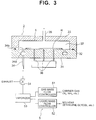
- the aging unit 3 comprises a heating plate 30, a cover 33 provided with a heater, a gas introducing path 34, and a gas exhausting path 35.
- the heating plate 30 is formed of ceramic and incorporates a heater 31a.
- the cover 33 is provided with a heater. This cover 33 is intimately connected to a circumference portion of the heating plate 30 through a sealing member 32, and, together with the heating plate 30, constitutes a sealed container defining a treatment chamber S.
- a gas introducing inlet 34a is formed in slit. This gas introducing inlet 34a penetrates the heating plate 30 and is connected to a gas introducing path 34 introducing gas from the outsides.
- an exhausting outlet 35a is disposed at the central portion of the cover 33.
- This exhausting outlet 35a penetrates the cover 33 to connect the exhausting path 35 communicating with the outsides.
- 3 pieces of pins 36 for going up and down are disposed, for instance, and with these pins for going up and down, the wafer W is moved up and down between the heating plate 30 and the above position thereof.
- a gas of a solvent component for instance, vapor of ethylene glycol
- a gas of a solvent component for instance, vapor of ethylene glycol
- the gas introducing path 34 is disposed penetrating the heating plate 30. Therefore, the gas is introduced into the sealed container after being heated to approximately 100°C, for instance, or a temperature extremely close to that temperature.
- the concentration of the vapor of ethylene glycol is a concentration that is equal with the saturated vapor pressure at a treatment temperature of approximately 100°C, for instance.
- a gas accelerating gelation, ammonia gas for instance, can be introduced simultaneously.
- the first invention of the present application is made to solve such a problem.
- an object of the first invention is to provide a method of coating a film which are capable of suppressing fluctuation of temperature and concentration at the starting time of gas introduction into a sealed container, capable of preventing the solvent component from condensation immediate after transfer of a substrate, for instance, an wafer into the sealed container, and capable of obtaining thereby a thin film, for instance, an interlayer insulating film, of an excellent quality, an aging unit, and an apparatus of coating a film.
- a method of coating a film of the first invention comprises the following steps as disclosed in Claim 1:
- an aging unit for carrying out this method of forming the film comprises:
- an apparatus of forming a film for carrying out the aforementioned method of forming the film comprises:
- the gas introduced into the sealed container in the first gelling step is preferable to be adjusted in temperature to approximately a temperature of the inside of the sealed container.
- the average concentration of the solvent component is made low.
- the concentration of the solvent component is made high. Therefore, immediate after the substrate is transferred into the sealed container, the gas of the solvent component can be prevented from condensation.
- a step of gelling particles or colloids of the coated film is one that heats the substrate.
- the gas to be introduced into the sealed container is made by mixing a carrier gas and the vapor of the solvent component.
- the first gelling step is carried out by adjusting the flow rate of at least one of the carrier gas or the vapor of the solvent component. Further, mixing of the carrier gas and the vapor of the solvent component is carried out at an evaporator which evaporates liquid of the solvent component.
- the first gelling step is carried out by adjusting the flow rate of the liquid of the solvent component being introduced into the evaporator.
- the first gelling step includes the step of varying continuously the concentration of the vapor of the solvent component. Further, the first gelling step includes the step of mixing intermittently the vapor of the solvent component with the carrier gas.
- the second gelling step includes the step of, after the first gelling step is carried out subsequent transfer of the substrate into the sealed container, feeding the gas into the sealed container in a state where the average concentration of the vapor of the solvent component is higher than that during the first gelling step.
- an average concentration of the solvent of the gas being exposed to the substrate at each step is preferable to be the concentration corresponding to the saturated vapor pressure at the substrate temperature at each step.
- the aforementioned first average concentration is preferable to be the concentration corresponding to the saturated vapor pressure at the substrate temperature at the time of introduction of the container, the second average concentration being preferable to be the concentration corresponding to the saturated vapor pressure at the substrate temperature during gelling.
- the inventors investigated to form an interlayer insulating film by use of sol-gel method illustrated in Fig. 10A to Fig.10C.
- HMDS hexamethyl disilane
- the reason for employing heptane here is to suppress collapse of the film structure by avoiding, with use of a solvent of low surface tension, a large power placed on a reticular structure of TEOS during vaporization of the solvent.
- a coating unit for coating a coating liquid on a wafer, a gelling unit for gelling the coated film and a replacement unit for replacing the solvent in the coated film by another solvent are necessary.
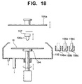
- the resist coating device will be described with reference to Fig.18.
- the device comprises a vacuum chuck 194 which is capable of going up and down and rotates a wafer while holding in a horizontal position, a fixed cup 195, and a nozzle 196 for dispensing a solvent to the wafer.
- the fixed cup 195 is disposed such that it surrounds the wafer W on the chuck 194, and an opening portion at an upper surface is opened or closed by the cup 195a.
- nozzle 196 As the nozzle 196, 3 pieces of nozzles 196a to 196c which discharge ethanol, HMDS and heptane, respectively, are disposed. These nozzles of 196a to 196c are taken out in this order by grasping by a carrying arm 197 from nozzle receiving portions 198a to 198c, and are transferred up to around the central portion above the wafer W.
- the second invention of the present application was made to solve such a problem.
- an object of the second invention of the present application is to provide, in a method of forming a film having a step of carrying out replacement of solvents by dispensing successively at least a plurality of solvents on a surface of a substrate thereon a coated film is to be formed, a method of forming a film, a solvent replacement unit, and an apparatus for forming a film in which a preceding solvent and a succeeding solvent can be supplied continuously, thereby enabling to obtain an excellent thin film such as an interlayer insulating film.
- a method of forming a film of the second invention comprises the following steps disclosed in Claim 13:
- a solvent replacement unit for carrying out this method of coating a film comprises:
- an apparatus of forming a film for carrying out the aforementioned method of forming a film comprises:
- the preceding solvent and the succeeding solvent are continuously supplied on the surface of the coated film without being interrupted.
- the solvent replacement step there is no time of interruption of supply of the solvent on the surface of the substrate thereon the coated film is formed. Therefore, occurrence of such an inconvenience as that occurs due to stoppage of the supply of the solvent, inclusion of moisture in the coated film, for instance, can be suppressed, resulting in formation of an excellent thin film on the substrate.
- the solvent replacement step among the plurality kinds of solvents, at least 2 kinds of solvents may be supplied on a substrate from a common solvent dispensing portion, each of the plurality of kinds of solvents may be supplied on the substrate from separate solvent dispensing portions. Further, in the solvent replacement step, alcohol, a liquid for hydrophobic treatment, and a solvent of smaller surface tension than the solvent contained in the coating liquid, for instance, are supplied in this order on the substrate.
- the inventors attempted to use spin coating, which is used in coating of resist, as a coating method.
- spin coating which is used in coating of resist
- the coating liquid is dripped, the spin chuck is rotated to thin out the coated film over the whole surface through centrifugal force to coat.
- the third invention of the present application was made to solve such a problem.
- an object of the third invention is to provide a method of forming a film, a coating unit, and an apparatus of forming a film which, when obtaining a film by coating a coating liquid dispersed therein starting material of film components of colloids or particles in a solvent on the substrate, enable to obtain a thin film of excellent quality such as an interlayer insulating film.
- the third method of forming a film comprises the following steps as disclosed in Claim 19:
- a coating unit for carrying out this coating method comprises:
- an apparatus of forming a film for carrying out the aforementioned film forming method comprises:
- the third invention after a film is formed on a surface of a substrate, while keeping an atmosphere therein the substrate is placed an atmosphere filled with vapor of the solvent, on the circumference portion of the substrate, a cleaning liquid of removing the coated film may be supplied to remove the coated film of the circumference portion.
- the solvent contains a plurality kinds of organic solvents.
- the third invention includes the case where the vapor is at least one vapor of the plurality kinds of organic solvents.
- the solvent contains ethylene glycol and alcohol
- the vapor of the solvent is ethylene glycol
- the starting material of the film component is a metal alkoxide, for instance.
- the inventors attempted to apply the aforementioned sol-gel method in an actual manufacturing line. That is, the inventors attempted to form a film by, in the step of forming a film, dispensing a coating liquid, in which particles or colloids of TEOS are dispersed in the solvent, on an approximately center of rotation of the wafer surface, then by rotating the wafer around a vertical axis, thereby spreading a coating liquid over the whole surface of the wafer by making use of centrifugal force of rotation.
- a solvent which has a high boiling point and is difficult to evaporate, such as ethylene glycol, is employed.
- the fourth invention of the present application was carried out to solve such a problem.
- an object of the fourth invention is to provide a method of forming a film, a coating unit, and an apparatus of forming a film in which the coating liquid is easily coated on the surface of the substrate, thereby a film is formed universally all over the surface of the substrate, as a result, an excellent thin film such as an interlayer insulating film can be obtained.
- a method of forming a film of the fourth invention comprises the following steps as disclosed in Claim 26:
- tetraethoxysilane can be employed as a starting material. Further, after the step of gelling, on the surface of the substrate thereon a film is formed, the other solvent than the aforementioned one is supplied, thereby the solvent replacement step for replacing the solvent in the coated film by the different solvent may be carried out.
- a coating unit for carrying out this film forming method comprises:
- an apparatus of forming a film for carrying out the aforementioned method for forming a film comprises:
- a solvent of smaller viscosity than that of the component of the most highest viscosity among the components of solvent of the coating liquid is coated over the whole surface of the substrate. Accordingly, when the coating liquid is supplied on the surface thereof, first, the starting material of the coating liquid and water are dissolved in the solution coated over the whole surface of the substrate.
- the viscosity of the coating liquid becomes low. Accordingly, the coating liquid becomes easy to spread on the substrate, to be coated over the whole surface of the substrate universally. As the result, a thin film of excellent quality can be formed.
- one component of lower viscosity than the highest one among the aforementioned components of the solvent may be employed.
- this component and the coating liquid are likely to be easily mixed. And, upon mixing thereof, there is no occurrence of bubbles, accordingly a coated film of more excellent quality can be formed.
- alcohol can be employed as a solution to be coated on the surface of the substrate preceding the step of applying the coating liquid on the surface of the substrate. Since alcohol can dissolve the aforementioned starting materials and water, effect as identical as the aforementioned method of the first disclosure of the fourth invention can be obtained.
- the inventors have studied a method of forming an interlayer insulating film by use of the aforementioned sol-gel method.
- the coating liquid is supplied approximately the center of rotation on the surface of the wafer, then the wafer is rotated.
- the coating liquid is made by mixing TEOS and the solvent in advance, the mixed liquid (coating liquid) is stored in a tank or the like, and the stored coating liquid is supplied on the surface of the wafer.
- the fifth invention of the present application was made to solve such a problem.
- an object of the fifth invention is to provide a method of forming a film which can suppress deterioration of the film quality of the coated film, as a result, can obtain a thin film such as an interlayer insulating film of excellent quality.
- a method of forming a film of the fifth invention comprises the following steps as disclosed in Claim 32:
- the coating liquid is coated on the surface of the substrate.
- the film quality of the coated film can be suppressed from deterioration, resulting in an excellent thin film such as a silicon oxide film.
- a step of cleaning the mixing portion of the first and second liquids and the insides of the liquid path at the downstream of the mixing portion with an organic solvent such as alcohol may be carried out.
- the mixed liquid which remained in the liquid path and lapsed the film quality deteriorating time after mixing is cleared away by the organic solvent. Therefore, upon treatment of the next substrate, the old mixed liquid remaining in the liquid path is not coated, accordingly deterioration of the film quality can be suppressed.
- alcohol when employed as the organic solvent, since alcohol dissolves the starting materials of the film components and water, cleaning of the insides of the liquid path can be carried out readily.
- the inventors have studied another method of forming a film with use of the aforementioned sol-gel method.
- the coated film is gelled.
- heating of the wafer may be one candidate, however, in this case, the solvent in the coated film is activated in evaporation.
- the inventors have studied, as the sixth invention, of carrying out gelation at, for instance, room temperature with use of ammonium gas (NH 3 ) containing water vapor.
- NH 3 ammonium gas
- the reason of containing moisture in ammonium gas is as follows. That is, a part of ammonium gas containing water vapor, upon sticking on the coated film, is ionized such as NH 3 + H 2 O ⁇ NH 4 + + OH - . That is, under presence of water, hydroxide group is formed to be basic. An alkali is a catalyst accelerating polycondensation and contributes to gelation. From this, water vapor is necessary to be contained. And, as the state approaches the saturated state due to much water vapor, OH groups can be expected to be generated much, accordingly the rate of gelation is considered to be fast.
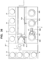
- Fig. 35 a device being used when gelation is carried out with ammonium gas containing water vapor close to the saturated state is illustrated.
- the device 501 comprises a disposing stage 511 of an wafer W, a treatment vessel 510 capable of tight sealing consisting of a sealing member 512 and a cover 513, a tank 521 storing commercial ammonia water (NH 4 OH) (concentration of ammonia : 30% by weight at normal temperature) 520, a bubbling gas supply pipe 522 of carrying out bubbling by introducing ammonia gas into ammonia water 520 in the tank 521, an exhausting outlet 523 of exhausting the treatment gas generated by bubbling, and a piping 525 communicating the exhausting outlet 523 and the gas introducing inlet 514 disposed at the disposing stage 511.
- NH 4 OH commercial ammonia water
- a bubbling gas supply pipe 522 of carrying out bubbling by introducing ammonia gas into ammonia water 520 in the tank 521
- an exhausting outlet 523 of exhausting the treatment gas generated by bubbling and a piping 525 communicating the exhausting outlet 523 and the gas introducing inlet 514 disposed
- ammonia water contains approximately 33% by weight of ammonia as saturated concentration. Therefore, if the bubbling is started at normal temperature with the commercial ammonia water as it is, first, ammonia gas is absorbed in the ammonia water. During this, ammonia gas is not generated or is not generated enough to obtain desired flow rate if generated, accordingly gelation takes a long time. And, when the concentration of ammonia in the ammonia water attains approximately 33% by weight, the ammonia gas containing water vapor of approximately saturated concentration is generated as a treatment gas. The generated treatment gas is introduced into the treatment vessel 510 through the piping 525 and is exhausted out through an exhausting path 515 opened at a cover 513 of the treatment vessel 510.
- the commercial ammonia water is employed as it is. Therefore, when continuous treatment of the wafer is implemented, if ammonia water 520 in the tank 521 is replenished, the concentration of the ammonia water 520 is temporarily lowered and ammonia gas is absorbed. Accordingly, ammonia gas is not generated or, if generated, the desired flow rate can not be obtained. Therefore, there is a problem that gelation can not be completed, accordingly, the desired film thickness and film quality can not be obtained.
- the sixth invention of the present application is made to solve such a problem.
- an object of the sixth invention is, upon gelling the coated film with an ammonia gas, to provide a gas treatment method capable of carrying out stable treatment, and capable of treating evenly between subjects to be treated.
- Another object of the sixth invention is to provide a method capable of carrying out stable treatment, without restricting in the case of carrying out gelling treatment with an ammonia gas, also in the case of carrying out treatment to the subjects to be treated with the treatment gas.
- the method of forming a film of the sixth invention comprises the following steps as disclosed in Claim 36:
- an aging unit for carrying out the method of forming a film comprises:
- an apparatus of forming a film for carrying out the aforementioned method of forming a film comprises:
- ammonia water since the concentration of ammonia in ammonia water is lower than the saturated concentration, when ammonia water is replenished, ammonia gas, upon bubbling by it, is absorbed by ammonia water for a while. Therefore, it takes some time for ammonia gas containing vapor of moisture to be generated with stability.
- the sixth invention when ammonia water is replenished in the precedent container, the first container, for instance, ammonia gas is being generated from the succeeding container, the second container, for instance, accordingly supply of the ammonia gas containing vapor of moisture is not interrupted, thereby stable treatment can be carried out.
- a method of forming a film of the sixth invention comprises the following steps as disclosed in Claim 41:
- a pre-treatment unit for carrying out pre-treatment such as hydrophobic treatment to the wafer, and a bake unit for drying the wafer are also necessary.
- the device is constituted by further disposing a transferring mechanism for transferring the wafer between respective units.
- the solvent being organic solvent, evaporates. If the amount of evaporation is much, there is a problem that the aimed film thickness and film quality can not be obtained.
- the seventh invention of the present application is made to solve such a problem.
- an object of the seventh invention is to provide an apparatus for forming a film capable of carrying out the following step as soon as possible after coating a coating liquid in which particles or colloids of a starting material of a film components are dispersed in a solvent on a substrate and capable of obtaining an excellent thin film such as interlayer insulating film, for instance.
- the apparatus of forming a film of the seventh invention comprises, as disclosed in Claim 44: a coating portion of forming a film by coating a coating liquid, in which particles or colloids of a starting material of a film components is dispersed in a solvent, on a substrate; a gelling treatment portion which is disposed in neighborhood of this coated portion and gels the particles or the colloids in the coated film formed on the coated portion; a plurality of pre-treatment portions for pre-treating prior to coating of the coating liquid on the substrate; a plurality of heating portions for drying the substrate after treatment at the gelling treatment portion; a receiving portion receiving the substrate from the outside; a main transfer portion which, in addition to transferring to the coating portion through the pre-treatment portion after reception of the substrate from the receiving portion, transfers the substrate after treatment at the gelling treatment portion to the heating portion; and an auxiliary transfer portion transferring the substrate coated at the coating portion to the gelling treatment portion.
- the substrate is transferred by an exclusive auxiliary transferring portion from the coating portion to the gelling treatment portion. Therefore, the substrate, immediately after the coating liquid is applied, is transferred to the next step, thereby evaporation of the solvent can be suppressed, resulting in a thin film of excellent film quality.
- a means for feeding vapor of solvent component for instance, ethylene glycol
- a case for covering the coating portion and gelling treatment portion, and a means for feeding vapor of the solvent component into the case may be provided with. In this case, evaporation of the solvent in the coated film during transferring of the substrate can be further suppressed.
- a solvent replacement treatment portion which is disposed neighboring the gelling portion, supplies another solvent different from the aforementioned solvent to the substrate treated at the gelling treatment portion, and replaces the solvent in the coated film by another solvent, can be provided, and the substrate treated at the gelling treatment portion may be transferred to the solvent replacement treatment portion by an auxiliary transferring portion.
- the time period during which large surface tension of the solvent is added on the reticular structure of TEOS is made short, collapse of the film structure is suppressed, resulting in a thin film of excellent quality.
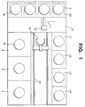
- Fig.1 is a plan view showing diagrammatically an apparatus of forming a film which is employed upon practicing the method of example 1 involving the first invention of the present application.
- Reference numeral 11 denotes an input/output port of wafers W which are substrates.
- a carrying arm 12 At this input/output port 11, from a cassette C disposed on a cassette stage CS, a carrying arm 12, after pulling out an wafer W, supplies to a main arm 13.
- a coating unit 2 which is a coating portion constituting a main portion of the apparatus, together with an aging unit 3 which is a gelling treatment portion and a solvent replacement unit 4 which is a solvent replacing portion, is arranged in this order.
- treatment units U1 to U4 are arranged on the other side of the transferring path 14.
- units for carrying out hydrophobic treatment preceding coating of a coating liquid on the substrate, cooling treatment, and heat treatment (bake treatment) after formation of a film on the substrate or the like are assigned, respectively.
- a coating liquid T id dripped on a surface of the wafer W (Fig.2A).
- a coating liquid one in which colloids and/or particles of TEOS, for instance, is dispersed in a solvent containing ethylene glycol, ethyl alcohol, water and a trace of hydrochloric acid can be employed.
- the inside of the coating unit 2 is filled with vapor of the solvent, ethylene glycol, for instance.
- the coating liquid is spread over a surface of the wafer to form a coated film F (Fig.2B).
- the wafer W is disposed on a heating plate 31 of the aging unit 3, followed by closing of a cover 33 to seal. At this time, the wafer W is heated to a predetermined temperature, approximately 100°C, for instance, by the heating plate 31. Thereafter, vapor of ethylene glycol and a carrier gas are introduced into the aging unit 3 to gel the coated film (Fig.2C).
- HMDS hexamethyl disilane
- heptane solvent replacement of a gelled film is carried out.
- moisture in the coated film is replaced by ethyl alcohol.
- HMDS hydroxide groups in the coated film are removed.
- the solvent in the coated film is replaced by heptane.
- the reason to employ heptane exists in that, due to use of a solvent of lower surface tension, stress added on a porous structure, that is, a reticular structure of TEOS, can be reduced. Thereby, the reticular structure is prevented from collapsing.
- the state up to this step is illustrated in Fig.2D.
- the wafer W is processed for approximately 1min., for instance, at a bake unit.
- an interlayer insulating film consisting of silicon oxide film of a thickness of 6000A, for instance, is formed.
- a gas feeding means 5 is connected to a gas introducing path 34 of the aging unit 3.
- the gas feeding means comprises a gas mass flow controller 51, a liquid mass flow controller 52, a vaporizer 53, a 3-way valve 54 and pipes or tubes connecting them.
- the gas mass flow controller 51 controls flow rate of the carrier gas consisting of a nitrogen gas or an ammonia gas delivered from a carrier gas feeding device (not shown in the figure).
- the liquid mass flow controller 52 controls the flow rate of the solvent such as ethylene glycol delivered from a solvent dispensing device (not shown in the figure).
- a vaporizer 53 vaporizes the solvent controlled in flow rate by the gas mass flow controller 51 and the liquid mass flow controller 52.
- the 3-way valve 54 switches the direction of delivery of the gas containing vapor of the solvent component vaporized by the vaporizer 53 between the chamber side and the exhaust side of the aging unit 3.
- the aging unit 3 has a configuration identical with the unit shown in Fig.11.
- the gas from the gas introducing path 34 is dispersed in a dispersing room 34a and is introduced into a treatment space from a gas introducing inlet 34b formed in slit along the circumference direction.
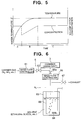
- Fig.4 shows a flow-chart of the gelling treatment.
- a 3-way valve 54 is switched toward the exhaust side.
- a carrier gas and a solvent are supplied from a carrier gas supply device (not shown in the figure) and a solvent supply device (not shown in the figure), respectively.
- a gas mixture of vapor of the solvent component and the carrier gas is formed.
- generated gas mixture is exhausted through the 3-way valve 54 (step 1).
- the coating unit 2 When the state of generation such as concentration, temperature or the like of the gas mixture became stable, in the coating unit 2, the wafer W coated thereon a film is placed on the heating plate 31 kept at the predetermined temperature and the cover 33 is closed (step 2).
- the 3-way valve 54 is switched toward the chamber side.
- the concentration of the solvent component in the gas mixture is adjusted to be the saturated concentration at the treatment temperature, for instance, 100°C (time A in Fig.5).
- the temperature of the wafer W is raised gradually from the normal temperature to fill the insides of the treatment chamber S by the gas mixture, until the temperature of the wafer W reaches the pre-determined temperature T 0 , for instance, 100°C, the average concentration of the solvent component in the gas mixture is made low (time B in Fig.5).
- the concentration of the solvent component is continuously raised as the wafer temperature is elevated.
- the concentration of the solvent component is preferably controlled such that the partial pressure of the solvent component is always equal with the saturated vapor pressure at the wafer temperature, that is, 100% (step S3).
- the concentration control of the solvent component may be carried out by controlling the flow rate of the carrier gas with the gas mass flow controller 51. Or, it can be carried out through control of the liquid mass flow controller 52. Further, both of them may be employed simultaneously.
- the concentration of the solvent component is controlled to be the saturated concentration (100%)(step 4). Then, this state is maintained until gelling treatment of the coated film is completed (time C in Fig.5). Thereafter, by switching the 3-way valve 54 toward the exhaust side, the gas mixture sent from the vaporizer 53 is exhausted (step S5). Then, by opening the cover 33 of the aging unit 3, the wafer W is carried out of the aging unit 3 (step 6). Thereby, the gelling treatment is completed.
- the gas mixture is supplied into a sealed container of the aging unit 3, at the start of gas introduction, fluctuation of the concentration and the temperature of the solvent component can be suppressed. Further, until the temperature of the wafer is elevated to the predetermined temperature after the wafer is carried into the sealed container, the gas concentration of the solvent component in the gas mixture is gradually elevated corresponding to the temperature of the wafer. Therefore, the gas of the solvent component can be prevented from condensing immediately after carrying in of the wafer W into the sealed container, thereby excellent thin film such as an interlayer insulating film can be obtained.
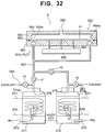
- the gas feeding means 6 comprises a gas mass flow controller 61, a 2-way valve 62, a chamber 63, a heater 64, a feeding pipe 65, a gas mass flow controller 66, a 2-way valve 66a, a 2-way valve 67, and pipes or tubes connecting therebetween.
- the gas mass flow controller 61 controls the flow rate of the carrier gas consisting of a nitrogen gas, an ammonia gas or the like fed from the carrier gas feeder (not shown in the figure).
- the 2-way valve 62 switches feeding or stoppage of the carrier gas regulated in flow rate by the gas mass flow controller 61 to a chamber of the aging unit 3.
- the container 63 stores the solvent such as ethylene glycol or the like.
- the heater 64 heats the solvent.
- the feeding pipe 65 is to pass a bubbling gas such as a nitrogen gas (N 2 gas) fed from the bubbling gas feeder (not shown in the figure) into the solvent such as ethylene glycol solution.
- a bubbling gas such as a nitrogen gas (N 2 gas) fed from the bubbling gas feeder (not shown in the figure) into the solvent such as ethylene glycol solution.
- the gas mass flow controller 66 is to control the flow rate of the solvent vapor generated by a container 63 which is a heating bubbler.
- the 2-way valve 66a is to carry out switching between feed and stoppage of the solvent vapor controlled in flow rate by the mass flow controller 66.
- the 2-way valve 67 switches exhaust and stoppage of the solvent vapor generated by the heating bubbler.
- the carrier gas and the solvent vapor are fed into the chamber 3 after mixing.
- the 2-way valve 67 of the solvent vapor line is closed, for instance, and, by operating either one or both of the mass flow controllers 61, 66, the concentration of the solvent component in the gas mixture can be varied continuously.
- the flow rate of the bubbling gas (N 2 ) is held constant, while exhausting the vapor by opening the 2-way valve 67, only the necessary flow rate may be flowed by controlling the mass flow controller 66. In this case, the pressure in the container 63 is advantageously stabilized.
- the concentration of the solvent component in the gas mixture can be continuously controlled corresponding to the wafer temperature.
- the concentration of ethylene glycol is controlled.
- the solvent vapor of ethylene glycol is kept being generated and exhausted. Therefore, upon starting gas introduction, fluctuation of the temperature and the concentration of the solvent component can be suppressed, in addition, condensation of the gas of the solvent component due to low temperature of the wafer is prevented from occurring, thus, the excellent thin film such as an interlayer insulating film can be obtained.
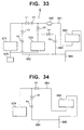
- the gas feeding means 7 shown in Fig.7 is one in which the mass flow controller 61 of the carrier gas line is omitted from the gas feeding means 6 shown in Fig. 6.
- Other constitution is identical as the gas feeding means 6 shown in Fig. 6.
- opening/closing of the 2-way valve 67 of the solvent vapor line may only be switched appropriately.
- the 2-way valve 67 is switched to the chamber 3 side intermittently. Thereby, the time-averaged concentration of the solvent component in the gas atmosphere in the chamber 3 can be adjusted.
- This time in the time interval B as shown in Fig. 8, by making relatively and gradually longer the timings of switching of the 2-way valve 67 toward the chamber 3 side, the average concentration of the solvent component in the gas atmosphere in the chamber 3 can be controlled to be an appropriate concentration corresponding to the elevation of the wafer temperature.
- conductance of the gas flow path is ignored and depiction is made by assuming that the concentration of the gas varies corresponding to the switching of the valve 67.
- the solvent vapor before carrying in of the wafer W, it is preferable the solvent vapor to be kept being generated and exhausted. Also in this example, fluctuation of the concentration and the temperature of the solvent component can be suppressed at the start of gas introduction, further, condensation of the gas of the solvent component due to the wafer of low temperature can be prevented from occurring. Thereby, an excellent thin film such as an interlayer insulating film can be obtained. Further, in the example shown in Fig. 7, by disposing a temperature controlled buffer room 71, the concentration fluctuation of the solvent vapor can be averaged.
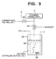
- the gas feeding means 8 shown in Fig. 9, in the gas feeding means 7 shown in Fig. 7, in place of the mass flow controller 66 and the 2-way valve 67, is provided with a 3-way valve 81 which flows the solvent vapor to any one of the chamber 3 side and the exhaust side.
- the solvent vapor By switching appropriately the feeding direction of the solvent vapor between the chamber 3 side and the exhaust side, the solvent vapor can be intermittently fed to the chamber 3 as shown in Fig.8.
- the concentration of the solvent component in the gas atmosphere in the chamber 3 can be controlled such that the appropriate concentration corresponding to the temperature rise of the wafer is attained.
- the piping can be heated with an object to prevent condensation in the piping from occurring.
- the means for generating the solvent vapor is not restricted to a heating bubbler.
- the carrier gas line is dispensed with.
- the solvent concentration and the flow rate of the bubbling gas may be controlled.
- the glass substrate for liquid crystal display can be employed as the substrate to be subjected to treatment.
- fluctuation of the concentration and the temperature of the solvent component can be suppressed at the beginning of gas introduction. Further, condensation of the gas of the solvent component can be prevented from occurring immediately after carrying in the substrate, thereby the excellent thin film such as the interlayer insulating film can be obtained.
- Example 2 involving the second invention will be described. Incidentally, in the following examples, the parts repeating the preceding examples are omitted from explanation.
- the wafer W after being subjected to hydrophobic treatment and cooling treatment, is sequentially carried to the coating unit 2, aging unit 3, and solvent replacement unit 4 by the main arm 13, and, after being carried out respective pre-determined treatments at these units, bake treatment is carried out.
- the coating liquid T is fed (Fig.2A).
- the coating liquid T is spread over the whole surface of the wafer due to the centrifugal force to form a film (Fig.2B).
- the coating liquid T is one in which colloids or particles of TEOS which is a metal alkoxide are dispersed in solvent such as ethylene glycol or ethyl alcohol, for instance, and water and a trace of hydrochloric acid are further contained.
- the colloids of TEOS contained in the coated film on the wafer is gel led to link the colloids in reticulum. Therefore, in the treatment chamber filled by vapor of ethylene glycol, the wafer W is heated to approximately 100°C by the heating plate (Fig.2C). Here, introduction of the vapor of ethylene glycol into the treatment chamber is carried out to suppress vaporization of the solvent in the coated film. Therefore, it is controlled such that, at the temperature in the treatment chamber, for instance, the vapor pressure becomes 100%.
- gelling step instead of heating, by carrying out the treatment at normal temperature in the treatment chamber filled by an ammonia gas, by use of the ammonia gas which is an alkali catalyst, gelling of the colloids of TEOS may be expedited.
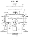
- reference numeral 131 denotes a chuck of holding an wafer W in a level position (an approximate level position can be included).
- This chuck 131 is constituted by a vacuum chuck for instance and sucks and holds the wafer W.
- a rotation axis 133 capable of being gone up and down and rotated by a driving portion 132 is attached.
- the chuck 131 is capable of going up and down between a delivering position of the wafer W which is shown by the dotted line in the figure and is positioned above a cup to be described later and a treatment position of the wafer W shown by the solid line in the figure. Further, the chuck 131 is designed to be rotated around a vertical axis.
- a cup 134 is disposed to in order to surround these.
- an opening 134a where the wafer W is passable is formed on the upper surface of this cup 134.
- the opening 134a can be opened and closed by a cover 135 which is disposed such that it is capable of going up and down.
- a liquid exhaust path 136a and an exhaust gas path 136b are connected.
- 140A is the first nozzle of dispensing alcohol such as ethanol on the surface of the wafer W.
- 140B is the second nozzle of dispensing a hydrophobic treatment liquid such as HMDS.
- the nozzle 140C is the third nozzle of dispensing a solvent such as heptane of smaller surface tension than the solvent contained in the coating liquid.
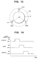
- These nozzles 140A through 140C are disposed with the same distance apart in the circumference direction as shown in Fig. 13. These nozzles 140A through 140C correspond to the respective solvent dispensing portions of the present invention.
- nozzles 140 (140A through 140C) are attached to the inside wall of the cup 134 with the respective attachments 141, and the tip end of each nozzle is attached slantingly to be directed toward the approximately center of rotation O of the surface of the wafer W (the surface thereon a coated film is formed).
- the solvent is dispensed around the center of rotation O of the surface of the wafer W.
- the tip ends of these nozzles are positioned outside the wafer W held by the chuck 131. Therefore, when the chuck 131 which holds the wafer W goes up and down, the wafer W and the each nozzle 140 are designed not to interfere each other.
- the respective nozzles 140 are connected respectively to the ethanol tank 143a, HMDS tank 143b, and heptane tank 143c (not shown in Fig. 12) which are disposed outside the cup 134 by the solvent dispensing path 142 (142a through 142c) inserted from the bottom surface of the cup 134, for instance.
- the solvent dispensing paths 142a through 142c are provided respectively with valves Va through Vc. These valves Va through Vc are controlled in their timings of opening and closing and the degree of opening by a controller 144.
- the step of solvent replacement is carried out as follows. That is, the cover 135 is elevated up to the position shown by the dotted line in Fig.12. At the same time, the chuck 131 is elevated up to the position above the cup 134. Then, at the position shown by the dotted line in Fig.12, by the main arm 13, the wafer W carried up to the unit 4 is delivered to the chuck 131. Then, the chuck 131 is lowered down to the treatment position. At the same time, the cover 135 is lowered down to close the cup 134. Thereafter, the wafer W is rotated.
- the valve Va is opened, thereby ethanol is dispensed around the center of rotation O of the surface of the wafer W from the first nozzle 140A. Due to centrifugal force, the ethanol diffuses over the whole surface of the wafer W. Thereby, ethanol dissolves in the moisture in the coated film. As the result, the moisture is replaced by the ethanol. Incidentally, preceding the rotation of the wafer W, ethanol may be dispensed around the center of rotation O of the surface of the wafer W.
- ethanol is dispensed on the surface of the wafer W, while rotating the wafer W, similarly the valve Vb is opened.
- HMDS is dispensed on the surface of the wafer W from the second nozzle 140B to make diffuse.
- hydroxide groups in the coated film are removed.
- the valve Vc is opened to dispense heptane on the surface of the wafer W from the third nozzle 140C to make diffuse.
- the solvent in the coated film is replaced by heptane.
- the reason why to use heptane is to reduce the force added on the porous structure namely reticular structure of TEOS by use of the solvent of lower surface tension, thereby the reticular structure of TEOS is prevented from collapsing.
- each valve Va, VB and Vc are shown in Fig.14. That is, immediately before closing the valve Va, the valve Vb is opened, further, immediately before closing the valve Vb, the valve Vc is opened. That is, immediately before supply of ethanol completes, supply of HMDS is began. Similarly, immediately before supply of HMDS completes, supply of heptane is started. Thus, it is designed such that a state in which supply of the solvent is stopped does not occur when the solvent to be dispensed to the wafer W is switched.
- the degree of opening of the valve of the solvent of which supply is to be stopped the flow rate of the solvent may be reduced.
- the wafer W undergone the predetermined treatment at the solvent replacement unit 4 is carried up to the bake unit by the main arm 13.
- the wafer W is bake treated at this unit, thereby on the surface of the wafer W, an interlayer insulating film consisting of a silicon oxide film is formed.
- the solvents can be dispensed continuously. Therefore, in the case of the preceding solvents being replaced, compared with the conventional method where opening and closing of the cover and transfer operation of the carrying arm are necessary, the time necessary for the whole solvent replacement treatment can be made remarkably short, and the throughput of the whole treatment can be improved. Further, thus, the time necessary for the solvent replacement step can be made short. As the result, the time period during which the large surface tension of the solvent is added on the reticular structure of TEOS is made short. Therefore, also from this point of view, the film is suppressed from collapsing.
- stoppage of supply of the preceding solvent and start of supply of the succeeding solvent may be carried out simultaneously. Further, by making extremely short the time period between the stoppage of supply of the preceding solvent and the start of supply of the succeeding solvent, supply of the both solvents may be carried out continuously without essentially being interrupted. Even in such a case, supply of the preceding solvent and the succeeding solvent is carried out without essentially being interrupted. As the result, the aforementioned inconvenient phenomena can be suppressed from occurring, thus an excellent thin film can be formed on the substrate.
- the different point of this solvent replacement unit from the aforementioned solvent replacement unit exists in that 3 kinds of solvents are dispensed on the surface of the wafer through a common solvent dispensing portion 150 arranged in a ring.
- the solvent dispensing portion 150 is disposed inside the cup 134 and at the upper side of the outside of the wafer W when the chuck 131 holding the wafer W is positioned at the treatment position, for instance. That is, the solvent dispensing portion 150 arranged in a ring are fixed to a plurality of places of the inside of the cup 134 through the attachment members 151.
- the inside of the solvent dispensing portion 150 is disposed slanted with an expanding diameter toward, for instance, the lower side. On this slanting surface, a plurality of dispensing holes 152 are formed along a circumference direction with an equal distance apart. Thereby, the solvent from the respective dispensing hole 152 is dispensed on around the center of rotation O of the surface of the wafer W. Further, the inside of the solvent dispensing portion 150 is positioned outside the wafer W held by the chuck 131. Therefore, when the chuck 131 holding the wafer W went up and down, the wafer W and the solvent dispensing portion 150 are designed not to interfere each other.
- one end side of the solvent dispensing path 153 inserted from, for instance, the bottom surface of the cup 134 is connected.
- the other end side of the solvent dispensing portion 153 are branched, outside the cup 134, for instance, into 3 dispensing paths 153a through 153c.
- the other end sides of these branched dispensing paths 153a through 153c are connected to a ethanol tank 154a, a HMDS tank 154b, and a heptane tank 154c, respectively.
- valves Va through Vc are inserted, respectively.
- the timing of opening or closing and the degree of opening of these valves Va through Vc are controlled by a controller 144.
- Other configuration is identical as the aforementioned example 2.
- the cup 134 is closed. Thereafter, the valve Va is opened by the controller 144, ethanol is dispensed to the solvent dispensing portion 150 through the solvent dispensing paths 153a and 153. Then, ethanol is dispensed in the neighbor of the center of rotation O on the surface of the wafer W through the dispensing holes 152 from the solvent dispensing portion 150. Then, as identical as the aforementioned embodiments, ethanol is diffused all over the whole surface of the wafer W.
- valve Vb HMDS is dispensed on the surface of the wafer W through the solvent dispensing paths 153b, 153, and the solvent dispensing portion 150.
- valve Vc heptane is dispensed on the surface of the wafer W through the solvent dispensing paths 153c, 153, and the solvent dispensing portion 150.
- the timings of opening and closing of the valves Va, Vb, and Vc are carried out identical as the above example 2.
- Example 4 still another example of the solvent replacement unit for carrying out the step of solvent replacement, that is, Example 4, will be described with reference to Fig. 17.
- the different point of this solvent replacement unit from the aforementioned solvent replacement unit exists in that 3 kinds of solvents are dispensed on the surface of the wafer through a common solvent nozzle 160.
- the solvent nozzle 160 is disposed combined with the cover 135 in such a manner that the tip end of the nozzle 160 pierces through the cover 135 of the cup 134 to oppose the neighborhood of the center of rotation on the surface of the wafer W. Thereby, the solvent is ejected in the neighborhood of the center of rotation of the surface of the wafer W.
- the solvent nozzle 160 corresponds to a common solvent dispensing portion.
- one end side of the solvent dispensing path 161 is connected to this solvent nozzle 160.
- the other end side of the solvent dispensing path 161 is branched into 3 dispensing paths 161a, 161b, and 161c.
- the other end sides of these branched dispensing paths 161a through 161c are connected to a ethanol tank 162a, a HMDS tank 162b, and a heptane tank 162c.
- valves Va through Vc are inserted, respectively. These valves Va through Vc are controlled of their timings of opening and closing and their degree of opening through a controller 144.
- the other configuration is identical as that of the aforementioned example.
- the cup 134 is closed. Thereafter, the valve Va is opened by the controller 144, ethanol is dispensed in the neighborhood of the center of rotation O of the surface of the wafer W through the solvent dispensing portions 161a and 161b, and the solvent nozzle 160. Then, upon the valve Vb being opened, HMDS is dispensed on the surface of the wafer W through the solvent dispensing paths 161b and 161, and the solvent nozzle 160. Subsequently, upon the valve Vc being opened, heptane is dispensed on the surface of the wafer W through the solvent dispensing paths 161c and 161, and the solvent nozzle 160.
- the timings of opening and closing of the valves Va, Vb, and Vc are identical as the example 2.
- the preceding solvent and the succeeding solvent can be dispensed continuously.
- an excellent thin film such as an interlayer insulating film can be obtained.
- Example 5 involving the third invention of the present application will be described.
- Fig.19 an example of a coating unit 2 involving the third invention is illustrated.
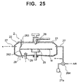
- the coating unit 2 comprises a cup 22 which is a treatment chamber, a vacuum chuck 25 which is disposed inside the cup 22 and functions as a rotary stage holding the wafer, and a coating liquid nozzle 26 for dispensing the coating liquid on the center portion of the wafer W.
- an open inlet for carrying in a substrate 22a is disposed on the upper surface of the cup 22.
- This intake for taking in the substrate 22a is opened and closed by a cover 21 capable of freely going up or down.
- a breakthrough 22b is disposed at the bottom surface of the cup 22 . From this breakthrough 22b, a rotation axis 24 is inserted.
- the upper end of the rotation axis 24 is combined with the vacuum chuck 25, the lower end of the rotation axis is combined with a driving portion 23. Rotating driving force of the driving portion 23 is transmitted to the vacuum chuck 25 through the rotation axis 24. Further, the rotation axis 24 is designed to be capable of going up or down.
- a coating liquid nozzle 26 of dispensing coating liquid on the center portion of the wafer W is attached.
- solvent vapor dispensing pipes 27 for dispensing vapor of the solvent employed in the coating liquid are connected.
- a solvent vapor generator 27a is connected.
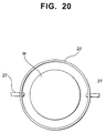
- These solvent vapor dispensing pipes 27 are disposed such that the solvent vapor is dispensed into the cup 22 from a position higher than, for instance, the wafer W disposed on the pre-determined position in the cup 22. Further, as shown in Fig.20, the pipes are disposed in the cup 22 such that the solvent vapor can be dispensed from the both sides of the wafer W.
- the solvent nozzles 262 and 263 for dispensing the solvent which is a cleaning agent for removing (edge-rinse treatment) the coated film at the circumference portion of the wafer, from the solvent dispensing source 261, are inserted.
- the solvent nozzle 263 disposed on the cover 21 is to eject the solvent toward the circumference on the surface side of the wafer W.
- the solvent nozzle 262 disposed on the cup 22 is to remove the coating liquid which goes around the rear surface of the wafer by ejecting the solvent toward the circumference of the rear surface side of the wafer W.
- a drain pipe 28 is connected to the cup 22 .
- an exhaust pipe 29 is connected to the cup 22 .
- a switching valve 29a is connected in the mid-way of the exhaust pipe 29.
- the coating liquid employed here is one in which colloids or particles of TEOS, which is a metal alkoxide, is dispersed in a solvent containing an organic solvent such as ethylene glycol and ethyl alcohol and further water and a trace of hydrochloric acid.
- Ethylene glycol is employed to adjust the viscosity to the most appropriate one for coating the coating liquid.
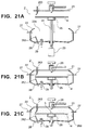
- vapor of ethylene glycol 260 is dispensed inside the cup 22 from the solvent vapor dispensing pipe 27. Then, after the inside of the cup 22 is filled by the vapor 260, the exhaust is stopped.
- the solvent vapor 260 inside the cup 22 at this time is desirable to be the saturated vapor pressure. The reason for this is that, when the vapor pressure is lower than the saturated vapor pressure, the solvent vaporizes from the coating liquid. On the other hand, it is because that, when the vapor pressure is higher than the saturated vapor pressure, that is, when the vapor pressure is in a super-saturated state, the solvent condenses.
- the coating liquid S is dispensed on the center portion of the wafer W from the nozzle 26.
- the coating liquid is spread over the surface of the wafer W due to centrifugal force, to form a coated film.
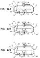
- the rotation speed is lowered and, as shown in Fig.22B, the solvent is sprayed onto the brim of the wafer W from the nozzles 262 and 263.
- the brim portion f of the coated film F spread over the surface of the wafer W is removed.
- the arm is prevented from being contaminated by the coating liquid. Further, when the wafer W is carried to the carrier after completion of the process, particles caused to peel from a part of the coated film due to groove of the carrier are prevented from occurring. Even in this edge rinse-treatment, the inside of the cup 22 is being filled by the solvent vapor 260.
- the treatment after gelling step will be described briefly.
- the gelling step as shown in Fig.24A, after disposing the wafer W on the heating plate 71, the cover 72 is put on to form a sealed space.
- the wafer W is heated to a temperature of, for instance, 100°C to expedite the aforementioned gelling.
- the saturated vapor of ethylene glycol is introduced from the gas introducing path 73 laid inside the heating plate 71, for instance, and is exhausted from the exhaust path 74.
- this gelling step may be carried out by introducing basic gas such as ammonia gas into the treatment chamber.
- the wafer W is placed on the spin chuck 75, on the surface thereof, ethanol and HMDS (hexamethyl disilane) are dispensed in this order. Thereby, moisture and OH groups are removed. Subsequently, by dispensing a liquid of low surface tension such as heptane, the replacement of the solvent is carried out. Thereafter, the wafer W is treated in the bake step to form a porous silicon oxide film.
- HMDS hexamethyl disilane
- the solvent can be suppressed in vaporization from the coated film.
- the edge rinse treatment may be carried out at a different place from the cup 22.
- the inside of the cup 22 is required to be filled with the vapor of the solvent.
- the nozzle can be disposed different from the cup 22, for instance. Then, after the coating liquid is dripped on the wafer W from the nozzle, the cover is closed and the solvent vapor is dispensed into the cup 22. This is also included in the third invention.
- a 3-way valve 264 one end thereof is open to the atmosphere may be disposed.
- the inside of the cup 22 can be exhausted.
- the solvent vapor dispensing pipe 27 can be disposed such that the vapor of the solvent can be dispensed into the cup 22 from 3 or more directions, for instance. Further, by employing an open end cup and by surrounding it by an air tight vessel, the inside thereof is made an atmosphere of the vapor of the solvent and coating may be carried out therein. Further, the edge rinse treatment can be carried out in the open atmosphere, and the coating can be carried out with a method other than the spin coat. Further, as the substrate to be treated, without restricting to the wafer, glass substrates for liquid crystal displays may be employed.
- the coating liquid in which colloids or particles of the starting substances of the film component are dispersed in the solvent can be coated on the substrate while preventing the solvent from evaporating, the excellent thin film such as the interlayer insulating film can be obtained.
- the coated film at the brim portion of the substrate is removed in the atmosphere of the vapor of the solvent, vaporization of the solvent of the coating liquid can be suppressed further more.
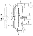
- Fig.26 is a side view of a profile of the coating unit 2 involving example 6.
- reference numeral 331 denotes a chuck holding an wafer W in level (includes a state which is approximately level).
- This chuck 331 is composed of a vacuum chuck, for instance, and is designed to suck and hold the rear surface side of the wafer W.
- a rotation axis 333 capable of going up and down and rotating by a driving portion 332 is attached.
- the chuck 331 is going up and down between a delivering position of the wafer W above the cup which is shown in the figure by the dotted line and will be described later and a treatment position of the wafer W shown in the figure by the solid line.
- the chuck 331 is capable of revolving around a vertical axis.
- a cup 340 is disposed to surround these.
- an opening 341 through which the wafer W is passable is formed on the upper surface of the cup 340.
- This opening 341 is opened or closed by a cover 342 disposed so as to be capable of going up and down.
- a solvent vapor dispensing pipe 351 for dispensing the vapor of the solvent component such as ethylene glycol, which is employed in the coating liquid X and will be described later, into the cup 340 is connected. Further, the vapor of ethylene glycol is generated at the solvent vapor source 352. Further, at the bottom of the cup 340, a drain pipe 353 and an exhaust pipe 354 are connected.
- a coating liquid nozzle 361 for dispensing the coating liquid X approximately on the rotation center of the surface of the wafer (the surface thereon the coated film is formed) and a coating liquid nozzle 362 for dispensing the solution S approximately on the rotation center of the surface of the wafer are disposed.
- These nozzles 361 and 362 are attached slanted combined with the cover 342 such that the respective tip end directs toward the approximate center of rotation on the surface of the wafer.
- the coating liquid X will be described.
- colloids or particles of a metal alkoxide such as TEOS which is a starting component are dispersed in a solvent, and, for the solvent, ethylene glycol, ethyl alcohol, water and a trace of hydrochloric acid are employed.
- An example of the ratio of the respective components in the coating liquid is as follows. For instance, TEOS and water are employed in an equal molar ratio, and ethylene glycol solution and ethanol solution are employed in several times of water by the molar ratio.
- the solution S dispensed on the surface of the wafer from the solution nozzle 62 is preferable to be a solution of smaller viscosity than that of the component of the highest viscosity in the components of the solvent of the coating liquid X, and to be capable of dissolving the metal alkoxide and water.
- the component of the highest viscosity of the components of the solvent of the coating liquid X is ethylene glycol.
- the metal alkoxide such as TEOS or the like is generally insoluble in water, whereas is soluble in alcohol and organic solvent. Therefore, as the solution S capable of being employed in the present example 6, alcohol or organic solvent of smaller viscosity than ethylene glycol can be employed.
- ethanol one of components of the solvent of the coating liquid X, is particularly desirable to be employed.
- the wafer W after being subjected to hydrophobic treatment and cooling treatment, is sequentially carried to a coating unit 2, an aging unit 3, and a solvent replacement unit 4 by a main arm 13, and, after the respective predetermined treatments are carried out at these units, is subjected to bake treatment.
- the cover 342 is elevated up to the position of the dotted line in Fig.26.
- the chuck 331 is elevated up to a position above the cup 340.
- the wafer W carried to the unit 2 by the main arm 13 is delivered to the chuck 331.
- the chuck 331 is lowered to the treatment position, and the cover 342 is lowered to seal the cup 340.
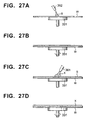
- ethylene glycol vapor is dispensed into the cup 340 from the solvent dispensing pipe 351. Then, after the inside of the cup 340 is filled by the vapor, exhaust is stopped. Then, as shown in Fig.27A, the solution S such as 99.9% ethanol solution for instance is dispensed at the approximate center of rotation of the wafer W from the solution nozzle 362. Then, as shown in Fig.27B, the wafer W is rotated by the chuck 331. Thereby, the solution S is diffused over the whole surface of the wafer W due to centrifugal force, to spread.
- the solution S such as 99.9% ethanol solution for instance
- the coating liquid X is dispensed on the approximate rotation center of the wafer W from the coating liquid nozzle 361.
- the coating liquid X is preferable to be dispensed when the coated solution S is in a state where it does not vaporize and exists on the surface of the wafer W.
- the wafer W is rotated by the chuck 331, the coating liquid X is diffused and spread over the whole surface of the wafer due to centrifugal force, to form the coated film.
- thinner is sprayed on the brim portion of the wafer W from a thinner nozzle in the cup 340, thereby the coated film of the brim portion is removed.
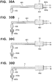
- the inside of the cup 340 is evacuated. Then, by elevating the cover 342 and the chuck 331, the wafer W is delivered to the carrying arm 13 from the chuck 331, and is sequentially transferred to the aging unit 3 and the solvent replacement unit 4. At the respective units 3 and 4, the gelling step and the solvent replacement step are carried out. Then, these steps will be described briefly with reference to Fig.28A and Fig.28B.
- the treatment of gelling the colloids of TEOS contained in the coated film on the wafer W is carried out to link the colloids in a reticular structure.
- a treatment chamber 371 filled by the vapor of ethylene glycol the wafer W is heated to around 100°C by the heating plate (Fig.28A).
- the vapor of ethylene glycol is introduced into the treatment chamber 371 is to suppress vaporization of the solvent in the coated film. Therefore, at the temperature of, for instance, the inside of the treatment chamber 371, vapor is adjusted to be 100%.
- a catalyst such as ammonia can be employed.
- the gelling of the colloids of TEOS may be expedited by the ammonia gas which is a basic catalyst.
- the solvent replacement step by dispensing sequentially ethanol, HMDS (hexamethyl disilane) and heptane on the approximate rotation center of the surface of the wafer W, the solvent in the coated film is replaced by another solvent. Therefore, in the solvent replacement unit 4, as shown in Fig.28B, the wafer W is held in level on the wafer hold 372 constituted to be capable of rotating around the vertical axis.
- 3 pieces of nozzles 373 (373a, 373b, 373c) respectively ejecting ethanol, HMDS, and heptane are prepared. Then, these nozzles 373 (373a, 373b, 373c), by grasping by the carrying arm 374 and pulling out in turn from the respective nozzle receivers which are not shown in the figure, are transferred to the center portion of the wafer W.
- the wafer W is rotated.
- ethanol is dripped on the approximate rotation center of the surface of the wafer W to diffuse over the whole surface of the wafer W due to centrifugal force.
- ethanol dissolves in the moisture in the coated film.
- the moisture is replaced by ethanol.
- HMDS is dripped on the surface of the wafer W.
- OH groups in the coated film are removed.
- heptane is dispensed on the surface of the wafer W.
- the solvent in the coated film is replaced by heptane.
- the reason why to employ heptane is that, due to use of a solvent of low surface tension, the force on a porous structure that is a reticular structure of TEOS can be made small, and the reticular structure of TEOS is made not to collapse.
- the wafer W thereon the predetermined treatment is carried out at the solvent replacement unit 4 is transferred to the bake unit by the main arm 13.
- the wafer W is subjected to the bake treatment.
- an interlayer insulating film consisting of a silicon oxide film is formed on the surface of the wafer W.
- the whole surface of the wafer is coated by ethanol.
- the coating liquid X is dispensed.
- the ethanol since the ethanol is lower in viscosity than ethylene glycol, the ethanol itself readily diffuses over the whole surface of the wafer. Therefore, the ethanol goes into minute concave/convex portions formed on the surface of the wafer W thoroughly.
- the coating liquid X is dispensed, to diffuse.
- the components composing the coating liquid X that is, all of TEOS, water, ethylene glycol and hydrochloric acid are soluble in ethanol. Therefore, the coating liquid X mingles with ethanol on the surface of the wafer W. As the result, the coating liquid X becomes a state of capable of being mingled with ethanol, thereby goes into the places where ethanol exists.
- ethanol is lower in viscosity than ethylene glycol as mentioned above. Therefore, the coating liquid X mingled with ethanol becomes low in viscosity and becomes readily diffused. Therefore, when the wafer W is rotated, the coating liquid X spreads universally on the whole surface of the wafer and goes into the minute concave/convex portions. Therefore, all over the surface of the wafer, the coated film is formed.
- the component of the coating liquid X and the solution S mingle each other.
- the viscosity of the coating liquid X to be spread over the surface of the wafer W becomes low, thereby the similar effect as ethylene glycol can be obtained.
- the solution S and the coating liquid X do not mingle. Therefore, the viscosity of the coating liquid X can not be made low. Furthermore, because of hindrance of the solution S to the coating liquid X, coating on the surface of the wafer W can not be carried out. Incidentally, inclusion of water in the solvent of the coating liquid is not restricted. However, when water is contained, the solution is necessary to be capable of dissolving the starting substance and water.
- a coating liquid X becomes capable of being coated easily on the surface of the wafer W, thereby the coating liquid X can be coated on the whole surface of the wafer W universally. Therefore, since formation of the film can be secured all over the whole surface, as the result, a thin film of excellent quality such as an interlayer insulating film can be formed.
- the aforementioned solvent replacement step is not always necessary.
- a thin film such as an interlayer insulating film may be formed.
- a solution of which viscosity is smaller than that of the component of the highest viscosity among solvents of the coating liquid and is capable of dissolving the starting substance is coated on the surface of the substrate.
- Fig.1 is a plan view showing an apparatus involving example 7.
- Fig.2A through Fig.2D are diagrams showing schematically each step of the method of forming a film involving example 7.
- an wafer W after being subjected to hydrophobic treatment and cooling treatment, is sequentially transferred to a coating unit 2, an aging unit 3, and a solvent replacement unit 4 by a main arm 13, and at these units, the predetermined treatments are carried out, respectively.
- a coating liquid X is dispensed.
- the coating liquid X is spread over the whole surface of the wafer W due to centrifugal force to form a film (treatment of forming a film).
- colloids of TEOS contained in the coated film on the wafer W is gelled, treatment thereby to link the colloids to form a reticular structure is carried out (gelling treatment).
- gelling treatment to carry out this gelling, in a treatment chamber 37 filled by ethylene glycol vapor, the wafer W is heated to approximately 100°C by a heating plate (Fig.2C).
- a heating plate Fig.2C
- treatment instead of heating, in the treatment chamber 37 filled by an ammonia gas, treatment is carried out at the normal temperature, thereby gelling of the colloids of TEOS may be enhanced by the ammonia gas which is a basic catalyst.
- the reason why the inside of the treatment chamber 37 is filled by the ethylene glycol vapor is to suppress vaporization of the solvent in the coating liquid.
- heptane is employed is that, due to use of a solvent of smaller surface tension, the force put on the porous structure, that is, a reticular structure of TEOS, is reduced, thereby the reticular structure of TEOS is prevented from collapsing.
- the wafer W thus carried out the predetermined treatment at the solvent replacement unit 4 is transferred to a bake unit by the main arm 13.
- the wafer W is bake treated at this unit, thereby an interlayer insulating film consisting of a silicon oxide film is formed on the surface of the wafer W.
- the method of forming a film of the fifth invention is characterized in formation treatment of a film.
- Reference numeral 431 in the figure denotes a chuck for holding an wafer W level (includes approximately level).
- This chuck 431 is constituted of a vacuum chuck for instance, the rear side of the wafer W is sucked and held.
- a rotation axis 433 capable of going up and down and rotating by a driving portion 432 is attached.
- the chuck 431 is capable of going up and down between a delivering position of the wafer W above the fixed cup which will be described later and a treatment position of the wafer W shown by the solid line in Fig.29, and is capable of rotating around the vertical axis.
- a fixed cup 440 is disposed in order to surround them.
- an opening 441 where the wafer W is passable is formed on the upper surface of the fixed cup 440.
- the opening portion 441 is opened and closed by a cover 442 disposed to be capable of going up and down.
- a draining pipe 443 and an exhaust pipe 444 are connected on the bottom surface of the fixed cup 440.
- a coating liquid nozzle 450 is attached to dispense the coating liquid which will be described later on the approximate center of the surface of the wafer W (the surface where a coated film is formed).
- This coating liquid nozzle 450 is attached to a supporting arm 451 such that the tip end thereof is directed toward the approximate rotation center of the surface of the wafer.
- the supporting arm 451 is constituted to be capable of moving in a level direction by a driving portion 452.
- the coating liquid nozzle 450 is capable of moving between a dispensing position (a position shown in Fig.29) of dispensing a coating liquid on the surface of the wafer, and a nozzle cleaning portion 453 disposed outside the wafer W which is in the treatment position.
- the nozzle cleaning portion 453 is a portion which receives the liquid overflowing from the coating liquid nozzle 450 and is constituted such that, a liquid exhaust path 453b is connected to the bottom surface of a cylindrical liquid receiver 453a, for instance.
- the coating liquid nozzle 450 is connected to one end side of a solvent dispensing pipe 461 for dispensing a coating liquid X to the nozzle 450.
- the other end side of the coating liquid dispensing pipe 461 is connected to a mixing portion 462.
- This coating liquid dispensing pipe 461 has a jacketed structure having an internal pipe and an external pipe for instance. Through the external pipe, temperature controlling liquid is flowed.
- a plurality, for instance, 2, of reserving tanks 463 and 464 for reserving respectively the first liquid and the second liquid which are components of the coating liquid X are connected through solvent dispensing pipes 463a and 463b having pumps P1 and P2.
- the respective liquids reserved in these first and second reserving tanks 463, 464 are mixed at the mixing portion 462, and are dispensed to the coating liquid nozzle 450 through the coating liquid dispensing pipe 461.
- the coating liquid X will be described.
- colloids or particles of a metal alkoxide such as TEOS which is a starting substance of a film component are dispersed in a solvent.
- a solvent ethanol solution, ethylene glycol, water and a trace of hydrochloric acid (HCl) can be employed.
- the colloids or particles of TEOS are insoluble or difficult to be dissolved in water.
- the liquid in which the colloids or particles of the TEOS, ethylene glycol, water and hydrochloric acid are mixed is reserved in the first reserving tank 463 as the first liquid S1.
- an ethanol solution is an organic solvent which dissolves water and the colloids and the like of TEOS, and is reserved in the second reserving tank 464 as the second liquid S2.
- a cover 442 is elevated up to the position shown by the dotted line in Fig.29.
- a chuck 431 is elevated up to the position above the fixed cup 440.
- the wafer W transferred to the unit 3 by the main arm 13 is delivered onto the chuck 431.
- the chuck 431 is lowered to the treatment position, and the cover 442 is lowered to seal the fixed cup 440.
- the coating liquid X is dispensed on the approximate rotation center on the surface of the wafer W from the coating liquid nozzle 450 to form a coated film on the surface. That is, the coating liquid X (mixed liquid) is made by mixing the first liquid S1 and the second liquid S2 at the mixing portion 462, then this coating liquid X is dispensed on the surface of the wafer W within 6min. after mixing of the respective liquids to coat.
- the predetermined amounts of the first liquid S1 and the second liquid S2 are dispensed to the mixing portion 462 from the first reserving and the second reserving tanks 463 and 464.
- these first and the second liquids S1 and S2 are mixed to prepare the coating liquid X
- the coating liquid X is dispensed on the surface of the wafer W through the coating liquid dispensing pipe 461.
- the coating liquid X is diffused and spread over the whole surface of the wafer due to centrifugal force to form a coated film.
- the predetermined number of the wafers W undergoes film formation.
- a thinner is sprayed on the brim portion of the wafer W from a thinner nozzle in the fixed cup 440 not shown in the figure to remove the coated film of the brim portion.
- the cover 442 and the chuck 431 are elevated to deliver the wafer W from the chuck 431 to the carrying arm 13, then it is carried to the aging unit 3 and the solvent replacement unit 4 in turn.
- the inside of the path of the coating liquid X composed of the mixing portion 462 and the coating liquid pipe 461 is cleaned by an organic solvent. That is, after the coating liquid nozzle 450 is moved above the nozzle cleaning portion 453, supply of the first liquid to the mixing portion 462 is stopped. Then, only the second liquid is dispensed to the coating liquid dispensing pipe 461 through the mixing portion 462.
- the flow path of the coating liquid X is replaced gradually from the upstream side by an organic solvent, the ethanol solution S2 in this example (Fig.30B), before long, is completely replaced by the ethanol solution S2 (Fig.30C).
- the inside of the flow path is cleaned by the ethanol solution S2.
- the coating liquid X and the ethanol solution S2 flowing out of the coating liquid nozzle 450 are exhausted from the liquid exhaust path 453b through the liquid receiver 453a.
- an organic solvent for cleaning the flow path it is preferable to employ a component which dissolves the starting substance of the film component and water.
- organic solvents such as an ethanol solution, IPA (isopropyl alcohol) or the like can be employed.
- the first and the second liquids S1 and S2 are dispensed into the inside of the flow path.
- the coating liquid X by replacing the inside of the flow path by the coating liquid X, then, by moving the coating liquid nozzle 450 to the dispensing position, the wafer W is again subjected to the formation treatment of the coated film. This time, after the coating liquid nozzle 450 is moved to the dispensing position, the inside of the flow path may be replaced by the coating liquid X, or, on the surface of the wafer W, the ethanol solution and the coating liquid X may be replaced.
- the experiments which the inventors carried out are as follows. That is, the aforementioned first liquid S1 and the second liquid S2 are mixed to form the coating liquid X. Then, by varying the time periods up to dispensing the coating liquid X on the surface of the wafers W after mixing, the coated films are formed on the surfaces of the wafers W by the aforementioned method. Then, the state of such formed coated films are observed by visual observation.
- the inventors had grasped from experience that the film quality of the films to be formed deteriorated when the time period up to dispensing on the surface of the wafer W passed approximately 6min. after the first liquid S1 and the second liquid S2 are mixed. Therefore, in order to confirm the critical point, the experiment was carried out by varying the time periods up to dispensing on the surface of the wafers W such as 1min, 2min, 3min, 4min, 5min, 6min, 10min, and 30min, respectively after mixing.
- the in-plane uniformity of the film thickness (standard deviation of film thickness in the wafer plane)/(average film thickness in the wafer plane) ⁇ 100(%) is obtained.
- the obtained coated films are checked by visual observation. The results are shown in Fig.31.
- ⁇ denotes a state where no irregularity is observed in the coated film
- x denotes a state where a radial truck is seen on the surface like a running truck of a particle.
- the coating liquid X which elapsed more than 5min. after mixing of the TEOS and the solvent such as ethanol solution or the like is employed, fluctuation of the film thickness or film quality of the coated film occurs, though the mechanism being not clarified, the inventors assume as follows. That is, the coating liquid X is a mixture of the TEOS and the solvent. When the TEOS and the solvent are mixed, hydrolysis and polymerization of the TEOS occur. When a certain time period elapsed after mixing, the colloids grow too much and deviate from the appropriate colloidal state to obtain the best film quality. As the result, fluctuation in the thickness or the film quality of the coated film are considered to occur.
- TEOS is difficult to dissolve in water but it is soluble in alcohol
- hydrolysis or the polymerization of TEOS is construed to occur after elapse of a certain time period after dissolution of the TEOS, water and hydrochloric acid into the ethanol solution. It is considered that it occurs when the time period of more than 6min. had elapsed after the ethanol solution and the other components were mixed, for instance.
- the coating liquid X by separating the components of the coating liquid X into an ethanol solution (the second liquid) and the other components (the first liquid), and by forming the film while employing the coating liquid X of within 6min. after mixing of these, the coating liquid X can be employed before the colloids grow too much. As the result, it is considered that deterioration of the film quality of the coated film can be suppressed.
- the mixing portion 462 and the flow path of the down stream side of the mixing portion 462 are cleaned. Thereby, in the flow path, there does not remain the old coating liquid which elapsed more than 5min. after mixing. Therefore, when the subsequent wafer W is processed, there is no chance of the old coating liquid X being dispensed on the wafer W, accordingly the film quality of the coated film is prevented from deteriorating.
- the coating liquid may be coated on the surface of the wafer W. Further, vapor of ethylene glycol is dispensed inside the fixed cup 440, after the inside of the cup 440 is filled by the vapor, the coating liquid X may be dispensed. In this case, there is an effect that vaporization of the solvent of the coating liquid X can be suppressed.
- the replacement treatment of the aforementioned solvent is not necessarily required. That is, by carrying out gelling treatment after formation of a coated film, a thin film such as an interlayer insulating film may be formed.
- the first liquid containing particles or colloids of a starting material of a film component and water and the second liquid consisting of an organic solvent capable of dissolving water and the film component are mixed, the mixture of the liquids is coated on the surface of the substrate within 6min. after preparation to form a coated film. Thereby, deterioration of the film quality can be suppressed. As the result, an excellent thin film such as an interlayer insulating film can be obtained.
- the film quality deterioration time period is set at 6min., however, the film quality deterioration time period varies depending on chemicals or solvents to be employed, treatment conditions or the like.
- the appropriate value of the film quality deterioration time period is determined each time by experiment or the like.
- the film quality deterioration time periods are determined. Therefore, in the fifth invention, the film quality deterioration time period is not restricted to 6min.
- Fig.1 is a plan view showing an apparatus involving Example 8.
- Fig.2A through Fig.2D are diagrams showing schematically the respective steps of a method of forming a film involving example 8.
- Fig.2A through Fig.2D the flow of treatment of forming a film is schematically shown in order.
- An wafer W prior to the treatment and taken out by a main arm 13 from the inside of a cassette C of a cassette stage CS is accommodated in a coating unit 2.
- a coating liquid T is dripped on the surface of the wafer W (cf. Fig.2A).
- the coating liquid employed here is one in which colloids or particles of TEOS which is a metal alkoxide are dispersed in a solvent containing organic solvents such as ethylene glycol and ethyl alcohol and further containing water and a trace of hydrochloric acid. Because of low vapor pressure of ethylene glycol, it remains in the film as the solvent even after vaporization of ethyl alcohol, to work for suppressing shrinkage of the film.
- the coating liquid in which sol of TEOS is dispersed in the solvent is spread over the surface of the wafer W to form a film F(Fig.2B).
- the treatment gas is an ammonia gas including water vapor.
- HMDS hexamethyl disilane
- heptane solvent replacement of the gelled film is carried out (Fig.2D).
- moisture in the coated film is replaced by ethyl alcohol.
- OH groups in the coated film are removed by HMDS.
- the solvent in the coated film is replaced by heptane.
- the reason why heptane is employed is to prevent the reticular structure of TEOS from collapsing by decreasing the force put on the porous structure, that is, the reticular structure of TEOS through employment of solvent of small surface tension.
- the wafer W is treated at the bake unit for 1min., for instance.
- an interlayer insulating film consisting of a silicon oxide film is formed.
- Fig.32 is a diagram diagrammatically showing one example of the aforementioned aging unit 3.
- this aging unit 3 comprises a stage 561 thereon the wafer W is placed, a cover 563 sealing the space above the stage 561 together with it, and an exhaust path 565 having an opening in the center portion of the cover 563.
- the cover 563 is intimately connected to the circumference portion of the stage 561 through a sealing member 562, and constitutes the treatment chamber 560 together with the stage 561.
- a plurality of or slit like gas intakes 564 are opened along the outside of the brim of the wafer W placed on the stage 561, a plurality of or slit like gas intakes 564 are opened. Further, on the bottom surface of the aging unit 3, 3 pieces, for instance, of pins 567 capable of going up and down are disposed to be capable of freely appearing and disappearing. These pins 567 capable of going up and down are driven up and down between the stage 561 and the above position thereof by a driving source 566 for going up and down the wafer W.
- the gas intake 564a is connected to a treatment gas dispensing pipe 581.
- This dispensing pipe 581 is branched at the midway, the branched pipes are connected to the first gas generating source 571 and the second gas generating source 572 through switching valves V1 and V2, respectively.
- the first gas generating source 571 and the second gas generating source 572 are constituted in the identical manner.
- first gas generating source 571 and second gas generating source 572 comprise a tank 574a reserving commercial ammonia water (NH 4 OH) (ammonia concentration : 30% by weight at normal temperature) 573, a bubbling gas feeding pipe 575 for carrying out bubbling by introducing an ammonia gas into the ammonia water 573 in the tank 574b, an exhaust takeout 576 exhausting the treatment gas generated by bubbling, and a means 577 for maintaining the temperature of the ammonia water 573 at a constant temperature for instance at the normal temperature.
- the tanks 574a, 574b corresponds respectively to the first chamber and the second chamber in claim 37.
- the tank 574 can be constituted by winding spiral a pipe 578 which is a circulating path of water.
- the pipe 578 is connected to a circulating device of water not shown in the figure and water adjusted to the normal temperature is flowed all the time. Thereby, the temperature of the ammonia water 573 reserved in the tank 574 is always maintained at the normal temperature.
- the treatment gas feeding pipe 581 is branched, between the first gas generating source 571 and the valve V1, and between the second gas generating source 572 and the valve V2, respectively, into bypasses 582, 583 proceeding to the exhaust paths through switching valves V3, V4.
- the ammonia water in the first and the second gas generating sources 571, 572 is maintained at the normal temperature in advance by circulating the temperature controlled water.
- the first gas generating source 571 bubbling of ammonia gas is being carried out and the ammonia gas 573 of the first gas generating source 571 has already reached the saturated concentration of ammonia (approximately 33% by weight).
- the treatment gas consisting of ammonia gas containing water vapor (considered to be in a nearly saturated state) is generated and is exhausted through valve V3.
- the switching valve V2 on the second gas generating source 572 side is closed.
- the wafer W is carried into the treatment chamber 560 from the coating unit 2, thereafter treatment is carried out for the predetermined time period.
- the switching valve V1 on the first gas generating source 571 side is opened, and the valve V3 to the exhaust side is closed, and the treatment gas is dispensed from the first gas generating source 571 to the inside of the treatment chamber 560 (the first treatment step).
- the ammonia water in the first gas generating source 571 decreasing and the ammonia water being replenished thereto
- the ammonia water 573 is made to reach the saturated concentration of ammonia and to generate ammonia gas containing water vapor.
- the switching valve V2 is kept closed, and by opening the valve V4 to the exhaust side, the generated gas is released directly to the exhaust path through the bypass 583 from the second gas generating source 572 (preparatory exhaust step).
- valve V1 which is on the first gas generating source 571 side and was being opened is closed to stop feeding of the treatment gas to the treatment chamber 560 from the first gas generating source 571.
- valve V2 which is on the second gas generating source 572 side and was being closed is opened to feed the treatment gas to the treatment chamber 560 from the second gas generating source 572.
- the valve V3 which is on the first gas generating source 571 side and was being closed is opened. Thereby, the gas generated at the first gas generating source 571 is made to be released to the exhaust path.
- the valve V4 which is on the second gas generating source 572 side and was being opened is closed (the second treatment step).
- the ammonia water is replenished to the first gas generating source 571 to let generate the ammonia gas containing water vapor from the ammonia water which reached the saturated concentration of ammonia by bubbling of ammonia gas.
- the treatment gas feeder is again switched from the second gas generating source 572 to the first gas generating source 571.
- the timing of starting bubbling at the second gas generating source 572 during replenishment of the ammonia water to the first gas generating source 571 is such a timing at which, when the ammonia water is replenished to the first gas generating source 572, a state, where the ammonia gas containing water vapor is generated at the second gas generating source 572, is attained.
- a timing or the timing when the ammonia water at the first and the second gas generating sources 571, 572 is replenished may be determined by an operator. Or, by disposing water level sensors to the respective gas generating sources 571, 572, thereby the water level of the ammonia water may be automatically detected, to determine the appropriate timing.
- switching valves V1, V2, V3, and V4 may be designed to be manually switched by an operator. Or, a controller for controlling switching of these may be disposed to switch automatically according to the predetermined timings.
- Fig.33 is a diagram showing diagrammatically one example of a gas flow path in the aging unit 3 of configuration shown in Fig.32.
- ammonia gas is fed to the first and the second gas generating sources from a common gas feeding source 570.
- a conductance control portion P1 is disposed between the valve V1 and the branching point of the treatment gas feeding pipe 581.
- This conductance control portion P1 is disposed so as to match the conductance from the first gas generating source 571 to the treatment chamber 560 to the conductance from the second gas generating source 572 to the treatment chamber 560.
- This conductance control portion P1 is provided with a structure by which the cross section of the gas flow path, that is, resistance of gas flow can be controlled.
- Specific control of the conductance is carried out such that, by use of a flow meter 580 disposed at the gas feeding pipe 581, the flow rate when the gas is flowed from the first gas generating source 571 and that when the gas is flowed from the second gas generating source are made equal.
- the conductance control portion P1 may be disposed, instead of at the aforementioned position, at positions between from the valve V2 to the aforementioned branching point, or may be disposed on both positions.
- a conductance controlling portion P2 is disposed.
- the conductance of this conductance controlling portion P2 is set the conductance of the whole gas flow path from the first gas generating source 571 through the valve V3 on the exhaust side, the conductance controlling portion P2, and the first bypass 582 to the exhaust path 565, to be equal with the conductance of the whole gas flow path from the first gas generating source 571 through the valve V1 on the treatment chamber side and the treatment chamber 560 to the exhaust path 565.
- the conductance controlling portion P3 is disposed.
- the conductance of this conductance controlling portion P3 is set the conductance of the whole gas flow path from the second gas generating source 572 through the valve V4 on the exhaust side, and the second bypass 583 to the exhaust path 565 to be equal with that of the whole gas flow path from the second gas generating source through the valve V2 on the treatment chamber 560 side and the treatment chamber 560 to the exhaust path 565.
- the gas flow from the first gas generating source 571 to the treatment chamber 560 is stopped, and at the same time, the gas flow from the second gas generating source 572 to the bypass 583 is switched to the valve V2 side.
- the conductances of the respective flow paths were made equal, the pressure and flow rate of the gas flowing into the treatment chamber 560, though being varied a little due to switching of the valve, hardly show fluctuation. This situation is identical when the source of the treatment gas is returned from the second gas generating source 572 to the first gas generating source 571.
- the ammonia water 573 in the first and the second gas generating sources 571, 572 is always being held at the normal temperature by the temperature controlling water, the temperature fluctuation due to vaporization and absorption of ammonia can be suppressed, thereby fluctuation of water vapor is suppressed, resulting in stabilization of the process.
- the generating amount of the gas is considered to fluctuate due to the external temperature disturbance.
- the flow rate of the ammonia gas can be stabilized.
- the ammonia gas is introduced from the beginning with the predetermined pressure and flow rate. Further, even when the first gas generating source and the second gas generating source 571, 572 are switched, the pressure and the flow rate of the ammonia gas do hardly fluctuate, accordingly the gelling treatment can be carried out with stability. As the result, the film thickness and film quality of the coated films can be suppressed from fluctuating, uniform treatment between the wafers can be carried out. Further, since the ammonia water can be replenished without interrupting operation each time, thereby lowering of throughput can be prevented from occurring.
- the temperature control means 577 can maintain the ammonia water 573 in the tank 574 at the normal temperature by winding the tank 574 of the first gas generating source 571 and the second gas generating source 572 by a heater of resistance heating or the like, or by employing an immersion heater.
- the valves V1 and V2 can be substituted by a single 3-way valve.
- the sixth invention can be a configuration in which a single gas generating source 579 generating an ammonia gas saturated by water vapor is connected to the treatment chamber 560.
- the gas generating source 579 can be constituted as identical as the first gas generating source 571 or the second gas generating source 572 shown in Fig.33.
- a switching valve V5 is disposed at the midway of the treatment gas feeding pipe 581 which communicates and connects the gas generating source 579 and the treatment chamber 560.
- a bypass 584 is disposed branched between the valve V5 and the gas generating source 579. This bypass 584 is communicated and connected to the exhaust path 565 through the switching valve V6 and the conductance control portion P4. By conductance control portion P4, the conductance of the flow path through the treatment chamber 560 and that of the flow path through the bypass 584 are made equal.
- the preparatory exhaust step of releasing directly to the exhaust path 565 through the bypass 584 is carried out until the concentration of the ammonia water is stabilized at the predetermined concentration, and when subsequently the flow path is switched to the treatment chamber 560 side, since the conductance of the flow path before and after switching are equal, the ammonia gas can be fed with the predetermined flow rate into the treatment chamber 560 from the beginning, therefore, the stable gelling treatment can be carried out.
- the ammonia gas containing water vapor can be always introduced into the treatment chamber 560. Further, since, through the temperature control of the ammonia water of the gas generating source 579 and the conductance control of the gas flow path, the treatment temperature, the flow rate of the treatment gas and the pressure in the treatment chamber 560 can be held at the constant values, uniform treatment can be carried out between the wafers, thereby the fluctuation of the film quality between the wafers can be suppressed.
- the subject to be treated is not restricted to the wafer, but can be a glass substrate for liquid display device.
- the sixth invention is not restricted to the case of gelling by use of the ammonia gas. It can be applied to a device in which, for instance, while exhausting the treatment gas from the bypass, the subject to be treated is carried into the treatment chamber, thereafter by switching the flow path from the bypass to the treatment chamber side, the treatment gas is introduced.
- the ammonia gas generated therefrom is switched in turn, but 3 and more of tanks 574 can be disposed. In that case, while shifting the timings generating ammonia from the respective tanks 574, by switching 3 tanks 574 and the feeding pipe 581 in turn, the ammonia gas can be flowed always at a constant flow rate.
- the stable treatment in the case of treatment being carried out by introducing the treatment gas into the treatment chamber, the stable treatment can be carried out.
- Fig.36 is a plan view showing diagrammatically the whole configuration of the apparatus of forming a film of example 7 involving the seventh invention of the present application.
- reference numeral 611 denotes an input/output port of wafers W which are substrates
- reference numeral 612 denotes a carrying arm constituting a receiving portion
- reference numeral 613 denotes a main arm constituting a main carrying portion.
- a coating /aging unit 620 provided with a coating unit 620 which is a coating portion and an aging unit 630 which is a gelling treatment portion
- a solvent replacement unit 640 which is a solvent replacement portion
- the treatment units U1 through U4 are arranged.
- the units for carrying out hydrophobic treatment, cooling treatment and heat treatment are respectively assigned.
- the unit for carrying out the hydrophobic treatment and the cooling treatment corresponds to the pre-treatment portion for carrying out the treatment preceding the coating of the coating liquid on the wafer W.
- the unit for carrying out the heat treatment corresponds to the heating portion for drying the wafer W treated at the aging unit 630.
- the carrying arm 612 and the main arm 613 are constituted to be capable of moving freely in the X direction and in the Y direction, and to be capable of rotating freely.
- An wafer W is taken out of a cassette C disposed on a cassette stage CS by the carrying arm 612 and is delivered to the main arm 613. Further, the wafer W is sequentially carried by the main arm 613 to the respective units 620, 640, and U1 through U4.
- the coating/aging unit 620 will be described with reference to Fig.37 through Fig.39.
- a coating unit 620 and an aging unit 630 are disposed adjacent thereto.
- the coating unit 620 comprises a fixed cup 622 for accommodating an wafer W, a cover 621 opening and closing an upper opening thereof, a vacuum chuck 625 disposed to be capable of rotating in the fixed cup 622, and a coating liquid nozzle 626 for dispensing the coating liquid on the wafer W held on the vacuum chuck 625.
- a breakthrough is opened, therethrough a rotation axis 624 is inserted.
- the upper end of this rotation axis 624 is combined with the vacuum chuck 625, the lower end of the other rotation axis 624 is combined to a driving portion 623 disposed below the lower side of the fixed cup 622.
- driving force of rotation is transmitted from the driving portion 623 to the vacuum chuck 625.
- the rotation axis 624 is capable of going up and down in the up/down direction.
- the coating liquid nozzle 626 is disposed combined with the cover 621 and the coating liquid is dispensed on the central portion of the wafer W.
- a solvent vapor feeding pipe 627 for feeding the vapor of the solvent which is sent from the solvent vapor generating source 627a and is employed in the coating liquid is connected.
- a drain pipe 628 and an exhaust pipe 629 are further connected.
- This aging unit 630 comprises a heating plate 631 consisting of ceramic, for instance, including a heater 631a, and a cover 633 disposed adjacent to the upper side of the heating plate 631 so as to form a space S, which constitutes a treatment chamber there, by partitioning the upper space of the heating plate 631.
- the cover 633 is, in addition to being intimately connected to the brim portion of the heating plate 631 through a sealing member 632, free in contacting and detaching with respect to the heating plate 631.
- a groove like gas supply is formed such that surrounds the exterior circumference of the wafer W to be placed on the heating plate 631, the bottom portion of this gas supply is connected to the gas feeding path 634.
- an intake for inhaling a gas is formed, and this intake is connected to an exhaust path 635 communicating with the exterior.
- a heating means such as a heater is preferably disposed even to the cover 633.
- This sub-arm mechanism 5 is exclusively used for carrying the wafer W treated at the coating unit 620 to the aging unit 630.
- this sub-arm 651 is constituted to be capable of moving in the level direction (the X direction in Fig. 1) along a guide rail 652, in addition, the guide rail 652 itself is constituted to be capable of rotating in the level direction through a vertical rotation axis 654 by a driving portion 653.
- the sub-arm 651 is capable of reversing the direction between the coating unit 620 and the aging unit 630 for receiving the wafer W.
- the sub-arm is capable of moving between an waiting position (the position shown by the solid line in Fig.37) and a position receiving the wafer W from the coating unit 620, and between the waiting position and a position delivering the wafer W to the aging unit 630.
- the guide rail 652 is disposed at the above side than the base stage 650.
- a solvent vapor feeding portion 655 which is a means for feeding vapor of the solvent component which is employed in the coating liquid is disposed.
- This solvent vapor feeding portion 655 comprises a dispersing room 656 for dispersing the solvent vapor and a vapor diffusing plate 657.
- the dispersing room 656 is disposed so as to opposes the sub-arm 651 in the waiting position, and the diffusing plate 657 is attached to the bottom surface of the dispersing room 656 and has a structure in which a plurality of steam holes 657a are bored.
- a solvent vapor feeding pipe 658 for instance, for feeding the solvent vapor generated at a solvent vapor generating source, which is not shown in the figure, is connected.
- This unit 640 comprises a vacuum chuck 641 rotating the wafer W while holding it in level, a rotary cup 642 which is disposed to surround the wafer W on this chuck 641 and has a hole 640 for exhausting liquid, a fixed cup 643 which is disposed outside the rotary cup 642 and in which an waste liquid path 641a and an waste gas path 641b are connected, and a nozzle 644 for dispensing the solvent to the wafer W.
- reference numeral 645 in the figure denotes a driving portion for rotating and going up and down the rotation axis 641a of the chuck 641
- reference numeral 642a denotes a driving portion for rotating the rotary cup 640.
- the opening on the upper surface of the fixed cup 643 is opened and closed by a cover 646 capable of going up and down.
- a cover 646 capable of going up and down.
- the wafer W undergone the hydrophobic treatment and the cooling treatment is carried in turn to the coating/aging unit 620, the solvent replacement unit 640, and the unit for carrying out bake treatment, and by carrying out the predetermined treatment at the respective units, an interlayer insulating film consisting of a silicon oxide film is formed on the surface of the wafer W.
- the coating liquid is coated on the surface of the wafer W at the coating unit 620 to form a coated film.
- the wafer W is carried to the aging unit 630 by the sub-arm 651. Then, the particles or the colloids of the coated film formed on the wafer W at the unit 630 are gelled.
- the wafer W carried to the coating unit 620 by the main arm 613 is delivered to the chuck 625 at the position of the dotted line in Fig.38 for instance, after the chuck 625 is lowered, the cup 622 is sealed by the cover 621.
- the coating liquid used here can be prepared by dispersing the colloids or particles of TEOS which is a metal alkoxide in the solvent which contains organic solvent such as ethylene glycol and ethyl alcohol, water and a trace of hydrochloric acid.
- Ethylene glycol plays, other than the role of, upon coating, adjusting the viscosity of the coating liquid to an appropriate value, another role of suppressing vaporization of ethyl alcohol by remaining there as the solvent because, at the steps after the coating step, ethyl alcohol the vapor pressure of which is low vaporizes almost completely. This is based on the higher vapor pressure of ethylene glycol.
- the vapor of ethylene glycol is fed into the cup 622 from the solvent vapor feeding pipe 627.
- the exhausting is ceased after the inside of the cup 622 is filled by the vapor of ethylene glycol, and the coating liquid is fed on the central portion of the wafers W from the nozzle 626.
- the wafer W is rotated by the chuck 625, the coating liquid is spread on the surface of the wafer W due to centrifugal force to form a film.
- the reason why the treatment is carried out in such a state where the inside of the cup 622 is filled by the vapor of ethylene glycol is to suppress the vaporization of the solvent in the coating liquid.
- the solvent is sprayed on the circumference portion of the wafer W from the nozzle in the cup 622 to remove the coated film of the circumference portion.
- the wafer W is carried to the aging unit 630 by the sub-arm 651.
- the wafer W is delivered from the chuck 625 to the sub-arm 651.
- the solvent vapor such as that of ethylene glycol is fed on the guide rail 652 from the solvent vapor feeding portion 655, the direction of the sub-arm 651 is turned to the side of the coating unit 620, the sub-arm 651 is moved from the waiting position to the position where the wafer W is received from the coating unit 620, and the wafer W is delivered from the chuck 625 to the sub-arm 651.
- the cover 633 of the aging unit 630 is raised, the direction of the sub-arm 651 is turned to the side of the aging unit 630, the sub-arm 651 is moved to the position where the wafer W is delivered to the aging unit 630, by cooperation of the pins 636 for going up and down and the sub-arm 651, the wafer W is delivered from the sub-arm 651 on the heating plate 631.
- the colloids of TEOS contained in the coated film on the wafer W is gelled, to link the colloids reticular. That is, at the aging unit 630, after the wafer W is placed on the heating plate 631, the cover 633 is closed, while evacuating from the exhaust path 635, the vapor of ethylene glycol for instance is introduced into the treatment chamber from the gas feeding path 634. Here, the wafer W is heated to the temperature of around 100°C, for instance.
- the treatment of linking the colloids reticular by gelling the colloids of TEOS is expedited by heating the coated film, however, by employing an ammonia gas instead of heating, the ammonia gas is operated on TEOS as a catalyst, thereby the gelling may be expedited.
- the reason why the vapor of ethylene glycol is introduced into the treatment chamber is to suppress the vaporization of the solvent in the coated film, therefore, the piping and the vapor generating source are controlled in their temperature such that the vapor is saturated (100% by the relative humidity of ethylene glycol) at the temperature of the treatment chamber, for instance.
- the wafer W treated at the aging unit 630 is delivered from the heating plate 631 to the main arm 613, then is transferred to the solvent replacement unit 640 by this main arm 613. And, at this unit 640, a solvent other than the solvent of the coating liquid is fed, thereby the solvent in the coated film formed on the wafer W is replaced by the other solvent.
- the wafer W is delivered to the chuck 641 from the main arm 613, and the chuck 641 is lowered. Then, first, together with dripping chemicals in which moisture is soluble, for instance, ethanol on the approximately central portion of the wafer W from the nozzle 644a, the wafer W and the rotary cup 642 are rotated, thereby ethanol is diffused over the whole surface of the wafer W due to the centrifugal force. Thereby, ethanol dissolves in the moisture in the coated film, resulting in replacement of the moisture by ethanol.
- HMDS HMDS
- heptane a structure with only a fixed cup may be employed.
- the coating unit 620 and the aging unit 630 are disposed adjacently inside the same unit 620, thereby the wafer W is transferred by an exclusive sub-arm 651 from the coating unit 620 to the aging unit 630. Therefore, the wafer W on which the coating treatment is carried out at the coating unit 620 is transferred without delay to the aging unit 630 without waiting transfer of the wafer W and is treated. Accordingly, since gelling treatment can be carried out in a state where the vaporization of the solvent in the coated film is suppressed, desired film thickness and film quality can be secured.
- the distance of the transfer path between the coating unit 620 and the aging unit 630 is short, accordingly the transfer time becomes short. Accordingly, vaporization of the solvent in the coated film during transfer can be reduced further more. Further, since the vapor of ethylene glycol is supplied on the transfer path, the vaporization of the solvent during transfer is further suppressed by this ethylene glycol.
- a solvent vapor feeding pipe 664 for feeding the vapor of ethylene glycol generated at the solvent vapor generating source 663 and an exhaust pipe 665 are connected respectively.
- a means for feeding the vapor of the solvent component into the treatment chamber 660 is constituted of the solvent vapor generating source 663 and the solvent vapor feeding pipe 664.
- the inside of the treatment chamber 660 is adjusted to be saturated by the vapor of ethylene glycol. Then, in a state where the inside of the treatment chamber 660 is made the atmosphere of ethylene glycol, the door 662a is opened, the wafer W is delivered from the main arm 613 on the chuck 625 of the coating unit 620, and the door 662a is closed. Then, treatment for forming a coated film is carried out as described above, the wafer W is transferred from the coating unit 620 to the aging unit 630 by the sub-arm 651, and at the aging unit 630 gelling treatment is carried out. Thereafter, the door 662b is opened, and the wafer W is delivered from the heating plate 631 to the main arm 613.
- a coating unit 620 and an aging unit 630 and a solvent replacement unit 640 are disposed adjacently in the same unit 670 in this order, and, between the aging unit 630 and the solvent replacement unit 640, a sub-arm mechanism 672 constituting an auxiliary transfer portion for transferring exclusively the wafer W treated at the aging unit 630 to the solvent replacement unit 640 is disposed.
- a sub-arm mechanism 650 for exclusively transferring the wafer W treated at the coating unit 620 to the aging unit 630 is disposed, the sub-arm mechanism 670 between the aging unit 630 and the solvent replacement unit 640 is constituted identically as the sub-arm mechanism 650. That is, the sub-arm 671, together with the direction being reversed between the aging unit 630 and the solvent replacement unit 640, is constituted to be capable of moving along the guide rail (transferring path) 672 between the both units 630, 640.
- the wafer W is delivered from the main arm 613 onto the chuck 625 of the coating unit 620, after the coating treatment is carried out at the coating unit 620, the wafer W is transferred to the aging unit 630 by the sub-arm 651, to deliver to the heating plate 631. Then, after the gelling treatment is carried out at this unit 630, the wafer W is delivered to the sub-arm 671 to transfer to the solvent replacement unit 640, then is delivered to the chuck 641. And, after solvent replacement treatment is carried out at this unit 640, the wafer W is delivered from the chuck 641 to the main arm 613, and the wafer W is transferred by the arm 613 to a unit for carrying out bake treatment.
- the auxiliary transfer portion may be constituted as shown in Fig.44.
- a coating unit 620, an aging unit 630, and a solvent replacement unit 640 are constituted as different units each other.
- the auxiliary transfer portion 680 is provided with a pair of arm members 681a, 681b which hold the wafer W by nipping a part of both circumference portions of the wafer W for instance, and these arm members 681a, 681b are constituted to be capable of freely opening and closing in the Y direction for instance by an opening and closing mechanism 682.
- the opening and closing mechanism 682 is constituted to be movable in the X direction along the guide rail 683 at a position above the respective units 620, 630, and 640.
- the wafer W is exclusively transferred along the guide rail 683 from the coating unit 620 to the aging unit 630, and from the aging unit 630 to the solvent replacement unit 640, held by the arm members 681a, 681b.
- this auxiliary transfer portion can be applied even in the case of the coating unit 620, the aging unit 630, and the solvent replacement unit 640 being constituted as the same unit, also can be applied for transfer only between the coating unit 620 and the aging unit 630.
- Reference numeral 691 in the figure denotes a main arm constituted to be capable of freely going up and down, freely moving forward and backward, and freely rotating, and, on one side (left side) of the main arm 691, a hydrophobic treatment unit 692 which is a pre-treatment step for carrying out the hydrophobic treatment of the wafer W, and 5 heating units 693a through 693e, for instance, constituting the heating portion for carrying out heat treatment (bake treatment) to the wafer W are piled up from the bottom in this order.
- a receiving portion 694 for receiving the wafer W from outside the apparatus a coating unit 620, an aging unit 630, and a solvent replacement unit 640 are piled up from the bottom in this order.
- a plurality of unit groups are disposed respectively, and, between these unit groups, a transfer path of the main arm 691 is formed.
- the sub-arm 696 constituting the auxiliary transfer portion is disposed to be capable of freely going up and down, freely moving forward and backward, and freely rotating, and the inside of the case 695 is a transfer path of the sub-arm 696.
- the wafer W is exclusively transferred between the coating unit 620 and the aging unit 630 by the sub-arm 696, transfer between these units 620, 630 is carried out without delay. Accordingly, vaporization of the solvent in the coated film can be suppressed and the film quality of the thin film is prevented from deteriorating.
- the inside of the case 695 may be made an atmosphere of ethylene glycol, or, by extending the case 695 up to the side of the solvent replacement unit 640, the wafer W may be exclusively transferred between the aging unit 630 and the solvent replacement unit 640 by the sub-arm 696.
- the substrate is not restricted to the wafer but can be glass substrate for liquid crystal display.
- the subsequent step can be carried out without delay, accordingly a thin film of excellent quality such as an interlayer insulating film can be obtained.
Landscapes
- Formation Of Insulating Films (AREA)
- Application Of Or Painting With Fluid Materials (AREA)
Priority Applications (2)
| Application Number | Priority Date | Filing Date | Title |
|---|---|---|---|
| EP03026463A EP1411543B1 (de) | 1997-12-15 | 1998-12-15 | Vorrichtung zum Härten einer Beschichtung und Vorrichtung zum Beschichten |
| EP05000580A EP1523031B1 (de) | 1997-12-15 | 1998-12-15 | Vorrichtung zum Härten einer Beschichtung und Vorrichtung zum Beschichten |
Applications Claiming Priority (14)
| Application Number | Priority Date | Filing Date | Title |
|---|---|---|---|
| JP36355297A JP3273754B2 (ja) | 1997-12-15 | 1997-12-15 | 塗布膜形成装置 |
| JP36355297 | 1997-12-15 | ||
| JP1321798 | 1998-01-07 | ||
| JP01321798A JP3225220B2 (ja) | 1998-01-07 | 1998-01-07 | 塗布膜形成方法 |
| JP01496598A JP3193898B2 (ja) | 1998-01-09 | 1998-01-09 | 塗布膜形成方法 |
| JP1496598 | 1998-01-09 | ||
| JP01496498A JP3173725B2 (ja) | 1998-01-09 | 1998-01-09 | 塗布膜形成方法、液処理方法及び液処理装置 |
| JP1496498 | 1998-01-09 | ||
| JP03050298A JP3432735B2 (ja) | 1998-01-27 | 1998-01-27 | 塗布膜形成装置 |
| JP3050298 | 1998-01-27 | ||
| JP7333698 | 1998-03-05 | ||
| JP07333698A JP3200586B2 (ja) | 1998-03-05 | 1998-03-05 | 塗布膜形成方法及びその装置 |
| JP09249698A JP3200587B2 (ja) | 1998-03-20 | 1998-03-20 | ガス処理方法 |
| JP9249698 | 1998-03-20 |
Related Child Applications (1)
| Application Number | Title | Priority Date | Filing Date |
|---|---|---|---|
| EP03026463A Division EP1411543B1 (de) | 1997-12-15 | 1998-12-15 | Vorrichtung zum Härten einer Beschichtung und Vorrichtung zum Beschichten |
Publications (2)
| Publication Number | Publication Date |
|---|---|
| EP0928638A2 true EP0928638A2 (de) | 1999-07-14 |
| EP0928638A3 EP0928638A3 (de) | 2000-05-24 |
Family
ID=27563646
Family Applications (2)
| Application Number | Title | Priority Date | Filing Date |
|---|---|---|---|
| EP03026463A Expired - Lifetime EP1411543B1 (de) | 1997-12-15 | 1998-12-15 | Vorrichtung zum Härten einer Beschichtung und Vorrichtung zum Beschichten |
| EP98310263A Withdrawn EP0928638A3 (de) | 1997-12-15 | 1998-12-15 | Verfahren zum Beschichten eines Substrates und Vorrichtung zum Beschichten und Härten der Beschichtung |
Family Applications Before (1)
| Application Number | Title | Priority Date | Filing Date |
|---|---|---|---|
| EP03026463A Expired - Lifetime EP1411543B1 (de) | 1997-12-15 | 1998-12-15 | Vorrichtung zum Härten einer Beschichtung und Vorrichtung zum Beschichten |
Country Status (4)
| Country | Link |
|---|---|
| US (5) | US6248168B1 (de) |
| EP (2) | EP1411543B1 (de) |
| KR (2) | KR100524205B1 (de) |
| DE (1) | DE69833985T2 (de) |
Cited By (2)
| Publication number | Priority date | Publication date | Assignee | Title |
|---|---|---|---|---|
| EP1341224A4 (de) * | 2000-11-17 | 2005-01-26 | Matsushita Electric Industrial Co Ltd | Verfahren zur herstellung eines halbleiterbauelements |
| DE19952604B4 (de) * | 1998-11-04 | 2006-07-06 | Tokyo Electron Ltd. | Vorrichtung zum Ausbilden eines Beschichtungsfilms |
Families Citing this family (466)
| Publication number | Priority date | Publication date | Assignee | Title |
|---|---|---|---|---|
| US6977098B2 (en) * | 1994-10-27 | 2005-12-20 | Asml Holding N.V. | Method of uniformly coating a substrate |
| US7018943B2 (en) | 1994-10-27 | 2006-03-28 | Asml Holding N.V. | Method of uniformly coating a substrate |
| US7030039B2 (en) * | 1994-10-27 | 2006-04-18 | Asml Holding N.V. | Method of uniformly coating a substrate |
| US6248168B1 (en) * | 1997-12-15 | 2001-06-19 | Tokyo Electron Limited | Spin coating apparatus including aging unit and solvent replacement unit |
| US6287987B1 (en) * | 1999-04-30 | 2001-09-11 | Lsi Logic Corporation | Method and apparatus for deposition of porous silica dielectrics |
| US6616760B2 (en) * | 1999-12-17 | 2003-09-09 | Tokyo Electron Limited | Film forming unit |
| JP3648129B2 (ja) * | 2000-05-10 | 2005-05-18 | 東京エレクトロン株式会社 | 塗布現像処理方法及び塗布現像処理システム |
| US6481447B1 (en) * | 2000-09-27 | 2002-11-19 | Lam Research Corporation | Fluid delivery ring and methods for making and implementing the same |
| JP3741604B2 (ja) | 2000-11-27 | 2006-02-01 | 東京エレクトロン株式会社 | 熱処理装置および熱処理方法 |
| KR100857972B1 (ko) * | 2001-06-07 | 2008-09-10 | 도쿄엘렉트론가부시키가이샤 | 도포막 형성방법 및 도포막 형성장치 |
| US6683006B2 (en) * | 2001-06-25 | 2004-01-27 | Tokyo Electron Limited | Film forming method and film forming apparatus |
| US7011864B2 (en) * | 2001-09-04 | 2006-03-14 | Tokyo Electron Limited | Film forming apparatus and film forming method |
| JP3992480B2 (ja) * | 2001-11-12 | 2007-10-17 | 東京エレクトロン株式会社 | 基板処理装置および基板処理方法ならびに基板処理システム |
| US6843852B2 (en) * | 2002-01-16 | 2005-01-18 | Intel Corporation | Apparatus and method for electroless spray deposition |
| JP4352783B2 (ja) * | 2002-08-23 | 2009-10-28 | 東京エレクトロン株式会社 | ガス供給系及び処理システム |
| US6875467B2 (en) * | 2002-12-15 | 2005-04-05 | Optinetrics, Inc. | Crack resistant sol-gel wafer coatings for integrated optics |
| JP2004228335A (ja) * | 2003-01-23 | 2004-08-12 | Sony Corp | 水蒸気酸化装置 |
| US7341630B1 (en) * | 2003-06-26 | 2008-03-11 | Advanced Cardiovascular Systems, Inc. | Stent coating system |
| JP2005082880A (ja) * | 2003-09-11 | 2005-03-31 | Shoka Kagi Kofun Yugenkoshi | 有機el発光装置の成膜設備 |
| JP3740485B2 (ja) * | 2004-02-24 | 2006-02-01 | キヤノン株式会社 | 電子放出素子、電子源、画像表示装置の製造方法及び駆動方法 |
| US7779782B2 (en) * | 2004-08-09 | 2010-08-24 | Lam Research | Systems and methods affecting profiles of solutions dispensed across microelectronic topographies during electroless plating processes |
| US7651306B2 (en) | 2004-12-22 | 2010-01-26 | Applied Materials, Inc. | Cartesian robot cluster tool architecture |
| US7819079B2 (en) | 2004-12-22 | 2010-10-26 | Applied Materials, Inc. | Cartesian cluster tool configuration for lithography type processes |
| US7798764B2 (en) | 2005-12-22 | 2010-09-21 | Applied Materials, Inc. | Substrate processing sequence in a cartesian robot cluster tool |
| US20060130767A1 (en) | 2004-12-22 | 2006-06-22 | Applied Materials, Inc. | Purged vacuum chuck with proximity pins |
| US7699021B2 (en) | 2004-12-22 | 2010-04-20 | Sokudo Co., Ltd. | Cluster tool substrate throughput optimization |
| US7228645B2 (en) * | 2005-01-11 | 2007-06-12 | Xuyen Ngoc Pham | Multi-zone shower head for drying single semiconductor substrate |
| JP4367347B2 (ja) * | 2005-01-21 | 2009-11-18 | セイコーエプソン株式会社 | 膜形成方法及び電気光学装置の製造方法並びに電子機器 |
| KR100696378B1 (ko) * | 2005-04-13 | 2007-03-19 | 삼성전자주식회사 | 반도체 기판을 세정하는 장치 및 방법 |
| KR100706793B1 (ko) * | 2005-08-03 | 2007-04-12 | 삼성전자주식회사 | 케미컬 공급 장치 및 케미컬 공급 방법 |
| US7807336B2 (en) | 2005-12-28 | 2010-10-05 | Hynix Semiconductor Inc. | Method for manufacturing semiconductor device |
| JP5137366B2 (ja) * | 2006-01-24 | 2013-02-06 | 株式会社日立国際電気 | 基板処理システム及び液体材料供給装置 |
| JP4999415B2 (ja) * | 2006-09-29 | 2012-08-15 | 東京エレクトロン株式会社 | 基板処理装置及び基板処理方法並びに基板処理装置の用力供給装置及び基板処理装置の用力供給方法 |
| JP4842771B2 (ja) * | 2006-11-15 | 2011-12-21 | 東京エレクトロン株式会社 | 処理システムと処理方法および記録媒体 |
| JP4803821B2 (ja) * | 2007-03-23 | 2011-10-26 | 大日本スクリーン製造株式会社 | 基板処理装置 |
| GB2447919B (en) * | 2007-03-27 | 2012-04-04 | Linx Printing Tech | Ink jet printing |
| JP4466966B2 (ja) * | 2007-11-22 | 2010-05-26 | 東京エレクトロン株式会社 | 基板処理装置 |
| KR101538187B1 (ko) * | 2007-11-30 | 2015-07-22 | 갈데르마 리써어치 앤드 디벨로프먼트 | 하나 이상의 나프토산 유도체, 과산화 벤조일 및 하나 이상의 필름-형성제를 함유하는 조성물 |
| EP2241442B1 (de) * | 2008-01-28 | 2011-10-26 | Hitachi Industrial Equipment Systems Co., Ltd. | Tintenstrahlaufzeichnungsvorrichtung |
| US10378106B2 (en) | 2008-11-14 | 2019-08-13 | Asm Ip Holding B.V. | Method of forming insulation film by modified PEALD |
| JP5359285B2 (ja) * | 2009-01-07 | 2013-12-04 | 東京エレクトロン株式会社 | 処理装置及び処理装置の運転方法 |
| US9394608B2 (en) | 2009-04-06 | 2016-07-19 | Asm America, Inc. | Semiconductor processing reactor and components thereof |
| US8802201B2 (en) | 2009-08-14 | 2014-08-12 | Asm America, Inc. | Systems and methods for thin-film deposition of metal oxides using excited nitrogen-oxygen species |
| JP5795917B2 (ja) * | 2010-09-27 | 2015-10-14 | 株式会社Screenホールディングス | 基板処理装置および基板処理方法 |
| KR101147305B1 (ko) * | 2010-10-12 | 2012-05-18 | 나노씨엠에스(주) | 나노 금속성 은의 침착에 의한 나노 은 박막 형성장치 |
| JP2012084789A (ja) * | 2010-10-14 | 2012-04-26 | Toshiba Corp | 半導体装置の製造方法および半導体製造装置 |
| US9312155B2 (en) | 2011-06-06 | 2016-04-12 | Asm Japan K.K. | High-throughput semiconductor-processing apparatus equipped with multiple dual-chamber modules |
| US9793148B2 (en) | 2011-06-22 | 2017-10-17 | Asm Japan K.K. | Method for positioning wafers in multiple wafer transport |
| US10364496B2 (en) | 2011-06-27 | 2019-07-30 | Asm Ip Holding B.V. | Dual section module having shared and unshared mass flow controllers |
| US10854498B2 (en) | 2011-07-15 | 2020-12-01 | Asm Ip Holding B.V. | Wafer-supporting device and method for producing same |
| US20130023129A1 (en) | 2011-07-20 | 2013-01-24 | Asm America, Inc. | Pressure transmitter for a semiconductor processing environment |
| US9341296B2 (en) | 2011-10-27 | 2016-05-17 | Asm America, Inc. | Heater jacket for a fluid line |
| US9096931B2 (en) | 2011-10-27 | 2015-08-04 | Asm America, Inc | Deposition valve assembly and method of heating the same |
| US9017481B1 (en) | 2011-10-28 | 2015-04-28 | Asm America, Inc. | Process feed management for semiconductor substrate processing |
| US9167625B2 (en) | 2011-11-23 | 2015-10-20 | Asm Ip Holding B.V. | Radiation shielding for a substrate holder |
| US9005539B2 (en) | 2011-11-23 | 2015-04-14 | Asm Ip Holding B.V. | Chamber sealing member |
| US9202727B2 (en) | 2012-03-02 | 2015-12-01 | ASM IP Holding | Susceptor heater shim |
| US8946830B2 (en) | 2012-04-04 | 2015-02-03 | Asm Ip Holdings B.V. | Metal oxide protective layer for a semiconductor device |
| US8728832B2 (en) | 2012-05-07 | 2014-05-20 | Asm Ip Holdings B.V. | Semiconductor device dielectric interface layer |
| US8933375B2 (en) | 2012-06-27 | 2015-01-13 | Asm Ip Holding B.V. | Susceptor heater and method of heating a substrate |
| US9499390B1 (en) * | 2012-07-17 | 2016-11-22 | Global Agricultural Technology And Engineering, Llc | Liquid delivery system |
| US9558931B2 (en) | 2012-07-27 | 2017-01-31 | Asm Ip Holding B.V. | System and method for gas-phase sulfur passivation of a semiconductor surface |
| US9117866B2 (en) | 2012-07-31 | 2015-08-25 | Asm Ip Holding B.V. | Apparatus and method for calculating a wafer position in a processing chamber under process conditions |
| US9659799B2 (en) | 2012-08-28 | 2017-05-23 | Asm Ip Holding B.V. | Systems and methods for dynamic semiconductor process scheduling |
| US9169975B2 (en) | 2012-08-28 | 2015-10-27 | Asm Ip Holding B.V. | Systems and methods for mass flow controller verification |
| US9021985B2 (en) | 2012-09-12 | 2015-05-05 | Asm Ip Holdings B.V. | Process gas management for an inductively-coupled plasma deposition reactor |
| US9324811B2 (en) | 2012-09-26 | 2016-04-26 | Asm Ip Holding B.V. | Structures and devices including a tensile-stressed silicon arsenic layer and methods of forming same |
| US10714315B2 (en) | 2012-10-12 | 2020-07-14 | Asm Ip Holdings B.V. | Semiconductor reaction chamber showerhead |
| US9640416B2 (en) | 2012-12-26 | 2017-05-02 | Asm Ip Holding B.V. | Single-and dual-chamber module-attachable wafer-handling chamber |
| US8894870B2 (en) * | 2013-02-01 | 2014-11-25 | Asm Ip Holding B.V. | Multi-step method and apparatus for etching compounds containing a metal |
| US20160376700A1 (en) | 2013-02-01 | 2016-12-29 | Asm Ip Holding B.V. | System for treatment of deposition reactor |
| JP6400919B2 (ja) * | 2013-03-07 | 2018-10-03 | 芝浦メカトロニクス株式会社 | 基板処理装置及び基板処理方法 |
| US9589770B2 (en) | 2013-03-08 | 2017-03-07 | Asm Ip Holding B.V. | Method and systems for in-situ formation of intermediate reactive species |
| US9484191B2 (en) | 2013-03-08 | 2016-11-01 | Asm Ip Holding B.V. | Pulsed remote plasma method and system |
| US8993054B2 (en) | 2013-07-12 | 2015-03-31 | Asm Ip Holding B.V. | Method and system to reduce outgassing in a reaction chamber |
| US9018111B2 (en) | 2013-07-22 | 2015-04-28 | Asm Ip Holding B.V. | Semiconductor reaction chamber with plasma capabilities |
| US9396934B2 (en) | 2013-08-14 | 2016-07-19 | Asm Ip Holding B.V. | Methods of forming films including germanium tin and structures and devices including the films |
| US9793115B2 (en) | 2013-08-14 | 2017-10-17 | Asm Ip Holding B.V. | Structures and devices including germanium-tin films and methods of forming same |
| US9240412B2 (en) | 2013-09-27 | 2016-01-19 | Asm Ip Holding B.V. | Semiconductor structure and device and methods of forming same using selective epitaxial process |
| US9556516B2 (en) | 2013-10-09 | 2017-01-31 | ASM IP Holding B.V | Method for forming Ti-containing film by PEALD using TDMAT or TDEAT |
| US9605343B2 (en) | 2013-11-13 | 2017-03-28 | Asm Ip Holding B.V. | Method for forming conformal carbon films, structures conformal carbon film, and system of forming same |
| US10179947B2 (en) | 2013-11-26 | 2019-01-15 | Asm Ip Holding B.V. | Method for forming conformal nitrided, oxidized, or carbonized dielectric film by atomic layer deposition |
| US9646898B2 (en) * | 2013-11-27 | 2017-05-09 | Tokyo Electron Limited | Methods for treating a substrate by optical projection of a correction pattern based on a detected spatial heat signature of the substrate |
| US9645391B2 (en) * | 2013-11-27 | 2017-05-09 | Tokyo Electron Limited | Substrate tuning system and method using optical projection |
| JP6552009B2 (ja) * | 2013-12-17 | 2019-07-31 | 東京エレクトロン株式会社 | 基板への周期的オルガノシリケートまたは自己組織化モノレイヤのスピンオンコーティングのためのシステムおよび方法 |
| US10683571B2 (en) | 2014-02-25 | 2020-06-16 | Asm Ip Holding B.V. | Gas supply manifold and method of supplying gases to chamber using same |
| US10167557B2 (en) | 2014-03-18 | 2019-01-01 | Asm Ip Holding B.V. | Gas distribution system, reactor including the system, and methods of using the same |
| US9447498B2 (en) | 2014-03-18 | 2016-09-20 | Asm Ip Holding B.V. | Method for performing uniform processing in gas system-sharing multiple reaction chambers |
| US11015245B2 (en) | 2014-03-19 | 2021-05-25 | Asm Ip Holding B.V. | Gas-phase reactor and system having exhaust plenum and components thereof |
| EP3124234B1 (de) * | 2014-03-27 | 2018-12-05 | LINTEC Corporation | Fäulnisverhindernder bogen und verfahren zur herstellung davon |
| US9404587B2 (en) | 2014-04-24 | 2016-08-02 | ASM IP Holding B.V | Lockout tagout for semiconductor vacuum valve |
| US10858737B2 (en) | 2014-07-28 | 2020-12-08 | Asm Ip Holding B.V. | Showerhead assembly and components thereof |
| US9543180B2 (en) | 2014-08-01 | 2017-01-10 | Asm Ip Holding B.V. | Apparatus and method for transporting wafers between wafer carrier and process tool under vacuum |
| US9890456B2 (en) | 2014-08-21 | 2018-02-13 | Asm Ip Holding B.V. | Method and system for in situ formation of gas-phase compounds |
| US10816901B2 (en) * | 2014-09-16 | 2020-10-27 | Acm Research (Shanghai) Inc. | Coater with automatic cleaning function and coater automatic cleaning method |
| DE102014113927B4 (de) | 2014-09-25 | 2023-10-05 | Suss Microtec Lithography Gmbh | Verfahren zum Beschichten eines Substrats sowie Beschichtungsanlage |
| US9657845B2 (en) | 2014-10-07 | 2017-05-23 | Asm Ip Holding B.V. | Variable conductance gas distribution apparatus and method |
| US10941490B2 (en) | 2014-10-07 | 2021-03-09 | Asm Ip Holding B.V. | Multiple temperature range susceptor, assembly, reactor and system including the susceptor, and methods of using the same |
| KR102300403B1 (ko) | 2014-11-19 | 2021-09-09 | 에이에스엠 아이피 홀딩 비.브이. | 박막 증착 방법 |
| DE102014117228B4 (de) * | 2014-11-25 | 2022-10-20 | Suss Microtec Lithography Gmbh | Backvorrichtung für einen Wafer, der mit einer ein Lösungsmittel enthaltenden Beschichtung beschichtet ist |
| KR102263121B1 (ko) | 2014-12-22 | 2021-06-09 | 에이에스엠 아이피 홀딩 비.브이. | 반도체 소자 및 그 제조 방법 |
| US9478415B2 (en) | 2015-02-13 | 2016-10-25 | Asm Ip Holding B.V. | Method for forming film having low resistance and shallow junction depth |
| US10529542B2 (en) | 2015-03-11 | 2020-01-07 | Asm Ip Holdings B.V. | Cross-flow reactor and method |
| US10276355B2 (en) | 2015-03-12 | 2019-04-30 | Asm Ip Holding B.V. | Multi-zone reactor, system including the reactor, and method of using the same |
| US20160354865A1 (en) * | 2015-06-08 | 2016-12-08 | Ultratech, Inc. | Microchamber laser processing systems and methods using localized process-gas atmosphere |
| US10458018B2 (en) | 2015-06-26 | 2019-10-29 | Asm Ip Holding B.V. | Structures including metal carbide material, devices including the structures, and methods of forming same |
| US10600673B2 (en) | 2015-07-07 | 2020-03-24 | Asm Ip Holding B.V. | Magnetic susceptor to baseplate seal |
| US10043661B2 (en) | 2015-07-13 | 2018-08-07 | Asm Ip Holding B.V. | Method for protecting layer by forming hydrocarbon-based extremely thin film |
| US9899291B2 (en) | 2015-07-13 | 2018-02-20 | Asm Ip Holding B.V. | Method for protecting layer by forming hydrocarbon-based extremely thin film |
| US10083836B2 (en) | 2015-07-24 | 2018-09-25 | Asm Ip Holding B.V. | Formation of boron-doped titanium metal films with high work function |
| US10087525B2 (en) | 2015-08-04 | 2018-10-02 | Asm Ip Holding B.V. | Variable gap hard stop design |
| US9647114B2 (en) | 2015-08-14 | 2017-05-09 | Asm Ip Holding B.V. | Methods of forming highly p-type doped germanium tin films and structures and devices including the films |
| US9711345B2 (en) | 2015-08-25 | 2017-07-18 | Asm Ip Holding B.V. | Method for forming aluminum nitride-based film by PEALD |
| TWI585885B (zh) * | 2015-09-11 | 2017-06-01 | 辛耘企業股份有限公司 | 管尾關斷裝置以及基板處理裝置 |
| US9960072B2 (en) | 2015-09-29 | 2018-05-01 | Asm Ip Holding B.V. | Variable adjustment for precise matching of multiple chamber cavity housings |
| US9909214B2 (en) | 2015-10-15 | 2018-03-06 | Asm Ip Holding B.V. | Method for depositing dielectric film in trenches by PEALD |
| US10211308B2 (en) | 2015-10-21 | 2019-02-19 | Asm Ip Holding B.V. | NbMC layers |
| US10322384B2 (en) | 2015-11-09 | 2019-06-18 | Asm Ip Holding B.V. | Counter flow mixer for process chamber |
| US9455138B1 (en) | 2015-11-10 | 2016-09-27 | Asm Ip Holding B.V. | Method for forming dielectric film in trenches by PEALD using H-containing gas |
| US9905420B2 (en) | 2015-12-01 | 2018-02-27 | Asm Ip Holding B.V. | Methods of forming silicon germanium tin films and structures and devices including the films |
| TWI640837B (zh) * | 2015-12-18 | 2018-11-11 | Tokyo Electron Limited | 使用光學投影之基板調整系統及方法 |
| US9607837B1 (en) | 2015-12-21 | 2017-03-28 | Asm Ip Holding B.V. | Method for forming silicon oxide cap layer for solid state diffusion process |
| US9627221B1 (en) | 2015-12-28 | 2017-04-18 | Asm Ip Holding B.V. | Continuous process incorporating atomic layer etching |
| US9735024B2 (en) | 2015-12-28 | 2017-08-15 | Asm Ip Holding B.V. | Method of atomic layer etching using functional group-containing fluorocarbon |
| US11139308B2 (en) | 2015-12-29 | 2021-10-05 | Asm Ip Holding B.V. | Atomic layer deposition of III-V compounds to form V-NAND devices |
| WO2017136216A1 (en) * | 2016-02-01 | 2017-08-10 | Retro-Semi Technologies, Llc | Cleaning apparatus for an exhaust path of a process reaction chamber |
| US10529554B2 (en) | 2016-02-19 | 2020-01-07 | Asm Ip Holding B.V. | Method for forming silicon nitride film selectively on sidewalls or flat surfaces of trenches |
| US9754779B1 (en) | 2016-02-19 | 2017-09-05 | Asm Ip Holding B.V. | Method for forming silicon nitride film selectively on sidewalls or flat surfaces of trenches |
| US10468251B2 (en) | 2016-02-19 | 2019-11-05 | Asm Ip Holding B.V. | Method for forming spacers using silicon nitride film for spacer-defined multiple patterning |
| US10501866B2 (en) | 2016-03-09 | 2019-12-10 | Asm Ip Holding B.V. | Gas distribution apparatus for improved film uniformity in an epitaxial system |
| US10343920B2 (en) | 2016-03-18 | 2019-07-09 | Asm Ip Holding B.V. | Aligned carbon nanotubes |
| US9892913B2 (en) | 2016-03-24 | 2018-02-13 | Asm Ip Holding B.V. | Radial and thickness control via biased multi-port injection settings |
| US10865475B2 (en) | 2016-04-21 | 2020-12-15 | Asm Ip Holding B.V. | Deposition of metal borides and silicides |
| US10190213B2 (en) | 2016-04-21 | 2019-01-29 | Asm Ip Holding B.V. | Deposition of metal borides |
| US10087522B2 (en) | 2016-04-21 | 2018-10-02 | Asm Ip Holding B.V. | Deposition of metal borides |
| US10367080B2 (en) | 2016-05-02 | 2019-07-30 | Asm Ip Holding B.V. | Method of forming a germanium oxynitride film |
| US10032628B2 (en) | 2016-05-02 | 2018-07-24 | Asm Ip Holding B.V. | Source/drain performance through conformal solid state doping |
| KR102592471B1 (ko) | 2016-05-17 | 2023-10-20 | 에이에스엠 아이피 홀딩 비.브이. | 금속 배선 형성 방법 및 이를 이용한 반도체 장치의 제조 방법 |
| US11453943B2 (en) | 2016-05-25 | 2022-09-27 | Asm Ip Holding B.V. | Method for forming carbon-containing silicon/metal oxide or nitride film by ALD using silicon precursor and hydrocarbon precursor |
| US10388509B2 (en) | 2016-06-28 | 2019-08-20 | Asm Ip Holding B.V. | Formation of epitaxial layers via dislocation filtering |
| US10612137B2 (en) | 2016-07-08 | 2020-04-07 | Asm Ip Holdings B.V. | Organic reactants for atomic layer deposition |
| US9859151B1 (en) | 2016-07-08 | 2018-01-02 | Asm Ip Holding B.V. | Selective film deposition method to form air gaps |
| US9793135B1 (en) | 2016-07-14 | 2017-10-17 | ASM IP Holding B.V | Method of cyclic dry etching using etchant film |
| US10714385B2 (en) | 2016-07-19 | 2020-07-14 | Asm Ip Holding B.V. | Selective deposition of tungsten |
| US10381226B2 (en) | 2016-07-27 | 2019-08-13 | Asm Ip Holding B.V. | Method of processing substrate |
| KR102532607B1 (ko) | 2016-07-28 | 2023-05-15 | 에이에스엠 아이피 홀딩 비.브이. | 기판 가공 장치 및 그 동작 방법 |
| US10177025B2 (en) | 2016-07-28 | 2019-01-08 | Asm Ip Holding B.V. | Method and apparatus for filling a gap |
| US10395919B2 (en) | 2016-07-28 | 2019-08-27 | Asm Ip Holding B.V. | Method and apparatus for filling a gap |
| US9812320B1 (en) | 2016-07-28 | 2017-11-07 | Asm Ip Holding B.V. | Method and apparatus for filling a gap |
| US9887082B1 (en) | 2016-07-28 | 2018-02-06 | Asm Ip Holding B.V. | Method and apparatus for filling a gap |
| US10090316B2 (en) | 2016-09-01 | 2018-10-02 | Asm Ip Holding B.V. | 3D stacked multilayer semiconductor memory using doped select transistor channel |
| US10410943B2 (en) | 2016-10-13 | 2019-09-10 | Asm Ip Holding B.V. | Method for passivating a surface of a semiconductor and related systems |
| US10643826B2 (en) | 2016-10-26 | 2020-05-05 | Asm Ip Holdings B.V. | Methods for thermally calibrating reaction chambers |
| US11532757B2 (en) | 2016-10-27 | 2022-12-20 | Asm Ip Holding B.V. | Deposition of charge trapping layers |
| US10435790B2 (en) | 2016-11-01 | 2019-10-08 | Asm Ip Holding B.V. | Method of subatmospheric plasma-enhanced ALD using capacitively coupled electrodes with narrow gap |
| US10229833B2 (en) | 2016-11-01 | 2019-03-12 | Asm Ip Holding B.V. | Methods for forming a transition metal nitride film on a substrate by atomic layer deposition and related semiconductor device structures |
| US10714350B2 (en) | 2016-11-01 | 2020-07-14 | ASM IP Holdings, B.V. | Methods for forming a transition metal niobium nitride film on a substrate by atomic layer deposition and related semiconductor device structures |
| US10643904B2 (en) | 2016-11-01 | 2020-05-05 | Asm Ip Holdings B.V. | Methods for forming a semiconductor device and related semiconductor device structures |
| US10134757B2 (en) | 2016-11-07 | 2018-11-20 | Asm Ip Holding B.V. | Method of processing a substrate and a device manufactured by using the method |
| KR102546317B1 (ko) | 2016-11-15 | 2023-06-21 | 에이에스엠 아이피 홀딩 비.브이. | 기체 공급 유닛 및 이를 포함하는 기판 처리 장치 |
| US10340135B2 (en) | 2016-11-28 | 2019-07-02 | Asm Ip Holding B.V. | Method of topologically restricted plasma-enhanced cyclic deposition of silicon or metal nitride |
| KR102762543B1 (ko) | 2016-12-14 | 2025-02-05 | 에이에스엠 아이피 홀딩 비.브이. | 기판 처리 장치 |
| US11581186B2 (en) | 2016-12-15 | 2023-02-14 | Asm Ip Holding B.V. | Sequential infiltration synthesis apparatus |
| US9916980B1 (en) | 2016-12-15 | 2018-03-13 | Asm Ip Holding B.V. | Method of forming a structure on a substrate |
| US11447861B2 (en) | 2016-12-15 | 2022-09-20 | Asm Ip Holding B.V. | Sequential infiltration synthesis apparatus and a method of forming a patterned structure |
| KR102700194B1 (ko) | 2016-12-19 | 2024-08-28 | 에이에스엠 아이피 홀딩 비.브이. | 기판 처리 장치 |
| US10269558B2 (en) | 2016-12-22 | 2019-04-23 | Asm Ip Holding B.V. | Method of forming a structure on a substrate |
| US10867788B2 (en) | 2016-12-28 | 2020-12-15 | Asm Ip Holding B.V. | Method of forming a structure on a substrate |
| US11390950B2 (en) | 2017-01-10 | 2022-07-19 | Asm Ip Holding B.V. | Reactor system and method to reduce residue buildup during a film deposition process |
| US10655221B2 (en) | 2017-02-09 | 2020-05-19 | Asm Ip Holding B.V. | Method for depositing oxide film by thermal ALD and PEALD |
| US10468261B2 (en) | 2017-02-15 | 2019-11-05 | Asm Ip Holding B.V. | Methods for forming a metallic film on a substrate by cyclical deposition and related semiconductor device structures |
| US10283353B2 (en) | 2017-03-29 | 2019-05-07 | Asm Ip Holding B.V. | Method of reforming insulating film deposited on substrate with recess pattern |
| US10529563B2 (en) | 2017-03-29 | 2020-01-07 | Asm Ip Holdings B.V. | Method for forming doped metal oxide films on a substrate by cyclical deposition and related semiconductor device structures |
| US10103040B1 (en) | 2017-03-31 | 2018-10-16 | Asm Ip Holding B.V. | Apparatus and method for manufacturing a semiconductor device |
| USD830981S1 (en) | 2017-04-07 | 2018-10-16 | Asm Ip Holding B.V. | Susceptor for semiconductor substrate processing apparatus |
| KR102457289B1 (ko) | 2017-04-25 | 2022-10-21 | 에이에스엠 아이피 홀딩 비.브이. | 박막 증착 방법 및 반도체 장치의 제조 방법 |
| WO2018198863A1 (ja) * | 2017-04-28 | 2018-11-01 | 東京エレクトロン株式会社 | 塗布処理装置、塗布処理方法及び光学膜形成装置 |
| US10770286B2 (en) | 2017-05-08 | 2020-09-08 | Asm Ip Holdings B.V. | Methods for selectively forming a silicon nitride film on a substrate and related semiconductor device structures |
| US10446393B2 (en) | 2017-05-08 | 2019-10-15 | Asm Ip Holding B.V. | Methods for forming silicon-containing epitaxial layers and related semiconductor device structures |
| US10892156B2 (en) | 2017-05-08 | 2021-01-12 | Asm Ip Holding B.V. | Methods for forming a silicon nitride film on a substrate and related semiconductor device structures |
| US10504742B2 (en) | 2017-05-31 | 2019-12-10 | Asm Ip Holding B.V. | Method of atomic layer etching using hydrogen plasma |
| US10886123B2 (en) | 2017-06-02 | 2021-01-05 | Asm Ip Holding B.V. | Methods for forming low temperature semiconductor layers and related semiconductor device structures |
| US12040200B2 (en) | 2017-06-20 | 2024-07-16 | Asm Ip Holding B.V. | Semiconductor processing apparatus and methods for calibrating a semiconductor processing apparatus |
| US11306395B2 (en) | 2017-06-28 | 2022-04-19 | Asm Ip Holding B.V. | Methods for depositing a transition metal nitride film on a substrate by atomic layer deposition and related deposition apparatus |
| US10685834B2 (en) | 2017-07-05 | 2020-06-16 | Asm Ip Holdings B.V. | Methods for forming a silicon germanium tin layer and related semiconductor device structures |
| KR20190009245A (ko) | 2017-07-18 | 2019-01-28 | 에이에스엠 아이피 홀딩 비.브이. | 반도체 소자 구조물 형성 방법 및 관련된 반도체 소자 구조물 |
| US11374112B2 (en) | 2017-07-19 | 2022-06-28 | Asm Ip Holding B.V. | Method for depositing a group IV semiconductor and related semiconductor device structures |
| US10541333B2 (en) | 2017-07-19 | 2020-01-21 | Asm Ip Holding B.V. | Method for depositing a group IV semiconductor and related semiconductor device structures |
| US11018002B2 (en) | 2017-07-19 | 2021-05-25 | Asm Ip Holding B.V. | Method for selectively depositing a Group IV semiconductor and related semiconductor device structures |
| US10312055B2 (en) | 2017-07-26 | 2019-06-04 | Asm Ip Holding B.V. | Method of depositing film by PEALD using negative bias |
| US10590535B2 (en) | 2017-07-26 | 2020-03-17 | Asm Ip Holdings B.V. | Chemical treatment, deposition and/or infiltration apparatus and method for using the same |
| US10605530B2 (en) | 2017-07-26 | 2020-03-31 | Asm Ip Holding B.V. | Assembly of a liner and a flange for a vertical furnace as well as the liner and the vertical furnace |
| TWI815813B (zh) | 2017-08-04 | 2023-09-21 | 荷蘭商Asm智慧財產控股公司 | 用於分配反應腔內氣體的噴頭總成 |
| US10692741B2 (en) | 2017-08-08 | 2020-06-23 | Asm Ip Holdings B.V. | Radiation shield |
| US10770336B2 (en) | 2017-08-08 | 2020-09-08 | Asm Ip Holding B.V. | Substrate lift mechanism and reactor including same |
| US11769682B2 (en) | 2017-08-09 | 2023-09-26 | Asm Ip Holding B.V. | Storage apparatus for storing cassettes for substrates and processing apparatus equipped therewith |
| US11139191B2 (en) | 2017-08-09 | 2021-10-05 | Asm Ip Holding B.V. | Storage apparatus for storing cassettes for substrates and processing apparatus equipped therewith |
| US10249524B2 (en) | 2017-08-09 | 2019-04-02 | Asm Ip Holding B.V. | Cassette holder assembly for a substrate cassette and holding member for use in such assembly |
| US10236177B1 (en) | 2017-08-22 | 2019-03-19 | ASM IP Holding B.V.. | Methods for depositing a doped germanium tin semiconductor and related semiconductor device structures |
| USD900036S1 (en) | 2017-08-24 | 2020-10-27 | Asm Ip Holding B.V. | Heater electrical connector and adapter |
| US11830730B2 (en) | 2017-08-29 | 2023-11-28 | Asm Ip Holding B.V. | Layer forming method and apparatus |
| US11295980B2 (en) | 2017-08-30 | 2022-04-05 | Asm Ip Holding B.V. | Methods for depositing a molybdenum metal film over a dielectric surface of a substrate by a cyclical deposition process and related semiconductor device structures |
| KR102491945B1 (ko) | 2017-08-30 | 2023-01-26 | 에이에스엠 아이피 홀딩 비.브이. | 기판 처리 장치 |
| US11056344B2 (en) | 2017-08-30 | 2021-07-06 | Asm Ip Holding B.V. | Layer forming method |
| KR102401446B1 (ko) | 2017-08-31 | 2022-05-24 | 에이에스엠 아이피 홀딩 비.브이. | 기판 처리 장치 |
| US10607895B2 (en) | 2017-09-18 | 2020-03-31 | Asm Ip Holdings B.V. | Method for forming a semiconductor device structure comprising a gate fill metal |
| KR102630301B1 (ko) | 2017-09-21 | 2024-01-29 | 에이에스엠 아이피 홀딩 비.브이. | 침투성 재료의 순차 침투 합성 방법 처리 및 이를 이용하여 형성된 구조물 및 장치 |
| US10844484B2 (en) | 2017-09-22 | 2020-11-24 | Asm Ip Holding B.V. | Apparatus for dispensing a vapor phase reactant to a reaction chamber and related methods |
| US10658205B2 (en) | 2017-09-28 | 2020-05-19 | Asm Ip Holdings B.V. | Chemical dispensing apparatus and methods for dispensing a chemical to a reaction chamber |
| US10403504B2 (en) | 2017-10-05 | 2019-09-03 | Asm Ip Holding B.V. | Method for selectively depositing a metallic film on a substrate |
| US10319588B2 (en) | 2017-10-10 | 2019-06-11 | Asm Ip Holding B.V. | Method for depositing a metal chalcogenide on a substrate by cyclical deposition |
| US10923344B2 (en) | 2017-10-30 | 2021-02-16 | Asm Ip Holding B.V. | Methods for forming a semiconductor structure and related semiconductor structures |
| US10910262B2 (en) | 2017-11-16 | 2021-02-02 | Asm Ip Holding B.V. | Method of selectively depositing a capping layer structure on a semiconductor device structure |
| KR102443047B1 (ko) | 2017-11-16 | 2022-09-14 | 에이에스엠 아이피 홀딩 비.브이. | 기판 처리 장치 방법 및 그에 의해 제조된 장치 |
| US11022879B2 (en) | 2017-11-24 | 2021-06-01 | Asm Ip Holding B.V. | Method of forming an enhanced unexposed photoresist layer |
| JP7214724B2 (ja) | 2017-11-27 | 2023-01-30 | エーエスエム アイピー ホールディング ビー.ブイ. | バッチ炉で利用されるウェハカセットを収納するための収納装置 |
| TWI791689B (zh) | 2017-11-27 | 2023-02-11 | 荷蘭商Asm智慧財產控股私人有限公司 | 包括潔淨迷你環境之裝置 |
| US10290508B1 (en) | 2017-12-05 | 2019-05-14 | Asm Ip Holding B.V. | Method for forming vertical spacers for spacer-defined patterning |
| US10872771B2 (en) | 2018-01-16 | 2020-12-22 | Asm Ip Holding B. V. | Method for depositing a material film on a substrate within a reaction chamber by a cyclical deposition process and related device structures |
| TWI799494B (zh) | 2018-01-19 | 2023-04-21 | 荷蘭商Asm 智慧財產控股公司 | 沈積方法 |
| KR102695659B1 (ko) | 2018-01-19 | 2024-08-14 | 에이에스엠 아이피 홀딩 비.브이. | 플라즈마 보조 증착에 의해 갭 충진 층을 증착하는 방법 |
| USD903477S1 (en) | 2018-01-24 | 2020-12-01 | Asm Ip Holdings B.V. | Metal clamp |
| US11018047B2 (en) | 2018-01-25 | 2021-05-25 | Asm Ip Holding B.V. | Hybrid lift pin |
| USD880437S1 (en) | 2018-02-01 | 2020-04-07 | Asm Ip Holding B.V. | Gas supply plate for semiconductor manufacturing apparatus |
| US10535516B2 (en) | 2018-02-01 | 2020-01-14 | Asm Ip Holdings B.V. | Method for depositing a semiconductor structure on a surface of a substrate and related semiconductor structures |
| US11081345B2 (en) | 2018-02-06 | 2021-08-03 | Asm Ip Holding B.V. | Method of post-deposition treatment for silicon oxide film |
| US10896820B2 (en) | 2018-02-14 | 2021-01-19 | Asm Ip Holding B.V. | Method for depositing a ruthenium-containing film on a substrate by a cyclical deposition process |
| US11685991B2 (en) | 2018-02-14 | 2023-06-27 | Asm Ip Holding B.V. | Method for depositing a ruthenium-containing film on a substrate by a cyclical deposition process |
| US10731249B2 (en) | 2018-02-15 | 2020-08-04 | Asm Ip Holding B.V. | Method of forming a transition metal containing film on a substrate by a cyclical deposition process, a method for supplying a transition metal halide compound to a reaction chamber, and related vapor deposition apparatus |
| US10658181B2 (en) | 2018-02-20 | 2020-05-19 | Asm Ip Holding B.V. | Method of spacer-defined direct patterning in semiconductor fabrication |
| KR102636427B1 (ko) | 2018-02-20 | 2024-02-13 | 에이에스엠 아이피 홀딩 비.브이. | 기판 처리 방법 및 장치 |
| US10975470B2 (en) | 2018-02-23 | 2021-04-13 | Asm Ip Holding B.V. | Apparatus for detecting or monitoring for a chemical precursor in a high temperature environment |
| US11473195B2 (en) | 2018-03-01 | 2022-10-18 | Asm Ip Holding B.V. | Semiconductor processing apparatus and a method for processing a substrate |
| US11629406B2 (en) | 2018-03-09 | 2023-04-18 | Asm Ip Holding B.V. | Semiconductor processing apparatus comprising one or more pyrometers for measuring a temperature of a substrate during transfer of the substrate |
| US11114283B2 (en) | 2018-03-16 | 2021-09-07 | Asm Ip Holding B.V. | Reactor, system including the reactor, and methods of manufacturing and using same |
| KR102646467B1 (ko) | 2018-03-27 | 2024-03-11 | 에이에스엠 아이피 홀딩 비.브이. | 기판 상에 전극을 형성하는 방법 및 전극을 포함하는 반도체 소자 구조 |
| US10510536B2 (en) | 2018-03-29 | 2019-12-17 | Asm Ip Holding B.V. | Method of depositing a co-doped polysilicon film on a surface of a substrate within a reaction chamber |
| US11230766B2 (en) | 2018-03-29 | 2022-01-25 | Asm Ip Holding B.V. | Substrate processing apparatus and method |
| US11088002B2 (en) | 2018-03-29 | 2021-08-10 | Asm Ip Holding B.V. | Substrate rack and a substrate processing system and method |
| KR102501472B1 (ko) | 2018-03-30 | 2023-02-20 | 에이에스엠 아이피 홀딩 비.브이. | 기판 처리 방법 |
| KR102600229B1 (ko) | 2018-04-09 | 2023-11-10 | 에이에스엠 아이피 홀딩 비.브이. | 기판 지지 장치, 이를 포함하는 기판 처리 장치 및 기판 처리 방법 |
| US12025484B2 (en) | 2018-05-08 | 2024-07-02 | Asm Ip Holding B.V. | Thin film forming method |
| TWI843623B (zh) | 2018-05-08 | 2024-05-21 | 荷蘭商Asm Ip私人控股有限公司 | 藉由循環沉積製程於基板上沉積氧化物膜之方法及相關裝置結構 |
| US12272527B2 (en) | 2018-05-09 | 2025-04-08 | Asm Ip Holding B.V. | Apparatus for use with hydrogen radicals and method of using same |
| KR20190129718A (ko) | 2018-05-11 | 2019-11-20 | 에이에스엠 아이피 홀딩 비.브이. | 기판 상에 피도핑 금속 탄화물 막을 형성하는 방법 및 관련 반도체 소자 구조 |
| KR102596988B1 (ko) | 2018-05-28 | 2023-10-31 | 에이에스엠 아이피 홀딩 비.브이. | 기판 처리 방법 및 그에 의해 제조된 장치 |
| TWI840362B (zh) | 2018-06-04 | 2024-05-01 | 荷蘭商Asm Ip私人控股有限公司 | 水氣降低的晶圓處置腔室 |
| US11718913B2 (en) | 2018-06-04 | 2023-08-08 | Asm Ip Holding B.V. | Gas distribution system and reactor system including same |
| US11286562B2 (en) | 2018-06-08 | 2022-03-29 | Asm Ip Holding B.V. | Gas-phase chemical reactor and method of using same |
| US10797133B2 (en) | 2018-06-21 | 2020-10-06 | Asm Ip Holding B.V. | Method for depositing a phosphorus doped silicon arsenide film and related semiconductor device structures |
| KR102568797B1 (ko) | 2018-06-21 | 2023-08-21 | 에이에스엠 아이피 홀딩 비.브이. | 기판 처리 시스템 |
| TWI871083B (zh) | 2018-06-27 | 2025-01-21 | 荷蘭商Asm Ip私人控股有限公司 | 用於形成含金屬材料之循環沉積製程 |
| US11499222B2 (en) | 2018-06-27 | 2022-11-15 | Asm Ip Holding B.V. | Cyclic deposition methods for forming metal-containing material and films and structures including the metal-containing material |
| US10612136B2 (en) | 2018-06-29 | 2020-04-07 | ASM IP Holding, B.V. | Temperature-controlled flange and reactor system including same |
| KR102686758B1 (ko) | 2018-06-29 | 2024-07-18 | 에이에스엠 아이피 홀딩 비.브이. | 박막 증착 방법 및 반도체 장치의 제조 방법 |
| US10388513B1 (en) | 2018-07-03 | 2019-08-20 | Asm Ip Holding B.V. | Method for depositing silicon-free carbon-containing film as gap-fill layer by pulse plasma-assisted deposition |
| US10755922B2 (en) | 2018-07-03 | 2020-08-25 | Asm Ip Holding B.V. | Method for depositing silicon-free carbon-containing film as gap-fill layer by pulse plasma-assisted deposition |
| US10767789B2 (en) | 2018-07-16 | 2020-09-08 | Asm Ip Holding B.V. | Diaphragm valves, valve components, and methods for forming valve components |
| US10483099B1 (en) | 2018-07-26 | 2019-11-19 | Asm Ip Holding B.V. | Method for forming thermally stable organosilicon polymer film |
| US11053591B2 (en) | 2018-08-06 | 2021-07-06 | Asm Ip Holding B.V. | Multi-port gas injection system and reactor system including same |
| US10883175B2 (en) | 2018-08-09 | 2021-01-05 | Asm Ip Holding B.V. | Vertical furnace for processing substrates and a liner for use therein |
| US10829852B2 (en) | 2018-08-16 | 2020-11-10 | Asm Ip Holding B.V. | Gas distribution device for a wafer processing apparatus |
| US11430674B2 (en) | 2018-08-22 | 2022-08-30 | Asm Ip Holding B.V. | Sensor array, apparatus for dispensing a vapor phase reactant to a reaction chamber and related methods |
| KR102707956B1 (ko) | 2018-09-11 | 2024-09-19 | 에이에스엠 아이피 홀딩 비.브이. | 박막 증착 방법 |
| US11024523B2 (en) | 2018-09-11 | 2021-06-01 | Asm Ip Holding B.V. | Substrate processing apparatus and method |
| US11049751B2 (en) | 2018-09-14 | 2021-06-29 | Asm Ip Holding B.V. | Cassette supply system to store and handle cassettes and processing apparatus equipped therewith |
| KR102221258B1 (ko) * | 2018-09-27 | 2021-03-02 | 세메스 주식회사 | 약액 토출 장치 |
| CN110970344B (zh) | 2018-10-01 | 2024-10-25 | Asmip控股有限公司 | 衬底保持设备、包含所述设备的系统及其使用方法 |
| US11232963B2 (en) | 2018-10-03 | 2022-01-25 | Asm Ip Holding B.V. | Substrate processing apparatus and method |
| KR102592699B1 (ko) | 2018-10-08 | 2023-10-23 | 에이에스엠 아이피 홀딩 비.브이. | 기판 지지 유닛 및 이를 포함하는 박막 증착 장치와 기판 처리 장치 |
| US10847365B2 (en) | 2018-10-11 | 2020-11-24 | Asm Ip Holding B.V. | Method of forming conformal silicon carbide film by cyclic CVD |
| US10811256B2 (en) | 2018-10-16 | 2020-10-20 | Asm Ip Holding B.V. | Method for etching a carbon-containing feature |
| KR102605121B1 (ko) | 2018-10-19 | 2023-11-23 | 에이에스엠 아이피 홀딩 비.브이. | 기판 처리 장치 및 기판 처리 방법 |
| KR102546322B1 (ko) | 2018-10-19 | 2023-06-21 | 에이에스엠 아이피 홀딩 비.브이. | 기판 처리 장치 및 기판 처리 방법 |
| USD948463S1 (en) | 2018-10-24 | 2022-04-12 | Asm Ip Holding B.V. | Susceptor for semiconductor substrate supporting apparatus |
| US10381219B1 (en) | 2018-10-25 | 2019-08-13 | Asm Ip Holding B.V. | Methods for forming a silicon nitride film |
| US12378665B2 (en) | 2018-10-26 | 2025-08-05 | Asm Ip Holding B.V. | High temperature coatings for a preclean and etch apparatus and related methods |
| US11087997B2 (en) | 2018-10-31 | 2021-08-10 | Asm Ip Holding B.V. | Substrate processing apparatus for processing substrates |
| KR102748291B1 (ko) | 2018-11-02 | 2024-12-31 | 에이에스엠 아이피 홀딩 비.브이. | 기판 지지 유닛 및 이를 포함하는 기판 처리 장치 |
| US11572620B2 (en) | 2018-11-06 | 2023-02-07 | Asm Ip Holding B.V. | Methods for selectively depositing an amorphous silicon film on a substrate |
| US11031242B2 (en) | 2018-11-07 | 2021-06-08 | Asm Ip Holding B.V. | Methods for depositing a boron doped silicon germanium film |
| US10818758B2 (en) | 2018-11-16 | 2020-10-27 | Asm Ip Holding B.V. | Methods for forming a metal silicate film on a substrate in a reaction chamber and related semiconductor device structures |
| US10847366B2 (en) | 2018-11-16 | 2020-11-24 | Asm Ip Holding B.V. | Methods for depositing a transition metal chalcogenide film on a substrate by a cyclical deposition process |
| US10559458B1 (en) | 2018-11-26 | 2020-02-11 | Asm Ip Holding B.V. | Method of forming oxynitride film |
| US12040199B2 (en) | 2018-11-28 | 2024-07-16 | Asm Ip Holding B.V. | Substrate processing apparatus for processing substrates |
| US11217444B2 (en) | 2018-11-30 | 2022-01-04 | Asm Ip Holding B.V. | Method for forming an ultraviolet radiation responsive metal oxide-containing film |
| KR102636428B1 (ko) | 2018-12-04 | 2024-02-13 | 에이에스엠 아이피 홀딩 비.브이. | 기판 처리 장치를 세정하는 방법 |
| US11158513B2 (en) | 2018-12-13 | 2021-10-26 | Asm Ip Holding B.V. | Methods for forming a rhenium-containing film on a substrate by a cyclical deposition process and related semiconductor device structures |
| JP7504584B2 (ja) | 2018-12-14 | 2024-06-24 | エーエスエム・アイピー・ホールディング・ベー・フェー | 窒化ガリウムの選択的堆積を用いてデバイス構造体を形成する方法及びそのためのシステム |
| TWI866480B (zh) | 2019-01-17 | 2024-12-11 | 荷蘭商Asm Ip 私人控股有限公司 | 藉由循環沈積製程於基板上形成含過渡金屬膜之方法 |
| KR102727227B1 (ko) | 2019-01-22 | 2024-11-07 | 에이에스엠 아이피 홀딩 비.브이. | 기판 처리 장치 |
| CN111524788B (zh) | 2019-02-01 | 2023-11-24 | Asm Ip私人控股有限公司 | 氧化硅的拓扑选择性膜形成的方法 |
| TWI873122B (zh) | 2019-02-20 | 2025-02-21 | 荷蘭商Asm Ip私人控股有限公司 | 填充一基板之一表面內所形成的一凹槽的方法、根據其所形成之半導體結構、及半導體處理設備 |
| KR20200102357A (ko) | 2019-02-20 | 2020-08-31 | 에이에스엠 아이피 홀딩 비.브이. | 3-d nand 응용의 플러그 충진체 증착용 장치 및 방법 |
| KR102626263B1 (ko) | 2019-02-20 | 2024-01-16 | 에이에스엠 아이피 홀딩 비.브이. | 처리 단계를 포함하는 주기적 증착 방법 및 이를 위한 장치 |
| TWI845607B (zh) | 2019-02-20 | 2024-06-21 | 荷蘭商Asm Ip私人控股有限公司 | 用來填充形成於基材表面內之凹部的循環沉積方法及設備 |
| TWI842826B (zh) | 2019-02-22 | 2024-05-21 | 荷蘭商Asm Ip私人控股有限公司 | 基材處理設備及處理基材之方法 |
| KR102782593B1 (ko) | 2019-03-08 | 2025-03-14 | 에이에스엠 아이피 홀딩 비.브이. | SiOC 층을 포함한 구조체 및 이의 형성 방법 |
| KR102762833B1 (ko) | 2019-03-08 | 2025-02-04 | 에이에스엠 아이피 홀딩 비.브이. | SiOCN 층을 포함한 구조체 및 이의 형성 방법 |
| KR102858005B1 (ko) | 2019-03-08 | 2025-09-09 | 에이에스엠 아이피 홀딩 비.브이. | 실리콘 질화물 층을 선택적으로 증착하는 방법, 및 선택적으로 증착된 실리콘 질화물 층을 포함하는 구조체 |
| JP2020167398A (ja) | 2019-03-28 | 2020-10-08 | エーエスエム・アイピー・ホールディング・ベー・フェー | ドアオープナーおよびドアオープナーが提供される基材処理装置 |
| KR102809999B1 (ko) | 2019-04-01 | 2025-05-19 | 에이에스엠 아이피 홀딩 비.브이. | 반도체 소자를 제조하는 방법 |
| KR102897355B1 (ko) | 2019-04-19 | 2025-12-08 | 에이에스엠 아이피 홀딩 비.브이. | 층 형성 방법 및 장치 |
| KR20200125453A (ko) | 2019-04-24 | 2020-11-04 | 에이에스엠 아이피 홀딩 비.브이. | 기상 반응기 시스템 및 이를 사용하는 방법 |
| KR102929471B1 (ko) | 2019-05-07 | 2026-02-20 | 에이에스엠 아이피 홀딩 비.브이. | 딥 튜브가 있는 화학물질 공급원 용기 |
| KR102869364B1 (ko) | 2019-05-07 | 2025-10-10 | 에이에스엠 아이피 홀딩 비.브이. | 비정질 탄소 중합체 막을 개질하는 방법 |
| KR102929472B1 (ko) | 2019-05-10 | 2026-02-20 | 에이에스엠 아이피 홀딩 비.브이. | 표면 상에 재료를 증착하는 방법 및 본 방법에 따라 형성된 구조 |
| JP7612342B2 (ja) | 2019-05-16 | 2025-01-14 | エーエスエム・アイピー・ホールディング・ベー・フェー | ウェハボートハンドリング装置、縦型バッチ炉および方法 |
| JP7598201B2 (ja) | 2019-05-16 | 2024-12-11 | エーエスエム・アイピー・ホールディング・ベー・フェー | ウェハボートハンドリング装置、縦型バッチ炉および方法 |
| USD947913S1 (en) | 2019-05-17 | 2022-04-05 | Asm Ip Holding B.V. | Susceptor shaft |
| USD975665S1 (en) | 2019-05-17 | 2023-01-17 | Asm Ip Holding B.V. | Susceptor shaft |
| USD935572S1 (en) | 2019-05-24 | 2021-11-09 | Asm Ip Holding B.V. | Gas channel plate |
| USD922229S1 (en) | 2019-06-05 | 2021-06-15 | Asm Ip Holding B.V. | Device for controlling a temperature of a gas supply unit |
| KR20200141002A (ko) | 2019-06-06 | 2020-12-17 | 에이에스엠 아이피 홀딩 비.브이. | 배기 가스 분석을 포함한 기상 반응기 시스템을 사용하는 방법 |
| KR102918757B1 (ko) | 2019-06-10 | 2026-01-28 | 에이에스엠 아이피 홀딩 비.브이. | 석영 에피택셜 챔버를 세정하는 방법 |
| KR20200143254A (ko) | 2019-06-11 | 2020-12-23 | 에이에스엠 아이피 홀딩 비.브이. | 개질 가스를 사용하여 전자 구조를 형성하는 방법, 상기 방법을 수행하기 위한 시스템, 및 상기 방법을 사용하여 형성되는 구조 |
| JP7314634B2 (ja) * | 2019-06-11 | 2023-07-26 | 東京エレクトロン株式会社 | 塗布装置及び塗布方法 |
| USD944946S1 (en) | 2019-06-14 | 2022-03-01 | Asm Ip Holding B.V. | Shower plate |
| USD931978S1 (en) | 2019-06-27 | 2021-09-28 | Asm Ip Holding B.V. | Showerhead vacuum transport |
| KR102911421B1 (ko) | 2019-07-03 | 2026-01-12 | 에이에스엠 아이피 홀딩 비.브이. | 기판 처리 장치용 온도 제어 조립체 및 이를 사용하는 방법 |
| JP7499079B2 (ja) | 2019-07-09 | 2024-06-13 | エーエスエム・アイピー・ホールディング・ベー・フェー | 同軸導波管を用いたプラズマ装置、基板処理方法 |
| CN112216646B (zh) | 2019-07-10 | 2026-02-10 | Asmip私人控股有限公司 | 基板支撑组件及包括其的基板处理装置 |
| KR102895115B1 (ko) | 2019-07-16 | 2025-12-03 | 에이에스엠 아이피 홀딩 비.브이. | 기판 처리 장치 |
| KR102860110B1 (ko) | 2019-07-17 | 2025-09-16 | 에이에스엠 아이피 홀딩 비.브이. | 실리콘 게르마늄 구조를 형성하는 방법 |
| TWI826704B (zh) | 2019-07-17 | 2023-12-21 | 荷蘭商Asm Ip私人控股有限公司 | 自由基輔助引燃電漿系統和方法 |
| US11643724B2 (en) | 2019-07-18 | 2023-05-09 | Asm Ip Holding B.V. | Method of forming structures using a neutral beam |
| KR102903090B1 (ko) | 2019-07-19 | 2025-12-19 | 에이에스엠 아이피 홀딩 비.브이. | 토폴로지-제어된 비정질 탄소 중합체 막을 형성하는 방법 |
| TWI839544B (zh) | 2019-07-19 | 2024-04-21 | 荷蘭商Asm Ip私人控股有限公司 | 形成形貌受控的非晶碳聚合物膜之方法 |
| CN112309843B (zh) | 2019-07-29 | 2026-01-23 | Asmip私人控股有限公司 | 实现高掺杂剂掺入的选择性沉积方法 |
| CN112309899B (zh) | 2019-07-30 | 2025-11-14 | Asmip私人控股有限公司 | 基板处理设备 |
| CN112309900B (zh) | 2019-07-30 | 2025-11-04 | Asmip私人控股有限公司 | 基板处理设备 |
| KR20210015655A (ko) | 2019-07-30 | 2021-02-10 | 에이에스엠 아이피 홀딩 비.브이. | 기판 처리 장치 및 방법 |
| US11587814B2 (en) | 2019-07-31 | 2023-02-21 | Asm Ip Holding B.V. | Vertical batch furnace assembly |
| US11587815B2 (en) | 2019-07-31 | 2023-02-21 | Asm Ip Holding B.V. | Vertical batch furnace assembly |
| US11227782B2 (en) | 2019-07-31 | 2022-01-18 | Asm Ip Holding B.V. | Vertical batch furnace assembly |
| KR20210018759A (ko) | 2019-08-05 | 2021-02-18 | 에이에스엠 아이피 홀딩 비.브이. | 화학물질 공급원 용기를 위한 액체 레벨 센서 |
| KR20210018761A (ko) | 2019-08-09 | 2021-02-18 | 에이에스엠 아이피 홀딩 비.브이. | 냉각 장치를 포함한 히터 어셈블리 및 이를 사용하는 방법 |
| USD965044S1 (en) | 2019-08-19 | 2022-09-27 | Asm Ip Holding B.V. | Susceptor shaft |
| USD965524S1 (en) | 2019-08-19 | 2022-10-04 | Asm Ip Holding B.V. | Susceptor support |
| JP7810514B2 (ja) | 2019-08-21 | 2026-02-03 | エーエスエム・アイピー・ホールディング・ベー・フェー | 成膜原料混合ガス生成装置及び成膜装置 |
| USD930782S1 (en) | 2019-08-22 | 2021-09-14 | Asm Ip Holding B.V. | Gas distributor |
| KR20210024423A (ko) | 2019-08-22 | 2021-03-05 | 에이에스엠 아이피 홀딩 비.브이. | 홀을 구비한 구조체를 형성하기 위한 방법 |
| USD949319S1 (en) | 2019-08-22 | 2022-04-19 | Asm Ip Holding B.V. | Exhaust duct |
| USD940837S1 (en) | 2019-08-22 | 2022-01-11 | Asm Ip Holding B.V. | Electrode |
| USD979506S1 (en) | 2019-08-22 | 2023-02-28 | Asm Ip Holding B.V. | Insulator |
| US11286558B2 (en) | 2019-08-23 | 2022-03-29 | Asm Ip Holding B.V. | Methods for depositing a molybdenum nitride film on a surface of a substrate by a cyclical deposition process and related semiconductor device structures including a molybdenum nitride film |
| KR102928101B1 (ko) | 2019-08-23 | 2026-02-13 | 에이에스엠 아이피 홀딩 비.브이. | 비스(디에틸아미노)실란을 사용하여 peald에 의해 개선된 품질을 갖는 실리콘 산화물 막을 증착하기 위한 방법 |
| KR102868968B1 (ko) | 2019-09-03 | 2025-10-10 | 에이에스엠 아이피 홀딩 비.브이. | 칼코지나이드 막 및 상기 막을 포함한 구조체를 증착하기 위한 방법 및 장치 |
| KR102806450B1 (ko) | 2019-09-04 | 2025-05-12 | 에이에스엠 아이피 홀딩 비.브이. | 희생 캡핑 층을 이용한 선택적 증착 방법 |
| KR102733104B1 (ko) | 2019-09-05 | 2024-11-22 | 에이에스엠 아이피 홀딩 비.브이. | 기판 처리 장치 |
| US12469693B2 (en) | 2019-09-17 | 2025-11-11 | Asm Ip Holding B.V. | Method of forming a carbon-containing layer and structure including the layer |
| US11562901B2 (en) | 2019-09-25 | 2023-01-24 | Asm Ip Holding B.V. | Substrate processing method |
| CN112593212B (zh) | 2019-10-02 | 2023-12-22 | Asm Ip私人控股有限公司 | 通过循环等离子体增强沉积工艺形成拓扑选择性氧化硅膜的方法 |
| KR102948143B1 (ko) | 2019-10-08 | 2026-04-07 | 에이에스엠 아이피 홀딩 비.브이. | 활성 종을 이용하기 위한 가스 분배 어셈블리를 포함한 반응기 시스템 및 이를 사용하는 방법 |
| TW202128273A (zh) | 2019-10-08 | 2021-08-01 | 荷蘭商Asm Ip私人控股有限公司 | 氣體注入系統、及將材料沉積於反應室內之基板表面上的方法 |
| TWI846953B (zh) | 2019-10-08 | 2024-07-01 | 荷蘭商Asm Ip私人控股有限公司 | 基板處理裝置 |
| TWI846966B (zh) | 2019-10-10 | 2024-07-01 | 荷蘭商Asm Ip私人控股有限公司 | 形成光阻底層之方法及包括光阻底層之結構 |
| US12009241B2 (en) | 2019-10-14 | 2024-06-11 | Asm Ip Holding B.V. | Vertical batch furnace assembly with detector to detect cassette |
| TWI834919B (zh) | 2019-10-16 | 2024-03-11 | 荷蘭商Asm Ip私人控股有限公司 | 氧化矽之拓撲選擇性膜形成之方法 |
| US11637014B2 (en) | 2019-10-17 | 2023-04-25 | Asm Ip Holding B.V. | Methods for selective deposition of doped semiconductor material |
| KR102845724B1 (ko) | 2019-10-21 | 2025-08-13 | 에이에스엠 아이피 홀딩 비.브이. | 막을 선택적으로 에칭하기 위한 장치 및 방법 |
| US11996292B2 (en) | 2019-10-25 | 2024-05-28 | Asm Ip Holding B.V. | Methods for filling a gap feature on a substrate surface and related semiconductor structures |
| US11646205B2 (en) | 2019-10-29 | 2023-05-09 | Asm Ip Holding B.V. | Methods of selectively forming n-type doped material on a surface, systems for selectively forming n-type doped material, and structures formed using same |
| KR102890638B1 (ko) | 2019-11-05 | 2025-11-25 | 에이에스엠 아이피 홀딩 비.브이. | 도핑된 반도체 층을 갖는 구조체 및 이를 형성하기 위한 방법 및 시스템 |
| US11501968B2 (en) | 2019-11-15 | 2022-11-15 | Asm Ip Holding B.V. | Method for providing a semiconductor device with silicon filled gaps |
| KR102861314B1 (ko) | 2019-11-20 | 2025-09-17 | 에이에스엠 아이피 홀딩 비.브이. | 기판의 표면 상에 탄소 함유 물질을 증착하는 방법, 상기 방법을 사용하여 형성된 구조물, 및 상기 구조물을 형성하기 위한 시스템 |
| KR20210065848A (ko) | 2019-11-26 | 2021-06-04 | 에이에스엠 아이피 홀딩 비.브이. | 제1 유전체 표면과 제2 금속성 표면을 포함한 기판 상에 타겟 막을 선택적으로 형성하기 위한 방법 |
| CN112951697B (zh) | 2019-11-26 | 2025-07-29 | Asmip私人控股有限公司 | 基板处理设备 |
| CN120432376A (zh) | 2019-11-29 | 2025-08-05 | Asm Ip私人控股有限公司 | 基板处理设备 |
| CN112885692B (zh) | 2019-11-29 | 2025-08-15 | Asmip私人控股有限公司 | 基板处理设备 |
| JP7527928B2 (ja) | 2019-12-02 | 2024-08-05 | エーエスエム・アイピー・ホールディング・ベー・フェー | 基板処理装置、基板処理方法 |
| KR20210070898A (ko) | 2019-12-04 | 2021-06-15 | 에이에스엠 아이피 홀딩 비.브이. | 기판 처리 장치 |
| US11885013B2 (en) | 2019-12-17 | 2024-01-30 | Asm Ip Holding B.V. | Method of forming vanadium nitride layer and structure including the vanadium nitride layer |
| KR102943768B1 (ko) | 2019-12-19 | 2026-03-26 | 에이에스엠 아이피 홀딩 비.브이. | 기판 상의 갭 피처를 충진하는 방법 및 이와 관련된 반도체 소자 구조 |
| TWI887322B (zh) | 2020-01-06 | 2025-06-21 | 荷蘭商Asm Ip私人控股有限公司 | 反應器系統、抬升銷、及處理方法 |
| JP7730637B2 (ja) | 2020-01-06 | 2025-08-28 | エーエスエム・アイピー・ホールディング・ベー・フェー | ガス供給アセンブリ、その構成要素、およびこれを含む反応器システム |
| US11993847B2 (en) | 2020-01-08 | 2024-05-28 | Asm Ip Holding B.V. | Injector |
| KR102882467B1 (ko) | 2020-01-16 | 2025-11-05 | 에이에스엠 아이피 홀딩 비.브이. | 고 종횡비 피처를 형성하는 방법 |
| KR102675856B1 (ko) | 2020-01-20 | 2024-06-17 | 에이에스엠 아이피 홀딩 비.브이. | 박막 형성 방법 및 박막 표면 개질 방법 |
| TWI889744B (zh) | 2020-01-29 | 2025-07-11 | 荷蘭商Asm Ip私人控股有限公司 | 污染物捕集系統、及擋板堆疊 |
| TW202513845A (zh) | 2020-02-03 | 2025-04-01 | 荷蘭商Asm Ip私人控股有限公司 | 半導體裝置結構及其形成方法 |
| KR20210100010A (ko) | 2020-02-04 | 2021-08-13 | 에이에스엠 아이피 홀딩 비.브이. | 대형 물품의 투과율 측정을 위한 방법 및 장치 |
| US11776846B2 (en) | 2020-02-07 | 2023-10-03 | Asm Ip Holding B.V. | Methods for depositing gap filling fluids and related systems and devices |
| KR102916725B1 (ko) | 2020-02-13 | 2026-01-23 | 에이에스엠 아이피 홀딩 비.브이. | 수광 장치를 포함하는 기판 처리 장치 및 수광 장치의 교정 방법 |
| KR20210103953A (ko) | 2020-02-13 | 2021-08-24 | 에이에스엠 아이피 홀딩 비.브이. | 가스 분배 어셈블리 및 이를 사용하는 방법 |
| US11781243B2 (en) | 2020-02-17 | 2023-10-10 | Asm Ip Holding B.V. | Method for depositing low temperature phosphorous-doped silicon |
| TWI895326B (zh) | 2020-02-28 | 2025-09-01 | 荷蘭商Asm Ip私人控股有限公司 | 專用於零件清潔的系統 |
| KR102943116B1 (ko) | 2020-03-04 | 2026-03-23 | 에이에스엠 아이피 홀딩 비.브이. | 반응기 시스템용 정렬 고정구 |
| KR20210116240A (ko) | 2020-03-11 | 2021-09-27 | 에이에스엠 아이피 홀딩 비.브이. | 조절성 접합부를 갖는 기판 핸들링 장치 |
| US11876356B2 (en) | 2020-03-11 | 2024-01-16 | Asm Ip Holding B.V. | Lockout tagout assembly and system and method of using same |
| KR102775390B1 (ko) | 2020-03-12 | 2025-02-28 | 에이에스엠 아이피 홀딩 비.브이. | 타겟 토폴로지 프로파일을 갖는 층 구조를 제조하기 위한 방법 |
| US12173404B2 (en) | 2020-03-17 | 2024-12-24 | Asm Ip Holding B.V. | Method of depositing epitaxial material, structure formed using the method, and system for performing the method |
| KR102755229B1 (ko) | 2020-04-02 | 2025-01-14 | 에이에스엠 아이피 홀딩 비.브이. | 박막 형성 방법 |
| TWI887376B (zh) | 2020-04-03 | 2025-06-21 | 荷蘭商Asm Ip私人控股有限公司 | 半導體裝置的製造方法 |
| TWI888525B (zh) | 2020-04-08 | 2025-07-01 | 荷蘭商Asm Ip私人控股有限公司 | 用於選擇性蝕刻氧化矽膜之設備及方法 |
| US11821078B2 (en) | 2020-04-15 | 2023-11-21 | Asm Ip Holding B.V. | Method for forming precoat film and method for forming silicon-containing film |
| KR20210128343A (ko) | 2020-04-15 | 2021-10-26 | 에이에스엠 아이피 홀딩 비.브이. | 크롬 나이트라이드 층을 형성하는 방법 및 크롬 나이트라이드 층을 포함하는 구조 |
| US11996289B2 (en) | 2020-04-16 | 2024-05-28 | Asm Ip Holding B.V. | Methods of forming structures including silicon germanium and silicon layers, devices formed using the methods, and systems for performing the methods |
| KR102901748B1 (ko) | 2020-04-21 | 2025-12-17 | 에이에스엠 아이피 홀딩 비.브이. | 기판을 처리하기 위한 방법 |
| KR20210132600A (ko) | 2020-04-24 | 2021-11-04 | 에이에스엠 아이피 홀딩 비.브이. | 바나듐, 질소 및 추가 원소를 포함한 층을 증착하기 위한 방법 및 시스템 |
| KR102934380B1 (ko) | 2020-04-24 | 2026-03-05 | 에이에스엠 아이피 홀딩 비.브이. | 바나듐 보라이드 및 바나듐 포스파이드 층을 포함한 구조체를 형성하는 방법 |
| KR102866804B1 (ko) | 2020-04-24 | 2025-09-30 | 에이에스엠 아이피 홀딩 비.브이. | 냉각 가스 공급부를 포함한 수직형 배치 퍼니스 어셈블리 |
| TW202539998A (zh) | 2020-04-24 | 2025-10-16 | 荷蘭商Asm Ip私人控股有限公司 | 包含釩化合物之組成物與容器及用於穩定釩化合物之方法及系統 |
| CN113555279A (zh) | 2020-04-24 | 2021-10-26 | Asm Ip私人控股有限公司 | 形成含氮化钒的层的方法及包含其的结构 |
| KR102783898B1 (ko) | 2020-04-29 | 2025-03-18 | 에이에스엠 아이피 홀딩 비.브이. | 고체 소스 전구체 용기 |
| KR20210134869A (ko) | 2020-05-01 | 2021-11-11 | 에이에스엠 아이피 홀딩 비.브이. | Foup 핸들러를 이용한 foup의 빠른 교환 |
| JP7726664B2 (ja) | 2020-05-04 | 2025-08-20 | エーエスエム・アイピー・ホールディング・ベー・フェー | 基板を処理するための基板処理システム |
| JP7736446B2 (ja) | 2020-05-07 | 2025-09-09 | エーエスエム・アイピー・ホールディング・ベー・フェー | 同調回路を備える反応器システム |
| KR102788543B1 (ko) | 2020-05-13 | 2025-03-27 | 에이에스엠 아이피 홀딩 비.브이. | 반응기 시스템용 레이저 정렬 고정구 |
| KR102936676B1 (ko) | 2020-05-15 | 2026-03-10 | 에이에스엠 아이피 홀딩 비.브이. | 다중 전구체를 사용하여 실리콘 게르마늄 균일도를 제어하기 위한 방법 |
| KR102905441B1 (ko) | 2020-05-19 | 2025-12-30 | 에이에스엠 아이피 홀딩 비.브이. | 기판 처리 장치 |
| KR20210145079A (ko) | 2020-05-21 | 2021-12-01 | 에이에스엠 아이피 홀딩 비.브이. | 기판을 처리하기 위한 플랜지 및 장치 |
| KR102795476B1 (ko) | 2020-05-21 | 2025-04-11 | 에이에스엠 아이피 홀딩 비.브이. | 다수의 탄소 층을 포함한 구조체 및 이를 형성하고 사용하는 방법 |
| TWI873343B (zh) | 2020-05-22 | 2025-02-21 | 荷蘭商Asm Ip私人控股有限公司 | 用於在基材上形成薄膜之反應系統 |
| KR20210146802A (ko) | 2020-05-26 | 2021-12-06 | 에이에스엠 아이피 홀딩 비.브이. | 붕소 및 갈륨을 함유한 실리콘 게르마늄 층을 증착하는 방법 |
| TWI876048B (zh) | 2020-05-29 | 2025-03-11 | 荷蘭商Asm Ip私人控股有限公司 | 基板處理方法 |
| TW202212620A (zh) | 2020-06-02 | 2022-04-01 | 荷蘭商Asm Ip私人控股有限公司 | 處理基板之設備、形成膜之方法、及控制用於處理基板之設備之方法 |
| KR20210156219A (ko) | 2020-06-16 | 2021-12-24 | 에이에스엠 아이피 홀딩 비.브이. | 붕소를 함유한 실리콘 게르마늄 층을 증착하는 방법 |
| TWI908816B (zh) | 2020-06-24 | 2025-12-21 | 荷蘭商Asm Ip私人控股有限公司 | 形成含矽層之方法 |
| TWI873359B (zh) | 2020-06-30 | 2025-02-21 | 荷蘭商Asm Ip私人控股有限公司 | 基板處理方法 |
| US12431354B2 (en) | 2020-07-01 | 2025-09-30 | Asm Ip Holding B.V. | Silicon nitride and silicon oxide deposition methods using fluorine inhibitor |
| KR102707957B1 (ko) | 2020-07-08 | 2024-09-19 | 에이에스엠 아이피 홀딩 비.브이. | 기판 처리 방법 |
| KR20220010438A (ko) | 2020-07-17 | 2022-01-25 | 에이에스엠 아이피 홀딩 비.브이. | 포토리소그래피에 사용하기 위한 구조체 및 방법 |
| TWI878570B (zh) | 2020-07-20 | 2025-04-01 | 荷蘭商Asm Ip私人控股有限公司 | 用於沉積鉬層之方法及系統 |
| KR20220011092A (ko) | 2020-07-20 | 2022-01-27 | 에이에스엠 아이피 홀딩 비.브이. | 전이 금속층을 포함하는 구조체를 형성하기 위한 방법 및 시스템 |
| TW202219303A (zh) | 2020-07-27 | 2022-05-16 | 荷蘭商Asm Ip私人控股有限公司 | 薄膜沉積製程 |
| KR20220020210A (ko) | 2020-08-11 | 2022-02-18 | 에이에스엠 아이피 홀딩 비.브이. | 기판 상에 티타늄 알루미늄 카바이드 막 구조체 및 관련 반도체 구조체를 증착하는 방법 |
| KR102915124B1 (ko) | 2020-08-14 | 2026-01-19 | 에이에스엠 아이피 홀딩 비.브이. | 기판 처리 방법 |
| US12040177B2 (en) | 2020-08-18 | 2024-07-16 | Asm Ip Holding B.V. | Methods for forming a laminate film by cyclical plasma-enhanced deposition processes |
| TWI911263B (zh) | 2020-08-25 | 2026-01-11 | 荷蘭商Asm Ip私人控股有限公司 | 清潔基板的方法、選擇性沉積的方法、及反應器系統 |
| TW202534193A (zh) | 2020-08-26 | 2025-09-01 | 荷蘭商Asm Ip私人控股有限公司 | 形成金屬氧化矽層及金屬氮氧化矽層的方法 |
| TWI911265B (zh) | 2020-08-27 | 2026-01-11 | 荷蘭商Asm Ip私人控股有限公司 | 形成圖案化結構的方法、操控機械特性的方法、及裝置結構 |
| TWI904232B (zh) | 2020-09-10 | 2025-11-11 | 荷蘭商Asm Ip私人控股有限公司 | 沉積間隙填充流體之方法及相關系統和裝置 |
| USD990534S1 (en) | 2020-09-11 | 2023-06-27 | Asm Ip Holding B.V. | Weighted lift pin |
| JP7597459B2 (ja) * | 2020-09-14 | 2024-12-10 | 東京エレクトロン株式会社 | 原料供給装置及び原料供給方法 |
| KR20220036866A (ko) | 2020-09-16 | 2022-03-23 | 에이에스엠 아이피 홀딩 비.브이. | 실리콘 산화물 증착 방법 |
| USD1012873S1 (en) | 2020-09-24 | 2024-01-30 | Asm Ip Holding B.V. | Electrode for semiconductor processing apparatus |
| TWI889903B (zh) | 2020-09-25 | 2025-07-11 | 荷蘭商Asm Ip私人控股有限公司 | 基板處理方法 |
| US12009224B2 (en) | 2020-09-29 | 2024-06-11 | Asm Ip Holding B.V. | Apparatus and method for etching metal nitrides |
| TW202229612A (zh) | 2020-10-06 | 2022-08-01 | 荷蘭商Asm Ip私人控股有限公司 | 在部件的側壁上形成氮化矽的方法及系統 |
| KR20220045900A (ko) | 2020-10-06 | 2022-04-13 | 에이에스엠 아이피 홀딩 비.브이. | 실리콘 함유 재료를 증착하기 위한 증착 방법 및 장치 |
| CN114293174A (zh) | 2020-10-07 | 2022-04-08 | Asm Ip私人控股有限公司 | 气体供应单元和包括气体供应单元的衬底处理设备 |
| KR102855834B1 (ko) | 2020-10-14 | 2025-09-04 | 에이에스엠 아이피 홀딩 비.브이. | 단차형 구조 상에 재료를 증착하는 방법 |
| KR102873665B1 (ko) | 2020-10-15 | 2025-10-17 | 에이에스엠 아이피 홀딩 비.브이. | 반도체 소자의 제조 방법, 및 ether-cat을 사용하는 기판 처리 장치 |
| TW202217037A (zh) | 2020-10-22 | 2022-05-01 | 荷蘭商Asm Ip私人控股有限公司 | 沉積釩金屬的方法、結構、裝置及沉積總成 |
| TW202223136A (zh) | 2020-10-28 | 2022-06-16 | 荷蘭商Asm Ip私人控股有限公司 | 用於在基板上形成層之方法、及半導體處理系統 |
| TW202229620A (zh) | 2020-11-12 | 2022-08-01 | 特文特大學 | 沉積系統、用於控制反應條件之方法、沉積方法 |
| TW202229795A (zh) | 2020-11-23 | 2022-08-01 | 荷蘭商Asm Ip私人控股有限公司 | 具注入器之基板處理設備 |
| TW202235649A (zh) | 2020-11-24 | 2022-09-16 | 荷蘭商Asm Ip私人控股有限公司 | 填充間隙之方法與相關之系統及裝置 |
| TW202235675A (zh) | 2020-11-30 | 2022-09-16 | 荷蘭商Asm Ip私人控股有限公司 | 注入器、及基板處理設備 |
| KR20220077875A (ko) | 2020-12-02 | 2022-06-09 | 에이에스엠 아이피 홀딩 비.브이. | 샤워헤드 어셈블리용 세정 고정구 |
| US12255053B2 (en) | 2020-12-10 | 2025-03-18 | Asm Ip Holding B.V. | Methods and systems for depositing a layer |
| US12159788B2 (en) | 2020-12-14 | 2024-12-03 | Asm Ip Holding B.V. | Method of forming structures for threshold voltage control |
| CN114639631A (zh) | 2020-12-16 | 2022-06-17 | Asm Ip私人控股有限公司 | 跳动和摆动测量固定装置 |
| TW202232639A (zh) | 2020-12-18 | 2022-08-16 | 荷蘭商Asm Ip私人控股有限公司 | 具有可旋轉台的晶圓處理設備 |
| KR20220090435A (ko) | 2020-12-22 | 2022-06-29 | 에이에스엠 아이피 홀딩 비.브이. | 전구체 캡슐, 용기 및 방법 |
| KR20220090438A (ko) | 2020-12-22 | 2022-06-29 | 에이에스엠 아이피 홀딩 비.브이. | 전이금속 증착 방법 |
| TW202226899A (zh) | 2020-12-22 | 2022-07-01 | 荷蘭商Asm Ip私人控股有限公司 | 具匹配器的電漿處理裝置 |
| USD981973S1 (en) | 2021-05-11 | 2023-03-28 | Asm Ip Holding B.V. | Reactor wall for substrate processing apparatus |
| USD980813S1 (en) | 2021-05-11 | 2023-03-14 | Asm Ip Holding B.V. | Gas flow control plate for substrate processing apparatus |
| USD980814S1 (en) | 2021-05-11 | 2023-03-14 | Asm Ip Holding B.V. | Gas distributor for substrate processing apparatus |
| USD1023959S1 (en) | 2021-05-11 | 2024-04-23 | Asm Ip Holding B.V. | Electrode for substrate processing apparatus |
| USD990441S1 (en) | 2021-09-07 | 2023-06-27 | Asm Ip Holding B.V. | Gas flow control plate |
| USD1099184S1 (en) | 2021-11-29 | 2025-10-21 | Asm Ip Holding B.V. | Weighted lift pin |
| USD1060598S1 (en) | 2021-12-03 | 2025-02-04 | Asm Ip Holding B.V. | Split showerhead cover |
| KR102685984B1 (ko) | 2022-04-19 | 2024-07-17 | 삼성전자주식회사 | 스핀 코팅 장치 및 이를 이용한 포토레지스트 코팅 방법 |
Family Cites Families (24)
| Publication number | Priority date | Publication date | Assignee | Title |
|---|---|---|---|---|
| JPS5559729A (en) * | 1978-10-27 | 1980-05-06 | Fujitsu Ltd | Forming method of semiconductor surface insulating film |
| US5139999A (en) * | 1990-03-08 | 1992-08-18 | President And Fellows Of Harvard College | Chemical vapor deposition process where an alkaline earth metal organic precursor material is volatilized in the presence of an amine or ammonia and deposited onto a substrate |
| US5565142A (en) | 1992-04-01 | 1996-10-15 | Deshpande; Ravindra | Preparation of high porosity xerogels by chemical surface modification. |
| US5243769A (en) * | 1992-06-26 | 1993-09-14 | Yazaki Corporation | Process for rapidly drying a wet, porous gel monolith |
| US5658615A (en) * | 1993-03-25 | 1997-08-19 | Tokyo Electron Limited | Method of forming coating film and apparatus therefor |
| US5488015A (en) | 1994-05-20 | 1996-01-30 | Texas Instruments Incorporated | Method of making an interconnect structure with an integrated low density dielectric |
| US5470802A (en) | 1994-05-20 | 1995-11-28 | Texas Instruments Incorporated | Method of making a semiconductor device using a low dielectric constant material |
| US5461003A (en) | 1994-05-27 | 1995-10-24 | Texas Instruments Incorporated | Multilevel interconnect structure with air gaps formed between metal leads |
| US5494858A (en) | 1994-06-07 | 1996-02-27 | Texas Instruments Incorporated | Method for forming porous composites as a low dielectric constant layer with varying porosity distribution electronics applications |
| US5504042A (en) | 1994-06-23 | 1996-04-02 | Texas Instruments Incorporated | Porous dielectric material with improved pore surface properties for electronics applications |
| US5723019A (en) * | 1994-07-15 | 1998-03-03 | Ontrak Systems, Incorporated | Drip chemical delivery method and apparatus |
| US5625232A (en) | 1994-07-15 | 1997-04-29 | Texas Instruments Incorporated | Reliability of metal leads in high speed LSI semiconductors using dummy vias |
| US5472913A (en) | 1994-08-05 | 1995-12-05 | Texas Instruments Incorporated | Method of fabricating porous dielectric material with a passivation layer for electronics applications |
| KR100370728B1 (ko) | 1994-10-27 | 2003-04-07 | 실리콘 밸리 그룹, 인크. | 기판을균일하게코팅하는방법및장치 |
| US6063714A (en) * | 1995-11-16 | 2000-05-16 | Texas Instruments Incorporated | Nanoporous dielectric thin film surface modification |
| US6130152A (en) * | 1995-11-16 | 2000-10-10 | Texas Instruments Incorporated | Aerogel thin film formation from multi-solvent systems |
| EP0775669B1 (de) | 1995-11-16 | 2001-05-02 | Texas Instruments Incorporated | Wenig flüchtiges Lösungsmittel enthaltender Vorläufer für nanoporöses Aerogel |
| US5807607A (en) * | 1995-11-16 | 1998-09-15 | Texas Instruments Incorporated | Polyol-based method for forming thin film aerogels on semiconductor substrates |
| US5763007A (en) * | 1996-06-25 | 1998-06-09 | The Aerospace Corporation | Method of Controlling Reactions between tetrakis dialkylamine titanium and ammonia for producing titanium nitride films |
| EP0849774B1 (de) * | 1996-12-19 | 2004-12-15 | Texas Instruments Incorporated | Vorrichtung und Verfahren zur Ablieferung von Spin-On-Glass über einem Substrat |
| US6248168B1 (en) | 1997-12-15 | 2001-06-19 | Tokyo Electron Limited | Spin coating apparatus including aging unit and solvent replacement unit |
| US6037275A (en) * | 1998-08-27 | 2000-03-14 | Alliedsignal Inc. | Nanoporous silica via combined stream deposition |
| KR20010062439A (ko) | 1999-12-17 | 2001-07-07 | 히가시 데쓰로 | 도포막 형성장치 |
| US6676757B2 (en) | 1999-12-17 | 2004-01-13 | Tokyo Electron Limited | Coating film forming apparatus and coating unit |
-
1998
- 1998-12-14 US US09/210,759 patent/US6248168B1/en not_active Expired - Fee Related
- 1998-12-15 EP EP03026463A patent/EP1411543B1/de not_active Expired - Lifetime
- 1998-12-15 EP EP98310263A patent/EP0928638A3/de not_active Withdrawn
- 1998-12-15 DE DE69833985T patent/DE69833985T2/de not_active Expired - Fee Related
- 1998-12-15 KR KR1019980054990A patent/KR100524205B1/ko not_active Expired - Fee Related
-
2001
- 2001-04-26 US US09/842,395 patent/US6589339B2/en not_active Expired - Fee Related
-
2003
- 2003-04-24 US US10/421,839 patent/US6726775B2/en not_active Expired - Fee Related
-
2004
- 2004-02-05 US US10/771,637 patent/US7205024B2/en not_active Expired - Fee Related
-
2005
- 2005-05-31 KR KR10-2005-0046175A patent/KR100503391B1/ko not_active Expired - Fee Related
-
2006
- 2006-08-30 US US11/512,127 patent/US20060292298A1/en not_active Abandoned
Cited By (3)
| Publication number | Priority date | Publication date | Assignee | Title |
|---|---|---|---|---|
| DE19952604B4 (de) * | 1998-11-04 | 2006-07-06 | Tokyo Electron Ltd. | Vorrichtung zum Ausbilden eines Beschichtungsfilms |
| EP1341224A4 (de) * | 2000-11-17 | 2005-01-26 | Matsushita Electric Industrial Co Ltd | Verfahren zur herstellung eines halbleiterbauelements |
| US7273820B2 (en) | 2000-11-17 | 2007-09-25 | Matsushita Electric Industrial Co., Ltd. | Method for fabricating semiconductor device |
Also Published As
| Publication number | Publication date |
|---|---|
| US20060292298A1 (en) | 2006-12-28 |
| EP0928638A3 (de) | 2000-05-24 |
| KR20050055686A (ko) | 2005-06-13 |
| EP1411543B1 (de) | 2006-03-29 |
| US6248168B1 (en) | 2001-06-19 |
| KR19990063060A (ko) | 1999-07-26 |
| KR100524205B1 (ko) | 2006-04-17 |
| DE69833985D1 (de) | 2006-05-18 |
| US20010017103A1 (en) | 2001-08-30 |
| DE69833985T2 (de) | 2007-01-25 |
| KR100503391B1 (ko) | 2005-07-22 |
| US20030196595A1 (en) | 2003-10-23 |
| EP1411543A1 (de) | 2004-04-21 |
| US6589339B2 (en) | 2003-07-08 |
| US20040156996A1 (en) | 2004-08-12 |
| US6726775B2 (en) | 2004-04-27 |
| US7205024B2 (en) | 2007-04-17 |
Similar Documents
| Publication | Publication Date | Title |
|---|---|---|
| US7205024B2 (en) | Method of coating film, coating unit, aging unit, solvent replacement unit, and apparatus for coating film | |
| US6841006B2 (en) | Atmospheric substrate processing apparatus for depositing multiple layers on a substrate | |
| US9431277B2 (en) | Substrate treatment method and substrate treatment apparatus | |
| US6451515B2 (en) | Substrate treating method | |
| US20010033895A1 (en) | Film forming method and film forming apparatus | |
| JP3495033B1 (ja) | 無電解メッキ装置、および無電解メッキ方法 | |
| CN101663736B (zh) | 用于晶片无电镀的流体处理系统和相关的方法 | |
| TW200939325A (en) | Substrate treating apparatus and substrate treating method | |
| JP2010525165A5 (de) | ||
| CN1981070A (zh) | 用于在半导体衬底上无电镀沉积金属的装置 | |
| JP3205076U (ja) | 処理液供給装置 | |
| EP1523031B1 (de) | Vorrichtung zum Härten einer Beschichtung und Vorrichtung zum Beschichten | |
| KR100564582B1 (ko) | 전자 소자 기판의 표면 처리 장치 및 이를 이용한 표면처리 방법 | |
| KR20020063805A (ko) | 도포막처리장치 및 도포막처리방법 | |
| JP3200586B2 (ja) | 塗布膜形成方法及びその装置 | |
| US20070163650A1 (en) | Chemical dispensing apparatus of FOX process device | |
| JP3173725B2 (ja) | 塗布膜形成方法、液処理方法及び液処理装置 | |
| JP3200587B2 (ja) | ガス処理方法 | |
| JPH11176825A (ja) | 塗布膜形成方法 | |
| JP3193898B2 (ja) | 塗布膜形成方法 | |
| JPH07142465A (ja) | 処理装置及び処理方法 | |
| JP2001313291A (ja) | ガス処理方法 |
Legal Events
| Date | Code | Title | Description |
|---|---|---|---|
| PUAI | Public reference made under article 153(3) epc to a published international application that has entered the european phase |
Free format text: ORIGINAL CODE: 0009012 |
|
| AK | Designated contracting states |
Kind code of ref document: A2 Designated state(s): DE FR |
|
| AX | Request for extension of the european patent |
Free format text: AL;LT;LV;MK;RO;SI |
|
| PUAL | Search report despatched |
Free format text: ORIGINAL CODE: 0009013 |
|
| AK | Designated contracting states |
Kind code of ref document: A3 Designated state(s): AT BE CH CY DE DK ES FI FR GB GR IE IT LI LU MC NL PT SE |
|
| AX | Request for extension of the european patent |
Free format text: AL;LT;LV;MK;RO;SI |
|
| RIC1 | Information provided on ipc code assigned before grant |
Free format text: 7B 05D 3/04 A, 7B 05D 1/00 B, 7H 01L 21/00 B, 7H 01L 21/312 B, 7H 01L 21/316 B |
|
| 17P | Request for examination filed |
Effective date: 20000728 |
|
| AKX | Designation fees paid |
Free format text: DE FR |
|
| 17Q | First examination report despatched |
Effective date: 20010914 |
|
| GRAP | Despatch of communication of intention to grant a patent |
Free format text: ORIGINAL CODE: EPIDOSNIGR1 |
|
| RIN1 | Information on inventor provided before grant (corrected) |
Inventor name: KATAYAMA, KYOSHIGE Inventor name: YANO, KAZUTOSHI Inventor name: MIZUTANI, YOJI Inventor name: MURAMATSU, MAKOTO Inventor name: NAGASHIMA, SHINJI Inventor name: TAKESHITA, KAZUHIRO |
|
| STAA | Information on the status of an ep patent application or granted ep patent |
Free format text: STATUS: THE APPLICATION IS DEEMED TO BE WITHDRAWN |
|
| 18D | Application deemed to be withdrawn |
Effective date: 20031224 |