EP0929104A2 - Elektrolumineszente Vorrichtung und Herstellungsverfahren - Google Patents
Elektrolumineszente Vorrichtung und Herstellungsverfahren Download PDFInfo
- Publication number
- EP0929104A2 EP0929104A2 EP99100080A EP99100080A EP0929104A2 EP 0929104 A2 EP0929104 A2 EP 0929104A2 EP 99100080 A EP99100080 A EP 99100080A EP 99100080 A EP99100080 A EP 99100080A EP 0929104 A2 EP0929104 A2 EP 0929104A2
- Authority
- EP
- European Patent Office
- Prior art keywords
- electroluminescence device
- layer
- hole
- emission
- organic
- Prior art date
- Legal status (The legal status is an assumption and is not a legal conclusion. Google has not performed a legal analysis and makes no representation as to the accuracy of the status listed.)
- Granted
Links
Images


Classifications
-
- H—ELECTRICITY
- H10—SEMICONDUCTOR DEVICES; ELECTRIC SOLID-STATE DEVICES NOT OTHERWISE PROVIDED FOR
- H10K—ORGANIC ELECTRIC SOLID-STATE DEVICES
- H10K50/00—Organic light-emitting devices
- H10K50/10—OLEDs or polymer light-emitting diodes [PLED]
- H10K50/11—OLEDs or polymer light-emitting diodes [PLED] characterised by the electroluminescent [EL] layers
- H10K50/125—OLEDs or polymer light-emitting diodes [PLED] characterised by the electroluminescent [EL] layers specially adapted for multicolour light emission, e.g. for emitting white light
-
- H—ELECTRICITY
- H10—SEMICONDUCTOR DEVICES; ELECTRIC SOLID-STATE DEVICES NOT OTHERWISE PROVIDED FOR
- H10K—ORGANIC ELECTRIC SOLID-STATE DEVICES
- H10K85/00—Organic materials used in the body or electrodes of devices covered by this subclass
- H10K85/30—Coordination compounds
- H10K85/321—Metal complexes comprising a group IIIA element, e.g. Tris (8-hydroxyquinoline) gallium [Gaq3]
- H10K85/324—Metal complexes comprising a group IIIA element, e.g. Tris (8-hydroxyquinoline) gallium [Gaq3] comprising aluminium, e.g. Alq3
-
- H—ELECTRICITY
- H10—SEMICONDUCTOR DEVICES; ELECTRIC SOLID-STATE DEVICES NOT OTHERWISE PROVIDED FOR
- H10K—ORGANIC ELECTRIC SOLID-STATE DEVICES
- H10K85/00—Organic materials used in the body or electrodes of devices covered by this subclass
- H10K85/60—Organic compounds having low molecular weight
- H10K85/615—Polycyclic condensed aromatic hydrocarbons, e.g. anthracene
-
- H—ELECTRICITY
- H10—SEMICONDUCTOR DEVICES; ELECTRIC SOLID-STATE DEVICES NOT OTHERWISE PROVIDED FOR
- H10K—ORGANIC ELECTRIC SOLID-STATE DEVICES
- H10K85/00—Organic materials used in the body or electrodes of devices covered by this subclass
- H10K85/60—Organic compounds having low molecular weight
- H10K85/631—Amine compounds having at least two aryl rest on at least one amine-nitrogen atom, e.g. triphenylamine
-
- H—ELECTRICITY
- H10—SEMICONDUCTOR DEVICES; ELECTRIC SOLID-STATE DEVICES NOT OTHERWISE PROVIDED FOR
- H10K—ORGANIC ELECTRIC SOLID-STATE DEVICES
- H10K85/00—Organic materials used in the body or electrodes of devices covered by this subclass
- H10K85/60—Organic compounds having low molecular weight
- H10K85/649—Aromatic compounds comprising a hetero atom
- H10K85/657—Polycyclic condensed heteroaromatic hydrocarbons
- H10K85/6572—Polycyclic condensed heteroaromatic hydrocarbons comprising only nitrogen in the heteroaromatic polycondensed ring system, e.g. phenanthroline or carbazole
-
- H—ELECTRICITY
- H10—SEMICONDUCTOR DEVICES; ELECTRIC SOLID-STATE DEVICES NOT OTHERWISE PROVIDED FOR
- H10K—ORGANIC ELECTRIC SOLID-STATE DEVICES
- H10K2102/00—Constructional details relating to the organic devices covered by this subclass
- H10K2102/10—Transparent electrodes, e.g. using graphene
- H10K2102/101—Transparent electrodes, e.g. using graphene comprising transparent conductive oxides [TCO]
- H10K2102/103—Transparent electrodes, e.g. using graphene comprising transparent conductive oxides [TCO] comprising indium oxides, e.g. ITO
-
- Y—GENERAL TAGGING OF NEW TECHNOLOGICAL DEVELOPMENTS; GENERAL TAGGING OF CROSS-SECTIONAL TECHNOLOGIES SPANNING OVER SEVERAL SECTIONS OF THE IPC; TECHNICAL SUBJECTS COVERED BY FORMER USPC CROSS-REFERENCE ART COLLECTIONS [XRACs] AND DIGESTS
- Y10—TECHNICAL SUBJECTS COVERED BY FORMER USPC
- Y10S—TECHNICAL SUBJECTS COVERED BY FORMER USPC CROSS-REFERENCE ART COLLECTIONS [XRACs] AND DIGESTS
- Y10S428/00—Stock material or miscellaneous articles
- Y10S428/917—Electroluminescent
Definitions
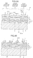
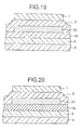
- a transparent electrode, an organic layer (particularly, the organic hole transfer layer, the hole block layer and the organic electron transfer layer), and a metallic electrode are laminated in this order on an optically transparent substrate.
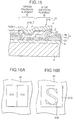
- Fig. 20 is a schematic cross sectional view showing an important part of a blue emission element 21B in a sixth embodiment according to the second aspect of the invention.
- BSB-BCN (having the formula (17)) was vapor deposited (vapor deposition rate: from 0.2 to 0.4 nm/sec) on the transparent electrode 5 as an electron transfer red emission material layer 32 at a thickness of 20 nm in the stripe pattern of 1.15 mm x 48.0 mm, which was an emission region of the ITO electrode 5, with changing to a mask 22c having 12 openings 23c having a stripe form having an area of 1.16 mm x 49 mm.
- Alq 3 (8-hydorxy quinoline aluminum having the formula (18)) was vapor deposited at a thickness of 40 nm as an electron transfer layer or an electron transfer emission layer 2.
- the specific constitution of the organic EL device 21 of this example is explained based on its production process.
- DMC2 (having the formula (19)) and Alq 3 (8-hydorxy quinoline aluminum having the formula (18)) was vapor deposited (vapor deposition rate: from 0.2 to 0.4 nm/sec) in such a manner that the molar ratio of DCM2 was from 0.5 to 1% on the transparent electrode 5 as an electron transfer red emission material layer 32 at a thickness of 20 nm in the stripe pattern of 1.15 mm x 48.0 mm, which was an emission region of the ITO electrode 5, with changing to a mask 22c having 12 openings 23c having a stripe form having an area of 1.16 mm x 49 mm.
- the organic EL device according to Example 3 of the invention is explained based on its production process.
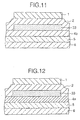
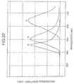
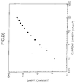
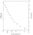
- Fig. 22 is a graph showing the spectral characteristics of the organic EL device according to Example 3 shown in Fig. 11.
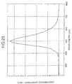
- the luminance was 1,400 cd/m 2 at a current density of 400 mA/cm 2 .
- the current did substantially not flow until a voltage of about 5 V, which gradually began to flow exceeding 5 V, and it suddenly flew exceeding 6 V. This means that it can be driven with a low voltage, and its threshold value voltage characteristics are good.
- the organic EL device according to Example 4 of the invention is explained based on its production process.
- the hole transfer layer can serve as an emission layer due to sufficient electron-hole recombination in the hole transfer layer by providing the hole block layer 33 between the hole transfer emission layer 4a and/or 4b and the electron transfer layer 2, so as to obtain stable emission with high efficiency.
- ⁇ -NPD ⁇ -naphtylphenyldiamine having the formula (13) functioning as a hole transfer layer or a hole transfer emission layer 4b was vapor deposited by a vacuum vapor deposition method under vacuum to a thickness of 50 nm at a vapor deposition rate of from 0.2 to 0.4 nm/sec.
- the mask was changed to a mask 22c having an opening 23c having an area of 1 mm x 2 mm, which covered a half of the emission region of 2 mm x 2 mm, bathocuproine (2,9-dimethyl-4,7-diphenyl-1,10-phenanthroline having the formula (3)) was vapor deposited at a vapor deposition rate of from 0.2 to 0.4 nm/sec as a hole block layer 33 at a thickness of 20 nm.
- the peak luminance converted to the direct current driven was 55,000 cd/m 2 at a current density of 5,500 mA/cm 2 , and a high luminance blue emission element having high performance sufficient to practical use could be produced.
- the mask was changed to 22a having an opening 23a of an area of 2 mm x 2 mm, Alq 3 (8-hydorxy quinoline aluminum having the formula (18)) functioning as an electron transfer layer or an electron transfer emission layer was vapor deposited at a thickness of 40 nm.
- LiF was vapor deposited at a thickness of about 0.5 nm, followed by further vapor depositing Al at a thickness of about 200 nm, to produce an organic electroluminescence device 21 emitting blue light and green light.
- the maximum emission wavelength in the emission region containing bathocuproine functioning as a hole block layer was 460 nm, and the coordinates on the CIE chromaticity coordinates were (0.155, 0.11), which resulted in good blue emission. It was apparent from the shape of the emission spectrum that it was emission from ⁇ -NPD. From the emission parts in the absence of bathocuproine, emission from Alq 3 as the electron transfer emission material was obtained, from which good green emission having the maximum emission wavelength of 520 nm and CIE (0.33, 0.55) was obtained.
- the device emitting blue light and green light thus produced was a device having a blue emission region having an emission region of 1 mm x 2 mm, which was emission from ⁇ -NPD, and a green emission region having an emission region of 1 mm x 2 mm, which was emission from Alq 3 , in the same emission region having an emission region of 2 mm x 2 mm.
- bathocuproine (2,9-dimethyl-4,7-diphenyl-1,10-phenanthroline having the formula (3)) was vapor deposited on the transparent electrode 5 as a hole block layer 33 at a thickness of 20 nm at a vapor deposition rate of from 0.2 to 0.4 nm/sec.
- the hole transfer layers and the electron transfer layers each comprise the common materials within each of the laminated bodies, in which the emission region is independently present in each of the hole transfer layer and the electron transfer layer, the laminated bodies for each of the colors of emission light can be easily produced with a simple process at a low cost.
- the common layers By forming the common layers on the whole surface of an organic pixel region by using a mask with a large opening, the film formation property and the step coverage property become good, and a leakage current between the cathode and the anode can be reduced.
Landscapes
- Physics & Mathematics (AREA)
- Chemical & Material Sciences (AREA)
- Engineering & Computer Science (AREA)
- Materials Engineering (AREA)
- Spectroscopy & Molecular Physics (AREA)
- Optics & Photonics (AREA)
- Inorganic Chemistry (AREA)
- Electroluminescent Light Sources (AREA)
Applications Claiming Priority (4)
| Application Number | Priority Date | Filing Date | Title |
|---|---|---|---|
| JP00298498A JP3852509B2 (ja) | 1998-01-09 | 1998-01-09 | 電界発光素子及びその製造方法 |
| JP298598 | 1998-01-09 | ||
| JP298498 | 1998-01-09 | ||
| JP00298598A JP4210872B2 (ja) | 1998-01-09 | 1998-01-09 | 電界発光素子及びその製造方法 |
Publications (3)
| Publication Number | Publication Date |
|---|---|
| EP0929104A2 true EP0929104A2 (de) | 1999-07-14 |
| EP0929104A3 EP0929104A3 (de) | 2003-03-26 |
| EP0929104B1 EP0929104B1 (de) | 2009-08-05 |
Family
ID=26336471
Family Applications (1)
| Application Number | Title | Priority Date | Filing Date |
|---|---|---|---|
| EP99100080A Expired - Lifetime EP0929104B1 (de) | 1998-01-09 | 1999-01-05 | Elektrolumineszente Vorrichtung und Herstellungsverfahren |
Country Status (4)
| Country | Link |
|---|---|
| US (1) | US6633122B2 (de) |
| EP (1) | EP0929104B1 (de) |
| KR (1) | KR100689163B1 (de) |
| DE (1) | DE69941200D1 (de) |
Cited By (8)
| Publication number | Priority date | Publication date | Assignee | Title |
|---|---|---|---|---|
| EP1191821A1 (de) * | 2000-09-25 | 2002-03-27 | Konica Corporation | Organisches Elektrolumineszenzelement und dafür verwendetes organisches Elektrolumineszenzmaterial |
| WO2002087288A1 (en) * | 2001-04-20 | 2002-10-31 | Elam-T Limited | Green light emitting electroluminescent material |
| EP1205528A4 (de) * | 2000-04-07 | 2004-10-27 | Sony Corp | Organisch lumineszierendes element und lumineszierender apparat dieses verwendend |
| US7052351B2 (en) * | 2002-12-31 | 2006-05-30 | Eastman Kodak Company | Using hole- or electron-blocking layers in color OLEDS |
| EP1234338A4 (de) * | 1999-11-26 | 2009-01-21 | Univ Princeton | Organische lichetmpfindliche optoelektronische anordnung mit einer exciton-blockierschicht |
| US7719014B2 (en) | 2001-12-28 | 2010-05-18 | Semiconductor Energy Laboratory Co., Ltd. | Light emitting device, method of manufacturing the same, and manufacturing apparatus therefor |
| WO2011141109A1 (de) * | 2010-05-11 | 2011-11-17 | Merck Patent Gmbh | Organische elektrolumineszenzvorrichtungen |
| EP3201961A1 (de) * | 2014-09-30 | 2017-08-09 | Novaled GmbH | Aktive oled-anzeige, verfahren zum betrieb einer aktiven oled-anzeige und verbindung |
Families Citing this family (17)
| Publication number | Priority date | Publication date | Assignee | Title |
|---|---|---|---|---|
| TW480722B (en) * | 1999-10-12 | 2002-03-21 | Semiconductor Energy Lab | Manufacturing method of electro-optical device |
| TW471011B (en) | 1999-10-13 | 2002-01-01 | Semiconductor Energy Lab | Thin film forming apparatus |
| US6867539B1 (en) * | 2000-07-12 | 2005-03-15 | 3M Innovative Properties Company | Encapsulated organic electronic devices and method for making same |
| US6906458B2 (en) * | 2000-08-11 | 2005-06-14 | Seiko Epson Corporation | Method for manufacturing organic EL device, organic EL device and electronic apparatus |
| KR100685914B1 (ko) * | 2000-09-05 | 2007-02-23 | 엘지.필립스 엘시디 주식회사 | 멀티 도메인 액정표시소자 및 그 제조방법 |
| US6739931B2 (en) * | 2000-09-18 | 2004-05-25 | Semiconductor Energy Laboratory Co., Ltd. | Display device and method of fabricating the display device |
| TW594617B (en) * | 2002-03-13 | 2004-06-21 | Sanyo Electric Co | Organic EL display panel and method for making the same |
| CN100557667C (zh) * | 2004-04-22 | 2009-11-04 | 株式会社半导体能源研究所 | 发光装置及其驱动方法 |
| GB0422391D0 (en) * | 2004-10-08 | 2004-11-10 | Cambridge Display Tech Ltd | Light emitting device |
| JP4595565B2 (ja) * | 2005-01-31 | 2010-12-08 | 株式会社デンソー | 自発光表示装置 |
| TWI361018B (en) * | 2005-04-18 | 2012-03-21 | Sony Corp | Display device and a method of manufacturing the s |
| US8258690B2 (en) * | 2005-10-11 | 2012-09-04 | Kuraray Co., Ltd. | High brightness inorganic electroluminescence device driven by direct current |
| JP2008027722A (ja) * | 2006-07-21 | 2008-02-07 | Sony Corp | 表示装置および表示装置の製造方法 |
| US8476844B2 (en) * | 2008-11-21 | 2013-07-02 | B/E Aerospace, Inc. | Light emitting diode (LED) lighting system providing precise color control |
| US7952106B2 (en) * | 2009-04-10 | 2011-05-31 | Everlight Electronics Co., Ltd. | Light emitting diode device having uniform current distribution and method for forming the same |
| US9929366B2 (en) * | 2013-05-17 | 2018-03-27 | Sumitomo Chemical Company, Limited | Organic EL element, and organic EL element manufacturing method |
| TWI731616B (zh) * | 2020-03-09 | 2021-06-21 | 財團法人紡織產業綜合研究所 | 電致發光線 |
Family Cites Families (10)
| Publication number | Priority date | Publication date | Assignee | Title |
|---|---|---|---|---|
| US5393614A (en) * | 1992-04-03 | 1995-02-28 | Pioneer Electronic Corporation | Organic electroluminescence device |
| EP0647694B1 (de) * | 1993-03-26 | 1999-09-15 | Sumitomo Electric Industries, Ltd. | Organische elektroluminineszente elementen |
| US5424560A (en) * | 1994-05-31 | 1995-06-13 | Motorola, Inc. | Integrated multicolor organic led array |
| US5693428A (en) * | 1995-02-06 | 1997-12-02 | Sanyo Electric Co., Ltd. | Organic electroluminescent device |
| US5837390A (en) * | 1995-05-10 | 1998-11-17 | Sony Corporation | Metal complex, method for producing the same and optical device |
| JP3672125B2 (ja) * | 1996-01-26 | 2005-07-13 | ソニー株式会社 | 光学的素子の製造方法 |
| DE69732548T2 (de) * | 1996-07-09 | 2006-01-12 | Sony Corp. | Elektrolumineszierende Anordnung |
| JPH1079297A (ja) * | 1996-07-09 | 1998-03-24 | Sony Corp | 電界発光素子 |
| US5949188A (en) * | 1996-12-18 | 1999-09-07 | Hage Gmbh & Co. Kg | Electroluminescent display device with continuous base electrode |
| JPH10183112A (ja) * | 1996-12-27 | 1998-07-14 | Sony Corp | 電界発光素子 |
-
1999
- 1999-01-05 DE DE69941200T patent/DE69941200D1/de not_active Expired - Lifetime
- 1999-01-05 EP EP99100080A patent/EP0929104B1/de not_active Expired - Lifetime
- 1999-01-07 US US09/226,854 patent/US6633122B2/en not_active Expired - Lifetime
- 1999-01-08 KR KR1019990000324A patent/KR100689163B1/ko not_active Expired - Fee Related
Cited By (16)
| Publication number | Priority date | Publication date | Assignee | Title |
|---|---|---|---|---|
| EP2400554A1 (de) * | 1999-11-26 | 2011-12-28 | The Trustees Of Princeton University | Organische lichtempfindliche optoelektronische Vorrichtung mit Exzitonblockierschicht |
| EP1234338A4 (de) * | 1999-11-26 | 2009-01-21 | Univ Princeton | Organische lichetmpfindliche optoelektronische anordnung mit einer exciton-blockierschicht |
| EP1205528A4 (de) * | 2000-04-07 | 2004-10-27 | Sony Corp | Organisch lumineszierendes element und lumineszierender apparat dieses verwendend |
| US7255935B2 (en) | 2000-04-07 | 2007-08-14 | Sony Corporation | Organic electroluminescent element and luminescent apparatus employing the same |
| US6723455B2 (en) | 2000-09-25 | 2004-04-20 | Konica Corporation | Organic electro-luminescent element and material of organic electro-luminescent element |
| EP1191821A1 (de) * | 2000-09-25 | 2002-03-27 | Konica Corporation | Organisches Elektrolumineszenzelement und dafür verwendetes organisches Elektrolumineszenzmaterial |
| WO2002087288A1 (en) * | 2001-04-20 | 2002-10-31 | Elam-T Limited | Green light emitting electroluminescent material |
| US9048203B2 (en) | 2001-12-28 | 2015-06-02 | Semiconductor Energy Laboratory Co., Ltd. | Light emitting device, method of manufacturing the same, and manufacturing apparatus therefor |
| US7982206B2 (en) | 2001-12-28 | 2011-07-19 | Semiconductor Energy Laboratory Co., Ltd. | Light emitting device, method of manufacturing the same, and manufacturing apparatus therefor |
| US7719014B2 (en) | 2001-12-28 | 2010-05-18 | Semiconductor Energy Laboratory Co., Ltd. | Light emitting device, method of manufacturing the same, and manufacturing apparatus therefor |
| US9450030B2 (en) | 2001-12-28 | 2016-09-20 | Semiconductor Energy Laboratory Co., Ltd. | Active matrix light-emitting device with overlapping electroluminescent layers |
| US10497755B2 (en) | 2001-12-28 | 2019-12-03 | Semiconductor Energy Laboratory Co., Ltd. | Light emitting device, method of manufacturing the same, and manufacturing apparatus therefor |
| US7052351B2 (en) * | 2002-12-31 | 2006-05-30 | Eastman Kodak Company | Using hole- or electron-blocking layers in color OLEDS |
| WO2011141109A1 (de) * | 2010-05-11 | 2011-11-17 | Merck Patent Gmbh | Organische elektrolumineszenzvorrichtungen |
| CN102884649A (zh) * | 2010-05-11 | 2013-01-16 | 默克专利有限公司 | 有机电致发光器件 |
| EP3201961A1 (de) * | 2014-09-30 | 2017-08-09 | Novaled GmbH | Aktive oled-anzeige, verfahren zum betrieb einer aktiven oled-anzeige und verbindung |
Also Published As
| Publication number | Publication date |
|---|---|
| EP0929104A3 (de) | 2003-03-26 |
| DE69941200D1 (de) | 2009-09-17 |
| KR100689163B1 (ko) | 2007-03-08 |
| US20020089282A1 (en) | 2002-07-11 |
| US6633122B2 (en) | 2003-10-14 |
| EP0929104B1 (de) | 2009-08-05 |
| KR19990067810A (ko) | 1999-08-25 |
Similar Documents
| Publication | Publication Date | Title |
|---|---|---|
| EP0929104B1 (de) | Elektrolumineszente Vorrichtung und Herstellungsverfahren | |
| EP1097981B1 (de) | Organische elektrolumineszente Vorrichtung | |
| JP3852509B2 (ja) | 電界発光素子及びその製造方法 | |
| US6010796A (en) | Electroluminescent device | |
| KR100903918B1 (ko) | 유기 전계발광 소자 및 표시 장치 | |
| US6582838B2 (en) | Red-emitting organic light emitting devices (OLED's) | |
| US20050214570A1 (en) | OLEDs doped with phosphorescent compounds | |
| JP2002334787A (ja) | 有機電界発光素子 | |
| KR100838094B1 (ko) | 유기 전계 발광 소자 및 이것을 사용한 발광장치 | |
| KR100751464B1 (ko) | 유기 전계 발광 소자 | |
| WO2004066315A2 (en) | Benzoxazinone and quinazolinone derivatives | |
| JP3672127B2 (ja) | 光学的素子の製造方法及び光学的素子 | |
| JPH11204259A (ja) | 電界発光素子 | |
| KR20020065389A (ko) | 유기 전계 발광 소자 및 표시장치 | |
| JP2000150152A (ja) | 有機エレクトロルミネッセンス表示装置 | |
| JP3129200B2 (ja) | 発光素子 | |
| JPH09232077A (ja) | 光学的素子及びその製造方法 | |
| KR100547056B1 (ko) | 전계발광소자 | |
| JP2000091077A (ja) | 有機電界発光素子 | |
| JP4210872B2 (ja) | 電界発光素子及びその製造方法 | |
| KR20050063659A (ko) | 백색 유기발광소자 | |
| JP2000150161A (ja) | 有機エレクトロルミネッセンス表示装置 | |
| KR19980081742A (ko) | 유기 전계발광 소자 | |
| JP2002208480A (ja) | 有機エレクトロルミネッセンス素子およびその製造方法 | |
| JP2006245011A (ja) | 電界発光素子及びその製造方法 |
Legal Events
| Date | Code | Title | Description |
|---|---|---|---|
| PUAI | Public reference made under article 153(3) epc to a published international application that has entered the european phase |
Free format text: ORIGINAL CODE: 0009012 |
|
| AK | Designated contracting states |
Kind code of ref document: A2 Designated state(s): AT BE CH CY DE DK ES FI FR GB GR IE IT LI LU MC NL PT SE |
|
| AX | Request for extension of the european patent |
Free format text: AL;LT;LV;MK;RO;SI |
|
| PUAL | Search report despatched |
Free format text: ORIGINAL CODE: 0009013 |
|
| AK | Designated contracting states |
Kind code of ref document: A3 Designated state(s): AT BE CH CY DE DK ES FI FR GB GR IE IT LI LU MC NL PT SE |
|
| AX | Request for extension of the european patent |
Extension state: AL LT LV MK RO SI |
|
| RIC1 | Information provided on ipc code assigned before grant |
Ipc: 7H 01L 27/00 B Ipc: 7H 01L 51/20 B Ipc: 7H 01L 27/15 A |
|
| 17P | Request for examination filed |
Effective date: 20030826 |
|
| AKX | Designation fees paid |
Designated state(s): DE FR GB |
|
| 17Q | First examination report despatched |
Effective date: 20061110 |
|
| RIC1 | Information provided on ipc code assigned before grant |
Ipc: H01L 27/15 20060101ALI20081215BHEP Ipc: H01L 51/52 20060101ALI20081215BHEP Ipc: H01L 27/32 20060101AFI20081215BHEP |
|
| GRAP | Despatch of communication of intention to grant a patent |
Free format text: ORIGINAL CODE: EPIDOSNIGR1 |
|
| GRAS | Grant fee paid |
Free format text: ORIGINAL CODE: EPIDOSNIGR3 |
|
| GRAA | (expected) grant |
Free format text: ORIGINAL CODE: 0009210 |
|
| AK | Designated contracting states |
Kind code of ref document: B1 Designated state(s): DE FR GB |
|
| REG | Reference to a national code |
Ref country code: GB Ref legal event code: FG4D |
|
| REF | Corresponds to: |
Ref document number: 69941200 Country of ref document: DE Date of ref document: 20090917 Kind code of ref document: P |
|
| PLBE | No opposition filed within time limit |
Free format text: ORIGINAL CODE: 0009261 |
|
| STAA | Information on the status of an ep patent application or granted ep patent |
Free format text: STATUS: NO OPPOSITION FILED WITHIN TIME LIMIT |
|
| 26N | No opposition filed |
Effective date: 20100507 |
|
| REG | Reference to a national code |
Ref country code: FR Ref legal event code: PLFP Year of fee payment: 17 |
|
| REG | Reference to a national code |
Ref country code: DE Ref legal event code: R082 Ref document number: 69941200 Country of ref document: DE Representative=s name: MUELLER HOFFMANN & PARTNER PATENTANWAELTE MBB, DE Ref country code: DE Ref legal event code: R081 Ref document number: 69941200 Country of ref document: DE Owner name: JOLED INC., JP Free format text: FORMER OWNER: SONY CORPORATION, TOKIO/TOKYO, JP |
|
| REG | Reference to a national code |
Ref country code: GB Ref legal event code: 732E Free format text: REGISTERED BETWEEN 20150806 AND 20150812 |
|
| REG | Reference to a national code |
Ref country code: FR Ref legal event code: PLFP Year of fee payment: 18 |
|
| REG | Reference to a national code |
Ref country code: FR Ref legal event code: TP Owner name: JOLED INC., JP Effective date: 20160112 |
|
| REG | Reference to a national code |
Ref country code: FR Ref legal event code: PLFP Year of fee payment: 19 |
|
| PGFP | Annual fee paid to national office [announced via postgrant information from national office to epo] |
Ref country code: FR Payment date: 20170120 Year of fee payment: 19 Ref country code: DE Payment date: 20170120 Year of fee payment: 19 |
|
| PGFP | Annual fee paid to national office [announced via postgrant information from national office to epo] |
Ref country code: GB Payment date: 20170119 Year of fee payment: 19 |
|
| REG | Reference to a national code |
Ref country code: DE Ref legal event code: R119 Ref document number: 69941200 Country of ref document: DE |
|
| GBPC | Gb: european patent ceased through non-payment of renewal fee |
Effective date: 20180105 |
|
| PG25 | Lapsed in a contracting state [announced via postgrant information from national office to epo] |
Ref country code: FR Free format text: LAPSE BECAUSE OF NON-PAYMENT OF DUE FEES Effective date: 20180131 Ref country code: DE Free format text: LAPSE BECAUSE OF NON-PAYMENT OF DUE FEES Effective date: 20180801 |
|
| REG | Reference to a national code |
Ref country code: FR Ref legal event code: ST Effective date: 20180928 |
|
| PG25 | Lapsed in a contracting state [announced via postgrant information from national office to epo] |
Ref country code: GB Free format text: LAPSE BECAUSE OF NON-PAYMENT OF DUE FEES Effective date: 20180105 |