EP0929105A2 - Metalgate-Submikron-MOS-Transistor und Verfahren zur Hertellung - Google Patents
Metalgate-Submikron-MOS-Transistor und Verfahren zur Hertellung Download PDFInfo
- Publication number
- EP0929105A2 EP0929105A2 EP99300130A EP99300130A EP0929105A2 EP 0929105 A2 EP0929105 A2 EP 0929105A2 EP 99300130 A EP99300130 A EP 99300130A EP 99300130 A EP99300130 A EP 99300130A EP 0929105 A2 EP0929105 A2 EP 0929105A2
- Authority
- EP
- European Patent Office
- Prior art keywords
- region
- layer
- gate
- mos transistor
- metal
- Prior art date
- Legal status (The legal status is an assumption and is not a legal conclusion. Google has not performed a legal analysis and makes no representation as to the accuracy of the status listed.)
- Withdrawn
Links
Images


Classifications
-
- H—ELECTRICITY
- H10—SEMICONDUCTOR DEVICES; ELECTRIC SOLID-STATE DEVICES NOT OTHERWISE PROVIDED FOR
- H10D—INORGANIC ELECTRIC SEMICONDUCTOR DEVICES
- H10D30/00—Field-effect transistors [FET]
- H10D30/01—Manufacture or treatment
- H10D30/021—Manufacture or treatment of FETs having insulated gates [IGFET]
- H10D30/0223—Manufacture or treatment of FETs having insulated gates [IGFET] having source and drain regions or source and drain extensions self-aligned to sides of the gate
- H10D30/0227—Manufacture or treatment of FETs having insulated gates [IGFET] having source and drain regions or source and drain extensions self-aligned to sides of the gate having both lightly-doped source and drain extensions and source and drain regions self-aligned to the sides of the gate, e.g. lightly-doped drain [LDD] MOSFET or double-diffused drain [DDD] MOSFET
-
- H—ELECTRICITY
- H10—SEMICONDUCTOR DEVICES; ELECTRIC SOLID-STATE DEVICES NOT OTHERWISE PROVIDED FOR
- H10D—INORGANIC ELECTRIC SEMICONDUCTOR DEVICES
- H10D84/00—Integrated devices formed in or on semiconductor substrates that comprise only semiconducting layers, e.g. on Si wafers or on GaAs-on-Si wafers
-
- H—ELECTRICITY
- H10—SEMICONDUCTOR DEVICES; ELECTRIC SOLID-STATE DEVICES NOT OTHERWISE PROVIDED FOR
- H10D—INORGANIC ELECTRIC SEMICONDUCTOR DEVICES
- H10D64/00—Electrodes of devices having potential barriers
- H10D64/01—Manufacture or treatment
- H10D64/013—Manufacture or treatment of electrodes having a conductor capacitively coupled to a semiconductor by an insulator
- H10D64/01302—Manufacture or treatment of electrodes having a conductor capacitively coupled to a semiconductor by an insulator the insulator being formed after the semiconductor body, the semiconductor being silicon
- H10D64/01304—Manufacture or treatment of electrodes having a conductor capacitively coupled to a semiconductor by an insulator the insulator being formed after the semiconductor body, the semiconductor being silicon characterised by the conductor
- H10D64/01318—Manufacture or treatment of electrodes having a conductor capacitively coupled to a semiconductor by an insulator the insulator being formed after the semiconductor body, the semiconductor being silicon characterised by the conductor the conductor comprising a layer of alloy material, compound material or organic material contacting the insulator, e.g. TiN
- H10D64/0132—Manufacture or treatment of electrodes having a conductor capacitively coupled to a semiconductor by an insulator the insulator being formed after the semiconductor body, the semiconductor being silicon characterised by the conductor the conductor comprising a layer of alloy material, compound material or organic material contacting the insulator, e.g. TiN the conductor being a metallic silicide
-
- H—ELECTRICITY
- H10—SEMICONDUCTOR DEVICES; ELECTRIC SOLID-STATE DEVICES NOT OTHERWISE PROVIDED FOR
- H10D—INORGANIC ELECTRIC SEMICONDUCTOR DEVICES
- H10D64/00—Electrodes of devices having potential barriers
- H10D64/01—Manufacture or treatment
- H10D64/017—Manufacture or treatment using dummy gates in processes wherein at least parts of the final gates are self-aligned to the dummy gates, i.e. replacement gate processes
-
- H—ELECTRICITY
- H10—SEMICONDUCTOR DEVICES; ELECTRIC SOLID-STATE DEVICES NOT OTHERWISE PROVIDED FOR
- H10D—INORGANIC ELECTRIC SEMICONDUCTOR DEVICES
- H10D64/00—Electrodes of devices having potential barriers
- H10D64/60—Electrodes characterised by their materials
- H10D64/66—Electrodes having a conductor capacitively coupled to a semiconductor by an insulator, e.g. MIS electrodes
- H10D64/667—Electrodes having a conductor capacitively coupled to a semiconductor by an insulator, e.g. MIS electrodes the conductor comprising a layer of alloy material, compound material or organic material contacting the insulator, e.g. TiN workfunction layers
- H10D64/668—Electrodes having a conductor capacitively coupled to a semiconductor by an insulator, e.g. MIS electrodes the conductor comprising a layer of alloy material, compound material or organic material contacting the insulator, e.g. TiN workfunction layers the layer being a silicide, e.g. TiSi2
-
- H—ELECTRICITY
- H10—SEMICONDUCTOR DEVICES; ELECTRIC SOLID-STATE DEVICES NOT OTHERWISE PROVIDED FOR
- H10D—INORGANIC ELECTRIC SEMICONDUCTOR DEVICES
- H10D84/00—Integrated devices formed in or on semiconductor substrates that comprise only semiconducting layers, e.g. on Si wafers or on GaAs-on-Si wafers
- H10D84/01—Manufacture or treatment
- H10D84/0123—Integrating together multiple components covered by H10D12/00 or H10D30/00, e.g. integrating multiple IGBTs
- H10D84/0126—Integrating together multiple components covered by H10D12/00 or H10D30/00, e.g. integrating multiple IGBTs the components including insulated gates, e.g. IGFETs
- H10D84/0165—Integrating together multiple components covered by H10D12/00 or H10D30/00, e.g. integrating multiple IGBTs the components including insulated gates, e.g. IGFETs the components including complementary IGFETs, e.g. CMOS devices
- H10D84/0172—Manufacturing their gate conductors
- H10D84/0179—Manufacturing their gate conductors the gate conductors having different shapes or dimensions
-
- H—ELECTRICITY
- H10—SEMICONDUCTOR DEVICES; ELECTRIC SOLID-STATE DEVICES NOT OTHERWISE PROVIDED FOR
- H10D—INORGANIC ELECTRIC SEMICONDUCTOR DEVICES
- H10D84/00—Integrated devices formed in or on semiconductor substrates that comprise only semiconducting layers, e.g. on Si wafers or on GaAs-on-Si wafers
- H10D84/01—Manufacture or treatment
- H10D84/02—Manufacture or treatment characterised by using material-based technologies
- H10D84/03—Manufacture or treatment characterised by using material-based technologies using Group IV technology, e.g. silicon technology or silicon-carbide [SiC] technology
- H10D84/038—Manufacture or treatment characterised by using material-based technologies using Group IV technology, e.g. silicon technology or silicon-carbide [SiC] technology using silicon technology, e.g. SiGe
-
- H—ELECTRICITY
- H10—SEMICONDUCTOR DEVICES; ELECTRIC SOLID-STATE DEVICES NOT OTHERWISE PROVIDED FOR
- H10W—GENERIC PACKAGES, INTERCONNECTIONS, CONNECTORS OR OTHER CONSTRUCTIONAL DETAILS OF DEVICES COVERED BY CLASS H10
- H10W20/00—Interconnections in chips, wafers or substrates
- H10W20/01—Manufacture or treatment
- H10W20/031—Manufacture or treatment of conductive parts of the interconnections
- H10W20/0698—Local interconnections
-
- H—ELECTRICITY
- H10—SEMICONDUCTOR DEVICES; ELECTRIC SOLID-STATE DEVICES NOT OTHERWISE PROVIDED FOR
- H10W—GENERIC PACKAGES, INTERCONNECTIONS, CONNECTORS OR OTHER CONSTRUCTIONAL DETAILS OF DEVICES COVERED BY CLASS H10
- H10W20/00—Interconnections in chips, wafers or substrates
- H10W20/40—Interconnections external to wafers or substrates, e.g. back-end-of-line [BEOL] metallisations or vias connecting to gate electrodes
-
- H—ELECTRICITY
- H10—SEMICONDUCTOR DEVICES; ELECTRIC SOLID-STATE DEVICES NOT OTHERWISE PROVIDED FOR
- H10D—INORGANIC ELECTRIC SEMICONDUCTOR DEVICES
- H10D64/00—Electrodes of devices having potential barriers
- H10D64/20—Electrodes characterised by their shapes, relative sizes or dispositions
- H10D64/27—Electrodes not carrying the current to be rectified, amplified, oscillated or switched, e.g. gates
- H10D64/311—Gate electrodes for field-effect devices
- H10D64/411—Gate electrodes for field-effect devices for FETs
- H10D64/511—Gate electrodes for field-effect devices for FETs for IGFETs
- H10D64/517—Gate electrodes for field-effect devices for FETs for IGFETs characterised by the conducting layers
- H10D64/518—Gate electrodes for field-effect devices for FETs for IGFETs characterised by the conducting layers characterised by their lengths or sectional shapes
-
- H—ELECTRICITY
- H10—SEMICONDUCTOR DEVICES; ELECTRIC SOLID-STATE DEVICES NOT OTHERWISE PROVIDED FOR
- H10W—GENERIC PACKAGES, INTERCONNECTIONS, CONNECTORS OR OTHER CONSTRUCTIONAL DETAILS OF DEVICES COVERED BY CLASS H10
- H10W20/00—Interconnections in chips, wafers or substrates
- H10W20/01—Manufacture or treatment
- H10W20/031—Manufacture or treatment of conductive parts of the interconnections
- H10W20/069—Manufacture or treatment of conductive parts of the interconnections by forming self-aligned vias or self-aligned contact plugs
Definitions
- the invention relates to MOS semiconductor devices and fabrication methods therefor, and specifically to a MOS transistor having an exceptionally thin metal gate therein.
- MOS metal-oxide-semiconductor
- metal gate fabrication processes are complicated and pose difficult structural considerations during the fabrication of self-aligned components. For instance, copper makes an ideal metal gate, but it has poor adhesive characteristics as a thin film. Aluminum may also be used as a metal gate, but it is subject to electromigration problems.
- the MOS transistor of the invention is formed on a single crystal silicon substrate doped to form a conductive layer of a first type, and includes: an active region formed on a substrate; a source region and a drain region located in the active region, doped to form conductive channels of a second type; a metal gate region located in the active region between the source region and the drain region, wherein the metal gate has a width of less than one micron; a gate oxide region located over the gate region; an oxide region located over the structure; and a source electrode, a gate electrode and a drain electrode, each connected to their respective regions, and each formed of a combination of a contact metal and an electrode metaL
- An alternate embodiment includes a pair of MOS transistors which have an interconnect between their gate electrodes and the drain electrode of one transistor and the drain electrode of the other transistor.
- An object of the invention is to provide a cost effective method for manufacturing a metal gate sub-micron channel length MOS integrated circuit. Another object of the invention is to provide a metal gate sub-micron channel length MOS integrated circuit which has a high current density.
- Figs. 1-6 depict successive steps in the fabrication of the metal gate sub-micron MOS transistor of the invention.
- Fig. 7 is a front sectional elevation of a MOS IC constructed according to the invention.
- Figs. 8-10 depict successive steps in fabrication of an alternate embodiment of the metal gate sub-micron MOS transistor of the invention.
- Fig. 11 is a front sectional elevation of an alternate embodiment of a MOS IC constructed according to the invention.
- MOS metal gate sub-micron metal-oxide semiconductor
- Sub-micron means that the metal gate used in the structure of the invention is less than 1000 nm in width. It will be appreciated that any suitable integrated circuit interconnect material, which includes all refractory metals, the most common of which is aluminum, may be used. In the examples provided herein, an n - channel MOS transistor will be used, although the structure and fabrication process may also be used to provide a p - channel MOS transistor and complimentary metal-oxide semiconductor (CMOS) integration, provided proper doping of the silicon substrate is initially performed.
- CMOS complimentary metal-oxide semiconductor
- a silicon substrate 10 is provided, which will be used to form a MOS transistor 11.
- Substrate 10 has been processed to form an oxide insulation boundary about an active region, shown as boundaries 12, 14, over a p - silicon substrate, defining a device area 15. It will be understood by those of skill in the art that the silicon substrate is treated to prepare a p - well by doping impurities of a first type, thereby forming a conductive channel of a first type, and to have the threshold voltage adjustments suitable for fabrication of the device of the invention.
- p - substrate 10 may be formed by single boron ion implantation at an energy level of 30 keV to 80 keV and a dose of 1.0 ⁇ 10 12 cm -2 to 1.0 ⁇ 10 14 cm -2 , followed by thermal diffusion.
- p - substrate 10 may be formed by multiple boron ion implantation, followed by thermal diffusion.
- a gate oxide region 16 has been formed to a thickness of not greater than 10 nm.
- This oxide region may be formed by conventional or rapid thermal oxidation, chemical vapor deposition (CVD) or other suitable techniques.
- a layer of polysilicon material 18 may be deposited.
- Layer 18 has a thickness of between 10 nm and 50 nm. This layer is deposited to protect the gate oxide during the subsequent processing, and while this layer may be omitted, or replaced with any type of barrier or metal layer, it provides an effective, efficient way to protect what will become the gate region.
- a layer of silicon nitride (Si 3 N 4 ) 20 may be deposited to a thickness of between , 300 nm and 700 nm.
- Appropriate photoresist material is applied and the nitride and polysilicon layers are plasma etched, resulting in a polysilicon region 18 and a nitride plug 20, as shown in Fig. 2.
- the etching process may be a one or two step process. In the two step process, the first etching process stops at gate oxide layer 16. A subsequent etching step removes the gate oxide layer on either side of plug 20 and region 18. In the one step process, etching removes all of the extraneous material down to the p - silicon substrate 10.
- Nitride plug 20 polysilicon region 18 and the remaining oxide layer 16 are referred to herein as the stacked layers.
- Appropriate ions are implanted to form LDD regions (not shown). Such implantation also defines, by default, a gate region 25 in the p - silicon substrate. Gate region 25 is also referred to herein as a conductive channel of a first type.
- Source region 22 and drain region 24 are formed by any well known processes to form a lightly doped conductive region. Such processes include LDD, MDD, and HALO structure.
- a layer of silicon oxide is formed by CVD to a thickness of between 50 nm and 200 nm over polysilicon region 18 and nitride plug 20. This oxide layer is plasma etched to form an oxide spacer 26, 28, as shown in Fig. 3, at the sidewalls of nitride plug 20. Any other insulator, other than silicon nitride, may also be used for this step of the process if desired.
- Appropriate ions are implanted to form source region 22 and drain region 24 and are defused or activated.
- the source and drain regions are referred to herein as conductive channels of a second type, which are n + channels, and the impurities implanted in the substrate are referred to doping impurities of a second type.
- the LDD may be done by phosphorous (P) or arsenic (As) ion implantation at an energy no higher than 70 keV (P) or 140 keV (As), and a dose of between 1.0 ⁇ 10 13 cm -2 to 5.0 ⁇ 10 14 cm -2 .
- the n + layer may be formed by As ion implantation at an energy level of between 10 keV and 80 keV, at a does of between 1.0 ⁇ 10 15 cm -2 to 5.0 ⁇ 10 15 cm -2 .
- a salicide process may also be performed if desired.
- the salicide (self-aligned silicide) formation process includes formation of a layer of Ti or Co to a thickness of between 30 nm to 60 nm, preferably by CVD, in a nitrogen atmosphere at 500°C to 650° C for Ti, or 450° C to 600° C for Co. The excess Ti or Co is removed by etching, and rapid thermal annealed (RTA) in nitrogen at 700° C to 850° C for Ti or 650° C to 800° C for Co.
- RTA rapid thermal annealed
- silicon dioxide is again added by CVD to a thickness of about 15 to 2 times that of silicon nitride plug 20, resulting in oxide regions 30, 32.
- the structure is planarized, preferably by a chemical-mechanical polishing process, to expose the upper surface of silicon nitride plug 20.
- the planarization by CMP will provide a surface having a uniformity of approximately 5%.
- the structure is covered with photoresist to protect specified areas of oxide regions 30, 32.
- Trenches, 34, 36, are formed for source and drain electrodes, respectively.
- Via holes, 38, 40 are formed for additional portions of the source and drain electrodes, respectively, to enable to electrodes to join to their respective conductive regions.
- This portion of the method may involve a conventional two-mask process, a double resist process, or a half-tone mask process.
- the photoresist is stripped off of the structure.
- the next step of the process includes a wet etch in phosphoric acid (H 3 PO 4 ) solution, or any suitable selective etchant which will remove silicon nitride plug 20, but which will not etch the oxide regions 30, 32, silicon region 10, or polysilicon layer 18.
- H 3 PO 4 phosphoric acid
- a layer of contact metal such as Ti, Ta, TaN, TaSiN, W, WN, WSiN, or Re, and a barrier metal such as TiN, is deposited by CVD, and depicted at 44.
- metal material such as copper
- MOCVD or other CVD, PVD, and sputtering processes, and forms a region 46.
- other metal such as aluminum or a refractory metal, may also be used.
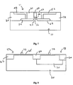
- Metal region 46 and contact metal 44 are then planar etched, wherein the etching stops at oxide regions 30, 32, resulting, and now referring to Fig.
- a source electrode 48, and a gate electrode 50, and a drain electrode 52 in the formation of a source electrode 48, and a gate electrode 50, and a drain electrode 52.
- a CMP process is preferable for this planar etching.
- the structure is annealed at a temperature of between 500° C and 900° C for one-half hour, to form a good contact between the electrodes and their conductive channels.
- Polysilicon layer 18 will be converted into silicide 54 during the annealing process.
- the conventional polysilicon gate is displaced by metal gate electrode 50.
- the gate length of the device is determined by the width of gate electrode 50. It will be appreciated that the structure is three-dimensional, and has a depth (into the page of the drawings) approximately equal to its width, forming a generally rectangular active region for the gate, and forming other three-dimensional strutures for the other parts of the transistor.
- the materials used for the source, gate, and drain electrodes are all identical and are fabricated simultaneously during a first level interconnect.
- the gate is self-aligned with the source and drain region. While an n - channel MOS transistor has been used as an example, it will be understood that the same process, with proper replacement in silicon dopant, is applicable to p - channel transistors and for CMOS IC fabrication.
- the doping density of the channel regions is low to yield high drive current and low substrate bias effect.
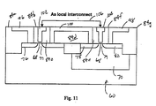
- An alternative process and structure may be formed with a local interconnect between a pair of MOS transistors, 56, 58.
- a substrate 60 is properly doped to form a substrate of a proper polarity, in this case a p - substrate.
- Silicon dioxide insulating regions 62, 64, and 66 are formed, and a layer of silicon dioxide 68 is thermally grown or is deposited by CVD.
- an n - well 70 is also formed, which is referred to as a conductive channel of a third type, by implanting doping impurities of a third type into the substrate, namely, phosphorous, at an energy level of 50 keV to 180 keV and a dose of 1.0 ⁇ 10 12 cm -2 to 5.0 ⁇ 10 13 cm -2 .
- the gate electrodes of both n - channel 72 and p - channel 74 are made as previously described, i.e., by the formation of a silicon nitride replacement plug.
- the LDD, and p + and n + are implanted using conventional processes.
- the p - channel LDD may be formed by BF 2 at an energy of less than 100 keV and a dose of between 1.0 ⁇ 10 13 cm -2 to 5.0 ⁇ 10 14 cm -2 .
- the p - channel source and drain regions may be formed by implantation of BF 2 ions at an energy of between 10 keV to 60 keV and a dose of 1.0 ⁇ 10 15 cm -2 to 5.0 ⁇ 10 15 cm -2 .
- the optional salicide region is formed as previously described. Source regions 76, 82, and drain regions 80, 78 are formed.
- Oxide layer 84 should be approximately three times thicker than the thickness of barrier metal 72/74. (Drawings not to scale.)
- the surface of oxide layer 84 is planarized, as by chemical-mechanical polishing to the configuration depicted in Fig. 9.
- the oxide layer is covered with photoresist and is Damascene trenched and contact etched to the configuration depicted in Fig. 10, resulting in a trench and via hole 86 for a source electrode which will connect to source 76, a trench/via hole 88 which will provide a region for a source electrode which will connect to source region 82 and a trench/via hole 90, which will provide an electrode connected to drain region 80 and to drain region 78. Additionally, the oxide layer is etched away to provide holes 92 and 94 which will provide room for gate electrodes, which also include an interconnect area, which is out of the plane of the drawing, which will connect to gates 77, 79, respectively.
- a second barrier metal is deposited by CVD, as was explained in connection with Fig. 6.
- the second barrier material may be TiN, or WN, or other suitable barrier metal which will provide good ohmic contact to both n + and p + silicon, and which are selected to prevent metal diffusion into the silicon.
- Metal is then deposited over the structure by CVD or sputtering, which metal may be Cu, Mo, or W, or Al, or other suitable metaL
- the structure is then chemically-mechanically polished to the level of the oxide regions, resulting in the configuration depicted in Fig. 11.
- a first, nMOST source electrode 96 is formed as is a second, pMOST source electrode 98.
- An interconnect electrode 100 connects to nMOST drain region 80 and pMOST drain region 78.
- Gate electrodes 102, 104 are joined by a local interconnect 106.
- the integrated circuit formed hereby is characterized by a high drive current and a low substrate bias effect.
- the structure is simple and is a cost-effective method for forming the metal gate sub-micron MOS transistor.
Landscapes
- Insulated Gate Type Field-Effect Transistor (AREA)
- Metal-Oxide And Bipolar Metal-Oxide Semiconductor Integrated Circuits (AREA)
- Electrodes Of Semiconductors (AREA)
- Thin Film Transistor (AREA)
Applications Claiming Priority (2)
| Application Number | Priority Date | Filing Date | Title |
|---|---|---|---|
| US09/004,991 US6274421B1 (en) | 1998-01-09 | 1998-01-09 | Method of making metal gate sub-micron MOS transistor |
| US4991 | 1998-01-09 |
Publications (2)
| Publication Number | Publication Date |
|---|---|
| EP0929105A2 true EP0929105A2 (de) | 1999-07-14 |
| EP0929105A3 EP0929105A3 (de) | 1999-12-22 |
Family
ID=21713564
Family Applications (1)
| Application Number | Title | Priority Date | Filing Date |
|---|---|---|---|
| EP99300130A Withdrawn EP0929105A3 (de) | 1998-01-09 | 1999-01-08 | Metalgate-Submikron-MOS-Transistor und Verfahren zur Hertellung |
Country Status (5)
| Country | Link |
|---|---|
| US (3) | US6274421B1 (de) |
| EP (1) | EP0929105A3 (de) |
| JP (1) | JPH11224949A (de) |
| KR (1) | KR100352715B1 (de) |
| TW (1) | TW434901B (de) |
Cited By (4)
| Publication number | Priority date | Publication date | Assignee | Title |
|---|---|---|---|---|
| WO2001045156A1 (en) * | 1999-12-17 | 2001-06-21 | Koninklijke Philips Electronics N.V. | A method of manufacturing a semiconductor device |
| US6607950B2 (en) | 2000-03-30 | 2003-08-19 | Interuniversitair Microelektronic Centrum (Imec) | MIS transistors with a metal gate and high-k dielectric and method of forming |
| WO2004012256A1 (en) * | 2002-07-31 | 2004-02-05 | Advanced Micro Devices, Inc. | Process for manufacturing mosfets using amorphous carbon replacement gate and structures formed in accordance therewith |
| EP1496541A1 (de) | 2003-07-10 | 2005-01-12 | Samsung Electronics Co., Ltd. | Methode zur Herstellung eines MOS Transistors |
Families Citing this family (90)
| Publication number | Priority date | Publication date | Assignee | Title |
|---|---|---|---|---|
| KR100624961B1 (ko) * | 1999-10-20 | 2006-09-19 | 주식회사 하이닉스반도체 | 메탈 게이트를 채용한 트랜지스터 제조방법 |
| US7008832B1 (en) | 2000-07-20 | 2006-03-07 | Advanced Micro Devices, Inc. | Damascene process for a T-shaped gate electrode |
| US6417084B1 (en) * | 2000-07-20 | 2002-07-09 | Advanced Micro Devices, Inc. | T-gate formation using a modified conventional poly process |
| US6509282B1 (en) | 2001-11-26 | 2003-01-21 | Advanced Micro Devices, Inc. | Silicon-starved PECVD method for metal gate electrode dielectric spacer |
| JP2004152790A (ja) * | 2002-10-28 | 2004-05-27 | Toshiba Corp | 半導体装置、及び、半導体装置の製造方法 |
| US7388259B2 (en) * | 2002-11-25 | 2008-06-17 | International Business Machines Corporation | Strained finFET CMOS device structures |
| US7078298B2 (en) * | 2003-05-20 | 2006-07-18 | Sharp Laboratories Of America, Inc. | Silicon-on-nothing fabrication process |
| US6887798B2 (en) | 2003-05-30 | 2005-05-03 | International Business Machines Corporation | STI stress modification by nitrogen plasma treatment for improving performance in small width devices |
| US7410846B2 (en) * | 2003-09-09 | 2008-08-12 | International Business Machines Corporation | Method for reduced N+ diffusion in strained Si on SiGe substrate |
| US6890808B2 (en) * | 2003-09-10 | 2005-05-10 | International Business Machines Corporation | Method and structure for improved MOSFETs using poly/silicide gate height control |
| US6887751B2 (en) * | 2003-09-12 | 2005-05-03 | International Business Machines Corporation | MOSFET performance improvement using deformation in SOI structure |
| US7170126B2 (en) | 2003-09-16 | 2007-01-30 | International Business Machines Corporation | Structure of vertical strained silicon devices |
| US7144767B2 (en) * | 2003-09-23 | 2006-12-05 | International Business Machines Corporation | NFETs using gate induced stress modulation |
| US7119403B2 (en) * | 2003-10-16 | 2006-10-10 | International Business Machines Corporation | High performance strained CMOS devices |
| US7037770B2 (en) * | 2003-10-20 | 2006-05-02 | International Business Machines Corporation | Method of manufacturing strained dislocation-free channels for CMOS |
| US7303949B2 (en) * | 2003-10-20 | 2007-12-04 | International Business Machines Corporation | High performance stress-enhanced MOSFETs using Si:C and SiGe epitaxial source/drain and method of manufacture |
| US7129126B2 (en) * | 2003-11-05 | 2006-10-31 | International Business Machines Corporation | Method and structure for forming strained Si for CMOS devices |
| US7015082B2 (en) * | 2003-11-06 | 2006-03-21 | International Business Machines Corporation | High mobility CMOS circuits |
| US7029964B2 (en) * | 2003-11-13 | 2006-04-18 | International Business Machines Corporation | Method of manufacturing a strained silicon on a SiGe on SOI substrate |
| US7122849B2 (en) | 2003-11-14 | 2006-10-17 | International Business Machines Corporation | Stressed semiconductor device structures having granular semiconductor material |
| US7247534B2 (en) | 2003-11-19 | 2007-07-24 | International Business Machines Corporation | Silicon device on Si:C-OI and SGOI and method of manufacture |
| US7198995B2 (en) | 2003-12-12 | 2007-04-03 | International Business Machines Corporation | Strained finFETs and method of manufacture |
| US7247912B2 (en) * | 2004-01-05 | 2007-07-24 | International Business Machines Corporation | Structures and methods for making strained MOSFETs |
| US7381609B2 (en) | 2004-01-16 | 2008-06-03 | International Business Machines Corporation | Method and structure for controlling stress in a transistor channel |
| US7202132B2 (en) | 2004-01-16 | 2007-04-10 | International Business Machines Corporation | Protecting silicon germanium sidewall with silicon for strained silicon/silicon germanium MOSFETs |
| US7118999B2 (en) * | 2004-01-16 | 2006-10-10 | International Business Machines Corporation | Method and apparatus to increase strain effect in a transistor channel |
| US7923782B2 (en) * | 2004-02-27 | 2011-04-12 | International Business Machines Corporation | Hybrid SOI/bulk semiconductor transistors |
| US7205206B2 (en) * | 2004-03-03 | 2007-04-17 | International Business Machines Corporation | Method of fabricating mobility enhanced CMOS devices |
| US7504693B2 (en) * | 2004-04-23 | 2009-03-17 | International Business Machines Corporation | Dislocation free stressed channels in bulk silicon and SOI CMOS devices by gate stress engineering |
| US7223994B2 (en) * | 2004-06-03 | 2007-05-29 | International Business Machines Corporation | Strained Si on multiple materials for bulk or SOI substrates |
| US7037794B2 (en) * | 2004-06-09 | 2006-05-02 | International Business Machines Corporation | Raised STI process for multiple gate ox and sidewall protection on strained Si/SGOI structure with elevated source/drain |
| US7227205B2 (en) | 2004-06-24 | 2007-06-05 | International Business Machines Corporation | Strained-silicon CMOS device and method |
| TWI463526B (zh) | 2004-06-24 | 2014-12-01 | 萬國商業機器公司 | 改良具應力矽之cmos元件的方法及以該方法製備而成的元件 |
| US7288443B2 (en) * | 2004-06-29 | 2007-10-30 | International Business Machines Corporation | Structures and methods for manufacturing p-type MOSFET with graded embedded silicon-germanium source-drain and/or extension |
| US7217949B2 (en) | 2004-07-01 | 2007-05-15 | International Business Machines Corporation | Strained Si MOSFET on tensile-strained SiGe-on-insulator (SGOI) |
| US6991998B2 (en) * | 2004-07-02 | 2006-01-31 | International Business Machines Corporation | Ultra-thin, high quality strained silicon-on-insulator formed by elastic strain transfer |
| US7384829B2 (en) | 2004-07-23 | 2008-06-10 | International Business Machines Corporation | Patterned strained semiconductor substrate and device |
| CN100539035C (zh) * | 2004-09-10 | 2009-09-09 | 中芯国际集成电路制造(上海)有限公司 | 半导体集成电路硅单晶片衬底背面氮化硅层的新腐蚀方法 |
| US7338907B2 (en) * | 2004-10-04 | 2008-03-04 | Sharp Laboratories Of America, Inc. | Selective etching processes of silicon nitride and indium oxide thin films for FeRAM device applications |
| US7238565B2 (en) | 2004-12-08 | 2007-07-03 | International Business Machines Corporation | Methodology for recovery of hot carrier induced degradation in bipolar devices |
| US7262087B2 (en) * | 2004-12-14 | 2007-08-28 | International Business Machines Corporation | Dual stressed SOI substrates |
| US7173312B2 (en) * | 2004-12-15 | 2007-02-06 | International Business Machines Corporation | Structure and method to generate local mechanical gate stress for MOSFET channel mobility modification |
| US7274084B2 (en) * | 2005-01-12 | 2007-09-25 | International Business Machines Corporation | Enhanced PFET using shear stress |
| US20060160317A1 (en) * | 2005-01-18 | 2006-07-20 | International Business Machines Corporation | Structure and method to enhance stress in a channel of cmos devices using a thin gate |
| US7432553B2 (en) * | 2005-01-19 | 2008-10-07 | International Business Machines Corporation | Structure and method to optimize strain in CMOSFETs |
| US7220626B2 (en) * | 2005-01-28 | 2007-05-22 | International Business Machines Corporation | Structure and method for manufacturing planar strained Si/SiGe substrate with multiple orientations and different stress levels |
| US7256081B2 (en) * | 2005-02-01 | 2007-08-14 | International Business Machines Corporation | Structure and method to induce strain in a semiconductor device channel with stressed film under the gate |
| US7224033B2 (en) | 2005-02-15 | 2007-05-29 | International Business Machines Corporation | Structure and method for manufacturing strained FINFET |
| US7545004B2 (en) * | 2005-04-12 | 2009-06-09 | International Business Machines Corporation | Method and structure for forming strained devices |
| US7544577B2 (en) * | 2005-08-26 | 2009-06-09 | International Business Machines Corporation | Mobility enhancement in SiGe heterojunction bipolar transistors |
| US7202513B1 (en) | 2005-09-29 | 2007-04-10 | International Business Machines Corporation | Stress engineering using dual pad nitride with selective SOI device architecture |
| US20070096170A1 (en) * | 2005-11-02 | 2007-05-03 | International Business Machines Corporation | Low modulus spacers for channel stress enhancement |
| US7655511B2 (en) | 2005-11-03 | 2010-02-02 | International Business Machines Corporation | Gate electrode stress control for finFET performance enhancement |
| US7785950B2 (en) * | 2005-11-10 | 2010-08-31 | International Business Machines Corporation | Dual stress memory technique method and related structure |
| US7348638B2 (en) * | 2005-11-14 | 2008-03-25 | International Business Machines Corporation | Rotational shear stress for charge carrier mobility modification |
| US7709317B2 (en) | 2005-11-14 | 2010-05-04 | International Business Machines Corporation | Method to increase strain enhancement with spacerless FET and dual liner process |
| US7564081B2 (en) | 2005-11-30 | 2009-07-21 | International Business Machines Corporation | finFET structure with multiply stressed gate electrode |
| US7863197B2 (en) | 2006-01-09 | 2011-01-04 | International Business Machines Corporation | Method of forming a cross-section hourglass shaped channel region for charge carrier mobility modification |
| US7776695B2 (en) * | 2006-01-09 | 2010-08-17 | International Business Machines Corporation | Semiconductor device structure having low and high performance devices of same conductive type on same substrate |
| US7635620B2 (en) * | 2006-01-10 | 2009-12-22 | International Business Machines Corporation | Semiconductor device structure having enhanced performance FET device |
| US20070158743A1 (en) * | 2006-01-11 | 2007-07-12 | International Business Machines Corporation | Thin silicon single diffusion field effect transistor for enhanced drive performance with stress film liners |
| US7691698B2 (en) * | 2006-02-21 | 2010-04-06 | International Business Machines Corporation | Pseudomorphic Si/SiGe/Si body device with embedded SiGe source/drain |
| US8461009B2 (en) * | 2006-02-28 | 2013-06-11 | International Business Machines Corporation | Spacer and process to enhance the strain in the channel with stress liner |
| US7521307B2 (en) | 2006-04-28 | 2009-04-21 | International Business Machines Corporation | CMOS structures and methods using self-aligned dual stressed layers |
| US7615418B2 (en) * | 2006-04-28 | 2009-11-10 | International Business Machines Corporation | High performance stress-enhance MOSFET and method of manufacture |
| US7608489B2 (en) * | 2006-04-28 | 2009-10-27 | International Business Machines Corporation | High performance stress-enhance MOSFET and method of manufacture |
| US8853746B2 (en) | 2006-06-29 | 2014-10-07 | International Business Machines Corporation | CMOS devices with stressed channel regions, and methods for fabricating the same |
| CL2007002097A1 (es) | 2006-07-20 | 2008-01-18 | Smithkline Beecham Corp | Compuestos derivados de pirrolidina o morfolina antagonistas de urotensina ii; composicion farmaceutica que comprende a dichos compuestos; y su uso para tratar insuficiencia cardiaca congestiva, insuficiencia cardiaca isquemica, angina, isquemia del miocardio, vejiga hiperactiva, asma y/o copd, entre otras. |
| US7790540B2 (en) | 2006-08-25 | 2010-09-07 | International Business Machines Corporation | Structure and method to use low k stress liner to reduce parasitic capacitance |
| US8754446B2 (en) * | 2006-08-30 | 2014-06-17 | International Business Machines Corporation | Semiconductor structure having undercut-gate-oxide gate stack enclosed by protective barrier material |
| US7462522B2 (en) * | 2006-08-30 | 2008-12-09 | International Business Machines Corporation | Method and structure for improving device performance variation in dual stress liner technology |
| US7772048B2 (en) * | 2007-02-23 | 2010-08-10 | Freescale Semiconductor, Inc. | Forming semiconductor fins using a sacrificial fin |
| KR100927398B1 (ko) * | 2007-06-26 | 2009-11-19 | 주식회사 하이닉스반도체 | 반도체 소자의 미세 패턴 형성 방법 |
| US8115254B2 (en) | 2007-09-25 | 2012-02-14 | International Business Machines Corporation | Semiconductor-on-insulator structures including a trench containing an insulator stressor plug and method of fabricating same |
| US8492846B2 (en) | 2007-11-15 | 2013-07-23 | International Business Machines Corporation | Stress-generating shallow trench isolation structure having dual composition |
| CN102157437B (zh) * | 2010-02-11 | 2013-12-25 | 中国科学院微电子研究所 | 半导体结构的形成方法 |
| US8598006B2 (en) * | 2010-03-16 | 2013-12-03 | International Business Machines Corporation | Strain preserving ion implantation methods |
| KR102044667B1 (ko) * | 2013-05-28 | 2019-11-14 | 엘지디스플레이 주식회사 | 산화물 박막 트랜지스터를 구비한 평판표시장치 및 그의 제조방법 |
| KR20150091895A (ko) * | 2014-02-04 | 2015-08-12 | 에스케이하이닉스 주식회사 | 반도체 장치 및 그 동작방법 |
| CN105185816A (zh) * | 2015-10-15 | 2015-12-23 | 京东方科技集团股份有限公司 | 阵列基板及其制造方法、显示装置 |
| US11600234B2 (en) | 2015-10-15 | 2023-03-07 | Ordos Yuansheng Optoelectronics Co., Ltd. | Display substrate and driving method thereof |
| CN109979984B (zh) * | 2017-12-27 | 2023-08-29 | 深圳尚阳通科技股份有限公司 | 超结器件及其制造方法 |
| EP4020449B1 (de) | 2019-08-23 | 2025-06-25 | BOE Technology Group Co., Ltd. | Anzeigevorrichtung und herstellungsverfahren dafür |
| US12266303B2 (en) | 2019-08-23 | 2025-04-01 | Boe Technology Group Co., Ltd. | Display device and manufacturing method thereof |
| US11600681B2 (en) | 2019-08-23 | 2023-03-07 | Boe Technology Group Co., Ltd. | Display device and manufacturing method thereof |
| CN112840461B (zh) | 2019-08-23 | 2025-02-25 | 京东方科技集团股份有限公司 | 显示面板及其制造方法、显示装置 |
| EP4020447B1 (de) | 2019-08-23 | 2024-03-27 | BOE Technology Group Co., Ltd. | Pixelschaltung und ansteuerungsverfahren dafür, anzeigesubstrat und ansteuerverfahren dafür sowie anzeigevorrichtung |
| CN112703604B (zh) | 2019-08-23 | 2024-06-18 | 京东方科技集团股份有限公司 | 显示装置及其制备方法 |
| US12029065B2 (en) | 2019-08-23 | 2024-07-02 | Boe Technology Group Co., Ltd. | Display device and manufacturing method thereof and driving substrate |
| US11404451B2 (en) | 2019-08-27 | 2022-08-02 | Boe Technology Group Co., Ltd. | Electronic device substrate, manufacturing method thereof, and electronic device |
Citations (1)
| Publication number | Priority date | Publication date | Assignee | Title |
|---|---|---|---|---|
| US4337476A (en) * | 1980-08-18 | 1982-06-29 | Bell Telephone Laboratories, Incorporated | Silicon rich refractory silicides as gate metal |
Family Cites Families (35)
| Publication number | Priority date | Publication date | Assignee | Title |
|---|---|---|---|---|
| US3617824A (en) * | 1965-07-12 | 1971-11-02 | Nippon Electric Co | Mos device with a metal-silicide gate |
| US5219770A (en) * | 1983-11-30 | 1993-06-15 | Fujitsu Limited | Method for fabricating a MISFET including a common contact window |
| US4702792A (en) | 1985-10-28 | 1987-10-27 | International Business Machines Corporation | Method of forming fine conductive lines, patterns and connectors |
| US4944836A (en) | 1985-10-28 | 1990-07-31 | International Business Machines Corporation | Chem-mech polishing method for producing coplanar metal/insulator films on a substrate |
| US4694565A (en) * | 1986-04-28 | 1987-09-22 | Rockwell International Corporation | Method of making hardened CMOS sub-micron field effect transistors |
| EP0252179B1 (de) * | 1986-07-11 | 1992-05-27 | International Business Machines Corporation | Verfahren zur Herstellung einer unterätzten Maskenkontur |
| US4849376A (en) * | 1987-01-12 | 1989-07-18 | Itt A Division Of Itt Corporation Gallium Arsenide Technology Center | Self-aligned refractory gate process with self-limiting undercut of an implant mask |
| JP2807226B2 (ja) * | 1987-09-12 | 1998-10-08 | ソニー株式会社 | 半導体装置の製造方法 |
| US4914500A (en) * | 1987-12-04 | 1990-04-03 | At&T Bell Laboratories | Method for fabricating semiconductor devices which include sources and drains having metal-containing material regions, and the resulting devices |
| US5146291A (en) * | 1988-08-31 | 1992-09-08 | Mitsubishi Denki Kabushiki Kaisha | MIS device having lightly doped drain structure |
| US4954142A (en) | 1989-03-07 | 1990-09-04 | International Business Machines Corporation | Method of chemical-mechanical polishing an electronic component substrate and polishing slurry therefor |
| US4956311A (en) * | 1989-06-27 | 1990-09-11 | National Semiconductor Corporation | Double-diffused drain CMOS process using a counterdoping technique |
| JP2519608B2 (ja) * | 1990-04-16 | 1996-07-31 | 三菱電機株式会社 | 半導体装置およびその製造方法 |
| US5212102A (en) * | 1990-08-22 | 1993-05-18 | National Semiconductor Corporation | Method of making polysilicon Schottky clamped transistor and vertical fuse devices |
| US5281769A (en) | 1990-11-05 | 1994-01-25 | Nippon Telegraph And Telephone Corporation | Dewall plating technique |
| KR100274555B1 (ko) * | 1991-06-26 | 2000-12-15 | 윌리엄 비. 켐플러 | 절연 게이트 전계 효과 트랜지스터 구조물 및 이의 제조 방법 |
| JP3023933B2 (ja) * | 1991-06-28 | 2000-03-21 | 株式会社村田製作所 | 半導体装置の製造方法 |
| US5196357A (en) * | 1991-11-18 | 1993-03-23 | Vlsi Technology, Inc. | Method of making extended polysilicon self-aligned gate overlapped lightly doped drain structure for submicron transistor |
| US5334545A (en) * | 1993-02-01 | 1994-08-02 | Allied Signal Inc. | Process for forming self-aligning cobalt silicide T-gates of silicon MOS devices |
| US5451546A (en) | 1994-03-10 | 1995-09-19 | National Semiconductor Corporation | Masking method used in salicide process for improved yield by preventing damage to oxide spacers |
| KR0148296B1 (ko) | 1994-07-28 | 1998-12-01 | 문정환 | 반도체 소자의 격리방법 |
| US5656519A (en) | 1995-02-14 | 1997-08-12 | Nec Corporation | Method for manufacturing salicide semiconductor device |
| JP2663905B2 (ja) * | 1995-03-30 | 1997-10-15 | 日本電気株式会社 | 半導体装置の製造方法 |
| JP3093620B2 (ja) * | 1995-10-19 | 2000-10-03 | 日本電気株式会社 | 半導体装置の製造方法 |
| US5767004A (en) * | 1996-04-22 | 1998-06-16 | Chartered Semiconductor Manufacturing, Ltd. | Method for forming a low impurity diffusion polysilicon layer |
| US5858843A (en) | 1996-09-27 | 1999-01-12 | Intel Corporation | Low temperature method of forming gate electrode and gate dielectric |
| US6010929A (en) * | 1996-12-11 | 2000-01-04 | Texas Instruments Incorporated | Method for forming high voltage and low voltage transistors on the same substrate |
| TW358989B (en) | 1997-04-08 | 1999-05-21 | United Microelectronics Corp | Method of forming gold-oxygen semiconductor cells |
| US6372566B1 (en) * | 1997-07-03 | 2002-04-16 | Texas Instruments Incorporated | Method of forming a silicide layer using metallic impurities and pre-amorphization |
| US5960270A (en) * | 1997-08-11 | 1999-09-28 | Motorola, Inc. | Method for forming an MOS transistor having a metallic gate electrode that is formed after the formation of self-aligned source and drain regions |
| TW423080B (en) * | 1997-11-08 | 2001-02-21 | Winbond Electronics Corp | Semiconductor device and its manufacturing method |
| US5966597A (en) * | 1998-01-06 | 1999-10-12 | Altera Corporation | Method of forming low resistance gate electrodes |
| US6069387A (en) * | 1998-04-06 | 2000-05-30 | Advanced Micro Devices, Inc. | Lightly doped drain formation integrated with source/drain formation for high-performance transistor formation |
| JP2000091350A (ja) * | 1998-09-11 | 2000-03-31 | Japan Radio Co Ltd | 半導体電界効果トランジスタの製造方法 |
| JP2001044421A (ja) * | 1999-07-27 | 2001-02-16 | Mitsubishi Electric Corp | Misfetの製造方法 |
-
1998
- 1998-01-09 US US09/004,991 patent/US6274421B1/en not_active Expired - Fee Related
- 1998-11-26 JP JP10336093A patent/JPH11224949A/ja active Pending
- 1998-12-11 TW TW087120673A patent/TW434901B/zh not_active IP Right Cessation
- 1998-12-18 KR KR10-1998-0055958A patent/KR100352715B1/ko not_active Expired - Fee Related
-
1999
- 1999-01-08 EP EP99300130A patent/EP0929105A3/de not_active Withdrawn
-
2001
- 2001-02-14 US US09/783,760 patent/US6632731B2/en not_active Expired - Fee Related
-
2003
- 2003-07-16 US US10/621,852 patent/US20040014292A1/en not_active Abandoned
Patent Citations (1)
| Publication number | Priority date | Publication date | Assignee | Title |
|---|---|---|---|---|
| US4337476A (en) * | 1980-08-18 | 1982-06-29 | Bell Telephone Laboratories, Incorporated | Silicon rich refractory silicides as gate metal |
Non-Patent Citations (1)
| Title |
|---|
| MOHAMMADI F. ET AL, IEE ELECTRON DEVICE LETTERS, vol. EDL-2, no. 2, February 1981 (1981-02-01), IEEE New York USA * |
Cited By (6)
| Publication number | Priority date | Publication date | Assignee | Title |
|---|---|---|---|---|
| WO2001045156A1 (en) * | 1999-12-17 | 2001-06-21 | Koninklijke Philips Electronics N.V. | A method of manufacturing a semiconductor device |
| US6406963B2 (en) | 1999-12-17 | 2002-06-18 | Koninklijke Philips Electronics N.A. | Method of manufacturing a semiconductor device |
| US6743682B2 (en) | 1999-12-17 | 2004-06-01 | Koninklijke Philips Electronics N.V. | Method of manufacturing a semiconductor device |
| US6607950B2 (en) | 2000-03-30 | 2003-08-19 | Interuniversitair Microelektronic Centrum (Imec) | MIS transistors with a metal gate and high-k dielectric and method of forming |
| WO2004012256A1 (en) * | 2002-07-31 | 2004-02-05 | Advanced Micro Devices, Inc. | Process for manufacturing mosfets using amorphous carbon replacement gate and structures formed in accordance therewith |
| EP1496541A1 (de) | 2003-07-10 | 2005-01-12 | Samsung Electronics Co., Ltd. | Methode zur Herstellung eines MOS Transistors |
Also Published As
| Publication number | Publication date |
|---|---|
| TW434901B (en) | 2001-05-16 |
| KR100352715B1 (ko) | 2003-03-26 |
| US20040014292A1 (en) | 2004-01-22 |
| US20010009784A1 (en) | 2001-07-26 |
| JPH11224949A (ja) | 1999-08-17 |
| US6274421B1 (en) | 2001-08-14 |
| US6632731B2 (en) | 2003-10-14 |
| EP0929105A3 (de) | 1999-12-22 |
| KR19990066850A (ko) | 1999-08-16 |
Similar Documents
| Publication | Publication Date | Title |
|---|---|---|
| US6274421B1 (en) | Method of making metal gate sub-micron MOS transistor | |
| US6388296B1 (en) | CMOS self-aligned strapped interconnection | |
| US6509615B2 (en) | Semiconductor device having dynamic threshold transistors and element isolation region and fabrication method thereof | |
| US6806534B2 (en) | Damascene method for improved MOS transistor | |
| US5723893A (en) | Method for fabricating double silicide gate electrode structures on CMOS-field effect transistors | |
| US6653181B2 (en) | CMOS integrated circuit having vertical transistors and a process for fabricating same | |
| US6649481B2 (en) | Methods of fabricating a semiconductor device structure for manufacturing high-density and high-performance integrated-circuits | |
| US6627502B1 (en) | Method for forming high concentration shallow junctions for short channel MOSFETs | |
| US5933741A (en) | Method of making titanium silicide source/drains and tungsten silicide gate electrodes for field effect transistors | |
| US20070228473A1 (en) | ULTRA-THIN Si MOSFET DEVICE STRUCTURE AND METHOD OF MANUFACTURE | |
| JP2003204068A (ja) | インプランテッド非対称ドープト・ポリシリコン・ゲートFinFET | |
| US5858848A (en) | Semiconductor fabrication employing self-aligned sidewall spacers laterally adjacent to a transistor gate | |
| US6214656B1 (en) | Partial silicide gate in sac (self-aligned contact) process | |
| US6177336B1 (en) | Method for fabricating a metal-oxide semiconductor device | |
| US20090014789A1 (en) | Semiconductor device and method for manufacturing the same | |
| US6972222B2 (en) | Temporary self-aligned stop layer is applied on silicon sidewall | |
| JP2001156290A (ja) | 半導体装置 | |
| US6207482B1 (en) | Integration method for deep sub-micron dual gate transistor design | |
| KR100393139B1 (ko) | 반도체장치 및 그의 제조방법 | |
| JP4491858B2 (ja) | 半導体装置の製造方法 | |
| US6200862B1 (en) | Mask for asymmetrical transistor formation with paired transistors | |
| US6287911B1 (en) | Semiconductor device with silicide layers and fabrication method thereof | |
| US20020001892A1 (en) | Method for fabricating semiconductor device | |
| JPH1012748A (ja) | 半導体装置の製造方法 | |
| US6638829B1 (en) | Semiconductor structure having a metal gate electrode and elevated salicided source/drain regions and a method for manufacture |
Legal Events
| Date | Code | Title | Description |
|---|---|---|---|
| PUAI | Public reference made under article 153(3) epc to a published international application that has entered the european phase |
Free format text: ORIGINAL CODE: 0009012 |
|
| AK | Designated contracting states |
Kind code of ref document: A2 Designated state(s): DE FR GB |
|
| AX | Request for extension of the european patent |
Free format text: AL;LT;LV;MK;RO;SI |
|
| PUAL | Search report despatched |
Free format text: ORIGINAL CODE: 0009013 |
|
| AK | Designated contracting states |
Kind code of ref document: A3 Designated state(s): AT BE CH CY DE DK ES FI FR GB GR IE IT LI LU MC NL PT SE |
|
| AX | Request for extension of the european patent |
Free format text: AL;LT;LV;MK;RO;SI |
|
| RIC1 | Information provided on ipc code assigned before grant |
Free format text: 6H 01L 29/78 A, 6H 01L 21/336 B, 6H 01L 29/423 B, 6H 01L 29/49 B |
|
| 17P | Request for examination filed |
Effective date: 20000502 |
|
| AKX | Designation fees paid |
Free format text: DE FR GB |
|
| 17Q | First examination report despatched |
Effective date: 20040802 |
|
| STAA | Information on the status of an ep patent application or granted ep patent |
Free format text: STATUS: THE APPLICATION IS DEEMED TO BE WITHDRAWN |
|
| 18D | Application deemed to be withdrawn |
Effective date: 20081127 |