EP0929114A1 - Dispositif d'ondes magnetostatiques - Google Patents
Dispositif d'ondes magnetostatiques Download PDFInfo
- Publication number
- EP0929114A1 EP0929114A1 EP98929742A EP98929742A EP0929114A1 EP 0929114 A1 EP0929114 A1 EP 0929114A1 EP 98929742 A EP98929742 A EP 98929742A EP 98929742 A EP98929742 A EP 98929742A EP 0929114 A1 EP0929114 A1 EP 0929114A1
- Authority
- EP
- European Patent Office
- Prior art keywords
- garnet film
- magnetic
- magnetic garnet
- film
- loaded
- Prior art date
- Legal status (The legal status is an assumption and is not a legal conclusion. Google has not performed a legal analysis and makes no representation as to the accuracy of the status listed.)
- Withdrawn
Links
- 230000005291 magnetic effect Effects 0.000 claims abstract description 178
- 239000002223 garnet Substances 0.000 claims abstract description 102
- 239000004020 conductor Substances 0.000 claims abstract description 53
- 230000001902 propagating effect Effects 0.000 claims abstract description 3
- 230000003247 decreasing effect Effects 0.000 abstract description 9
- 230000005415 magnetization Effects 0.000 abstract description 7
- 239000011800 void material Substances 0.000 description 23
- 230000007423 decrease Effects 0.000 description 14
- XEEYBQQBJWHFJM-UHFFFAOYSA-N Iron Chemical compound [Fe] XEEYBQQBJWHFJM-UHFFFAOYSA-N 0.000 description 12
- 239000000758 substrate Substances 0.000 description 12
- 238000000034 method Methods 0.000 description 9
- 229910052742 iron Inorganic materials 0.000 description 6
- 239000006185 dispersion Substances 0.000 description 5
- 238000010521 absorption reaction Methods 0.000 description 3
- 230000000052 comparative effect Effects 0.000 description 3
- 238000002474 experimental method Methods 0.000 description 3
- BQCADISMDOOEFD-UHFFFAOYSA-N Silver Chemical compound [Ag] BQCADISMDOOEFD-UHFFFAOYSA-N 0.000 description 2
- 239000000853 adhesive Substances 0.000 description 2
- 230000001070 adhesive effect Effects 0.000 description 2
- 230000005540 biological transmission Effects 0.000 description 2
- 230000008878 coupling Effects 0.000 description 2
- 238000010168 coupling process Methods 0.000 description 2
- 238000005859 coupling reaction Methods 0.000 description 2
- 239000003989 dielectric material Substances 0.000 description 2
- 230000005293 ferrimagnetic effect Effects 0.000 description 2
- 230000004907 flux Effects 0.000 description 2
- 239000000463 material Substances 0.000 description 2
- 238000005259 measurement Methods 0.000 description 2
- 229910000889 permalloy Inorganic materials 0.000 description 2
- 239000012071 phase Substances 0.000 description 2
- 230000005855 radiation Effects 0.000 description 2
- 229910052709 silver Inorganic materials 0.000 description 2
- 239000004332 silver Substances 0.000 description 2
- 239000007787 solid Substances 0.000 description 2
- 238000007740 vapor deposition Methods 0.000 description 2
- 229910052688 Gadolinium Inorganic materials 0.000 description 1
- GYHNNYVSQQEPJS-UHFFFAOYSA-N Gallium Chemical compound [Ga] GYHNNYVSQQEPJS-UHFFFAOYSA-N 0.000 description 1
- 239000012790 adhesive layer Substances 0.000 description 1
- 230000004075 alteration Effects 0.000 description 1
- 230000002238 attenuated effect Effects 0.000 description 1
- 230000033228 biological regulation Effects 0.000 description 1
- 230000000903 blocking effect Effects 0.000 description 1
- 230000008859 change Effects 0.000 description 1
- 229910052802 copper Inorganic materials 0.000 description 1
- 230000000694 effects Effects 0.000 description 1
- 238000007772 electroless plating Methods 0.000 description 1
- 230000005350 ferromagnetic resonance Effects 0.000 description 1
- UIWYJDYFSGRHKR-UHFFFAOYSA-N gadolinium atom Chemical compound [Gd] UIWYJDYFSGRHKR-UHFFFAOYSA-N 0.000 description 1
- 229910052733 gallium Inorganic materials 0.000 description 1
- 229910052737 gold Inorganic materials 0.000 description 1
- 239000007791 liquid phase Substances 0.000 description 1
- 238000012986 modification Methods 0.000 description 1
- 230000004048 modification Effects 0.000 description 1
- 230000035699 permeability Effects 0.000 description 1
- 238000000206 photolithography Methods 0.000 description 1
- 238000012545 processing Methods 0.000 description 1
- 230000000644 propagated effect Effects 0.000 description 1
- 229920006395 saturated elastomer Polymers 0.000 description 1
- 238000004804 winding Methods 0.000 description 1
- 229910052727 yttrium Inorganic materials 0.000 description 1
- VWQVUPCCIRVNHF-UHFFFAOYSA-N yttrium atom Chemical compound [Y] VWQVUPCCIRVNHF-UHFFFAOYSA-N 0.000 description 1
Images



Classifications
-
- H—ELECTRICITY
- H01—ELECTRIC ELEMENTS
- H01P—WAVEGUIDES; RESONATORS, LINES, OR OTHER DEVICES OF THE WAVEGUIDE TYPE
- H01P5/00—Coupling devices of the waveguide type
-
- H—ELECTRICITY
- H03—ELECTRONIC CIRCUITRY
- H03H—IMPEDANCE NETWORKS, e.g. RESONANT CIRCUITS; RESONATORS
- H03H2/00—Networks using elements or techniques not provided for in groups H03H3/00 - H03H21/00
- H03H2/001—Networks using elements or techniques not provided for in groups H03H3/00 - H03H21/00 comprising magnetostatic wave network elements
-
- H—ELECTRICITY
- H01—ELECTRIC ELEMENTS
- H01P—WAVEGUIDES; RESONATORS, LINES, OR OTHER DEVICES OF THE WAVEGUIDE TYPE
- H01P5/00—Coupling devices of the waveguide type
- H01P5/08—Coupling devices of the waveguide type for linking dissimilar lines or devices
- H01P5/10—Coupling devices of the waveguide type for linking dissimilar lines or devices for coupling balanced lines or devices with unbalanced lines or devices
- H01P5/107—Hollow-waveguide/strip-line transitions
Definitions
- the present invention relates to a magnetostatic wave device, particularly to a magnetostatic wave device capable of increasing loaded Q when it is applied to a resonator, a filter, and the like.
- Fig. 1 shows a model for explaining the function of a magnetostatic wave device.
- This magnetostatic wave device model has a magnetic garnet film 1 through which excited magnetostatic waves propagate, an RF signal feeder line 4 formed on one main surface 1a of the magnetic garnet film 1, a ground conductor 31 formed on the upper side of the magnetic garnet film 1 and the RF signal feeder line 4 through a dielectric 21, and a ground conductor 32 formed on the lower side of the magnetic garnet film 1 through a dielectric 22.
- the dielectrics 21 and 22 in an actual device are constituted, e.g., of a non-magnetic garnet substrate or air.
- the dielectric constants of these two dielectrics may the same or different.
- t 1 and t 2 may have any arbitrary values.
- Fig. 4 shows a configuration example of a conventional magnetostatic wave device.
- This configuration example has a pair of magnetic pole pieces opposing to each other, a semi-square-shaped ground conductor 3 sandwiched between magnetic pole pieces 7 and 8 and internally voided 9, permanent magnets 11 magnetically connected to the magnetic pole pieces 7 and 8, a yoke 12 magnetically connected to the permanent magnets 11, a magnetic garnet film 1 disposed in the semi-square-shaped ground conductor 3, and a dielectric substrate 13 supporting the magnetic garnet film 1, an RF signal feeder line 4 being between the magnetic garnet film 1 and the dielectric substrate 13.
- Coils 17 are wound around the circumferences of the permanent magnet 11 and the magnetic pole piece 7.
- the magnetic pole pieces 7 and 8 and the yoke 12 are constituted of materials such as iron, Permalloy, etc., and the semi-square-shaped ground conductor 3 is therefore disposed so as to surround the RF signal feeder line 4 for the purpose of blocking out electromagnetic wave radiation against the magnetic pole pieces 7 and 8 such that the feed signal suffers no loss at high frequency.
- the magnetic garnet film 1 is, for example, a YIG (yttrium ⁇ iron ⁇ garnet) film, etc., produced by LPE (liquid-phase epitaxial) method.
- An external magnetic filed is applied to the magnetic garnet film 1 in the void 9 with a pair of the magnetic pole pieces 7 and 8.
- the external magnetic field is composed of a fixed magnetic field by the permanent magnets 11 and a variable magnetic field by the coils 17, wherefore the regulation of electric currents in the coils 17 controls the intensity of the external magnetic field applied to the magnetic garnet film 1.
- a microwave signal or a quasi-microwave signal is fed to the FR signal feeder line (antenna) 4 formed of a microstripline, etc.
- an electromagnetic wave caused thereby is converted to a magnetostatic wave having a frequency depending upon the intensity of the above external magnetic field, and it propagates through the magnetic garnet film 1.
- a magnetostatic wave which propagates toward a side surface of the magnetic garnet film formed rectangularly is reflected from the side surface to go back in the counter direction.
- the magnetostatic wave having the same phase as the phase of the inputted electromagnetic wave is coupled and resonates in the rectangular magnetic garnet film.
- the wavelength which is the greatest of the wavelengths of the magnetostatic wave resonating at this time is twice, 2L, as large as the length L of the rectangular magnetic garnet film.
- a magnetostatic wave device of a resonator structure using a magnetic garnet such as YIG shows a very large unloaded Q value (to be referred to as unloaded Q u , or simply as Q u , hereinafter) in a microwave band and a quasi-microwave band, and its application is therefore expected at present.
- unloaded Q u or simply as Q u , hereinafter
- Q l the loaded Q value
- the above literature uses a disc-shaped YIG film.
- the present inventor has carried out a duplicate experiment using a rectangular magnetic garnet according to the method shown in the above literature, and has measured a loaded Q l .
- the loaded Q l increases with a decrease in the thickness of a magnetic garnet film.
- the magnetic pole pieces 7 and 8, the void 9, the yoke 12 and the permanent magnets 11 constitute a magnetic field generator.
- a smaller space of the void 9 is desirable since the magnetic field generator can be decreased in size, as is well known.
- the magnetostatic wave device described in JP-A-1-303901 is devised to narrow the distance Lg between the magnetic pole pieces 7 and 8 into 1.15 mm by using a conductor film having a thickness of 2 to 100 ⁇ m to constitute its semi-square-shaped ground conductor.
- the height of the void 9, i.e., the distance between one opposing surface 3a and the other opposing surface 3b of the semi-square-shaped ground conductor 3 is approximately 1 mm.
- the magnetic field generator can be downsized.
- Fig. 2 shows a preferred configuration example of a magnetostatic wave resonator as an embodiment of the magnetostatic wave device of the present invention.
- Fig. 3A shows a line-A-A-including vertical cross section of the magnetostatic wave resonator
- Fig. 3B shows a partially enlarged view of Fig. 3A.
- Fig. 3A and Fig. 3B only show only cross-sectional surfaces excluding the depth direction.
- This magnetostatic wave device has a pair of ground conductors 31 and 32 having a potential equal to the ground potential, and these are disposed so as to be opposed to each other.
- a GGG (gadolinium ⁇ gallium ⁇ garnet) substrate 18 is present in a void 9a between the two ground conductors, and a magnetic garnet film 1 of YIG, or the like, is formed on the GGG substrate 18.
- An RF signal feeder line 4 for feeding RF signal current is formed on the magnetic garnet film 1, and a magnetic field generator is disposed for perpendicularly applying a DC magnetic field to the film surface of the magnetic garnet film 1.
- the RF signal feeder line can be present between one ground conductor and the magnetic garnet film, and it is not required to be in contact with the magnetic garnet film.
- the GGG substrate 18 has a thickness of approximately 400 ⁇ m or less
- the magnetic garnet film 1 has a width of approximately 0.5 to 2 mm, a length of approximately 0.5 to 2 mm, and a thickness of approximately 5 to 150 ⁇ m, preferably approximately 5 to 100 ⁇ m, more preferably approximately 5 to 40 ⁇ m
- the RF signal feeder line 4 has a thickness of approximately 2 to 15 ⁇ m.
- the GGG substrate is not essential, and the magnetic garnet film 1 and the ground conductor 32 may be in contact with each other.
- the magnetic field generator has a permanent magnet 11, a pair of yokes 12a and 12b, a first magnetic pole piece pair composed of a pair of magnetic pole pieces 7a and 8a opposed to each other through the void 9a, a second magnetic pole piece pair composed of a pair of magnetic pole pieces 7b and 8b opposed to each other through a void 9b, and coils 17 wound around the magnetic pole pieces 7b and 8b.
- the coils 17 are used for generating a variable magnetic field and are disposed for controlling the intensity of a magnetic field to be applied to the magnetic garnet film 1.
- a pair of the yokes 12a and 12b are opposed to each other through the permanent magnet 11, "one" end portions thereof are magnetically connected to the permanent magnet 11, the magnetic pole pieces 7a and 8a are formed in the other end portions thereof, and the magnetic pole pieces 7b and 8b are formed between the above-described "one" end portions and the other end portions thereof.
- the void length of the void 9b is controlled, whereby the intensity of a magnetic field to be applied to the void 9a can be adjusted.
- the void length of the void 9a is arranged to be smaller than the height of the permanent magnet 11, so that the magnetic flux generated by the coils 17 mainly goes through a magnetic path which does not pass through the permanent magnet 11, i.e., a magnetic path formed of the void 9b - the magnetic pole piece 7b - the yoke 12a - the magnetic pole piece 7a - the void 9a - magnetic pole piece 8a - the yoke 12b - the magnetic pole piece 8b.
- one void for disposing the magnetic garnet film 1 is present, while at least two voids for disposing magnetic garnet films may be provided.
- the void lengths of a plurality of the voids are arranged to be different from each other, whereby resonance frequencies in the magnetic garnet films can be obtained as those different from each other. Therefore, for exmaple, a switch is employed, whereby it can be applied to VCO (voltage controlled oscillator) permitting the concurrent transmitting and receiving signals in at least two channel frequencies.
- VCO voltage controlled oscillator
- the yokes and the magnetic pole pieces are constituted of a high-magnetic-permeability material such as iron, Permalloy, and the like.
- iron is preferred in view of a cost, easiness in processing and a high saturated magnetic flux density. Since, however, iron causes a large loss concerning high-frequency signal, it is preferred to shield the magnetic generator including the yokes with a conductor film having a thickness of approximately 2 to 15 ⁇ m when iron is used.
- Supports 20a and 20b formed of a non-magnetic and electrically conductive material are disposed between a pair of the yokes 12a and 12b.
- constitutionally preferably, "one" end surfaces of the supports 20a and 20b are bonded to one yoke 12a through the above conductor film, and the other end surfaces are bonded to the other york 12b through the above conductor film, in the vicinities of the magnetic pole pieces 7a and 8a.
- an electrically conductive adhesive such as a silver paste, or the like can be used.
- the GGG substrate 18 on which the magnetic garnet film 1 is to be fixed is bonded to an opposing surface 32a of a conductor 32 with an electrically conductive adhesive such as a silver paste, and the like.
- the main surface of the GGG substrate 18 to which the opposing surface 32a of the conductor 32 is to be bonded has a conductor film of Au, Cu or the like formed in advance.
- This conductor film can be formed by a vapor deposition method, an electroless plating method, or the like, and the thickness thereof can be approximately 0.2 to 1 ⁇ m.
- the RF signal feeder line 4 for feeding RF signal is formed on the magnetic garnet film 1 by a vapor deposition method and by photolithography. And, one end portion 4a of the RF signal feeder line 4 is connected to the opposing surface 32a of the ground conductor 32, and the other end 4b thereof is formed as an input/output terminal. The connection state of these is not shown.
- This method was used to measure loaded Ql at a frequency of 700 MHz at a saturation magnetization of 0.07 Wb/m 2 while 1 mm ⁇ magnetic garnet films were changed so as to have a thickness of 95 ⁇ m, 55 ⁇ m, 30 ⁇ m and 17 ⁇ m.
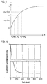
- the results are shown by solid circle marks in Fig. 6. It is seen from Fig. 6 that the loaded Q l increases with a decrease in the thickness of the magnetic garnet films.
- the measured values and the calculated values of unloaded Q u of the magnetic garnet films used in the above experiment were determined.
- the measured values of the unloaded Q u were determined by the following procedures. First, a magnetic garnet film having a thickness of 95 ⁇ m was used as such, and the distance between an input/output electrodes was arranged to be 960 ⁇ m, to prepare a filter which showed an input power/output power ratio of at least 30 dB.
- Fig. 7 shows the results as solid circles.
- ⁇ H is 179.1 A/m when the resonance frequency is 9.55 Hz, and it decreases nearly in proportion to frequency. Further, an offset value is present.
- Fig. 7 shows the results by a solid line. It is seen from Fig. 7 that the measured values and the calculated values of the unloaded Q u are approximately in agreement. It is because ⁇ H gradually increases due to a low magnetic field loss that, in Fig. 7, the measured values deviate from the calculated values in a frequency region of 1.5 GHz or smaller.
- a calculated value of the loaded Q l was determined on the basis of the unloaded Q u .
- 1/Q t refers to a reciprocal number sum of a Q s value based on a conductor loss and a radiation loss of a microstripline formed on a magnetic garnet film and a dielectric loss and a Q 0 value based on other factors.
- the measured value of the unloaded Q u was about 700 at a frequency of 700 MHz, wherefore a circuit prepared by connecting an equivalent parallel resonator of a YIG resonator having the above value and a microstripline in series is simulated with a 50 ⁇ port to determine a loaded Q l .
- the result is that the loaded Q l is 300 to 350 even if it is taken into consideration that the conductor loss varies to a great extent depending upon the thickness and the width of the microstipline.
- the measured value of the loaded Q l is very small, as small as 100 or less, as shown in Fig. 6.
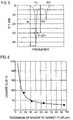
- Fig. 8 shows a relationship of a rectangular magnetic garnet film 1, standing waves generated therein at resonance and an exciting electrode (RF signal feeder line 4). It is to be assumed that an external magnetic field Hex is applied perpendicularly to the film surface of the magnetic garnet film 1. It is generally assumed that, in side surfaces 1c and 1d of the magnetic garnet film 1, i.e., a boundary of the inside of the film and the outside of the film, a DC magnetic field intensity comes to be discrete due to an anti-magnetic field of the magnetic garnet film, so that magnetostatic wave which has propagated through the magnetic garnet film 1 is nearly completely pinned in the side surfaces 1c and 1d to be totally reflected. And, in the case of Fig. 8, it is assumed that standing wave having a basic mode of a distance L between the opposing side surfaces 1c and 1d is generated to cause a resonance.
- a standing wave 28 having a longer wavelength (frequency ⁇ 0 - ⁇ 1 ) and a standing wave 29 having a smaller wave length (frequency ⁇ 0 + ⁇ 2 ) are generated.
- ⁇ L and ⁇ H are respectively a lower-limit frequency and an upper limit frequency of magnetostatic wave which can be excited when an external magnetic field having a predetermined intensity is applied.
- the intensity of an external magnetic field to be applied is constant, it is considered on the basis of Fig. 9 that the resonance frequency of the standing wave having a longer wavelength becomes lower than the frequency ⁇ 0 and that the resonance frequency of the standing wave having a smaller wavelength becomes higher than the frequency ⁇ 0 .
- a 1 mm ⁇ magnetic garnet film i.e., a magnetic garnet film having a length L of 1 mm
- an RF signal feeder line 4 having a structure shown in Fig. 8 was formed thereon, to prepare an exciting electrode.
- ⁇ 0 1 mm
- standing waves having various wavelengths in the range of ⁇ 0 ⁇ about 11 % are present in the magnetic garnet film with corresponding to frequencies in the range of from ⁇ 0 - ⁇ 1 to ⁇ 0 + ⁇ 2 where ⁇ 0 is the central frequency.
- arbitrary values of the saturation magnetization of the magnetic garnet film, the film thickness thereof, the wavelength of the basic standing wave thereof and the intensity of external magnetic field to be applied to the magnetic garnet film were selected from the ranges of 0 to 0.176 Wb/m 2 , 5 to 150 ⁇ m, 250 ⁇ m to 4 mm and 0 to 1.592 x 10 5 A/m, respectively, and combined.
- t 1 + t 2 value obtained by deducting the thickness of the magnetic garnet film from the distance between a pair of the two ground conductors sandwiching the magnetic garnet film
- loaded Q l and unloaded Q u were determined by calculation in each case.
- the unloaded Q u varies depending upon combinations of the above various conditions, while it does not depend upon t 1 + t 2 . Therefore, a increase in the loaded Q l /unloaded Q u with a decrease in t 1 + t 2 in each combination means that the loaded Q l increases with a decrease in t 1 + t 2 in each combination.
- the loaded Q l can be increased regardless of the other conditions.
- it is required to provide a predetermined distance or more between the RF signal feeder line and the ground conductor. Since it is sufficient to provide a distance of at least 5 ⁇ m as the above distance, the present invention employs t 1 ⁇ t R + 5 ⁇ m when the thickness of the RF signal feeder line is t R (see Fig. 1).
- the magnetic garnet film and the ground conductor may be in contact, and therefore, t 2 ⁇ 0 ⁇ m
- the ratio of t 1 and t 2 is not specially limited, and it can be properly determined depending upon a use field of the magnetostatic wave device. For example, when it is used in a region of relatively low frequency, generally, t 1 >t 2 is employed. In the case of t 1 >t 2 , t 1 + t 2 ⁇ 300 ⁇ m is employed, whereby a more preferable result can be obtained.
- the magnetic reluctance of a closed magnetic circuit formed of the void 9b - the magnetic pole piece 7b - the yoke 12a - the magnetic pole piece 7a - the void 9a - the magnetic pole piece 8a - the yoke 12b - the magnetic pole piece 8b in the magnetic field generator shown in Fig. 3A can be decreased by decreasing the distance between the ground conductors, so that the coils 17 can generate an intense magnetic field at small currents or with a smaller winding number of the coils.
- the volume of the coils can be therefore decreased, whereby the magnetic field generator as a whole can be decreased in size.
- the present invention can be also applied to the configuration shown in Fig. 4, i.e., a configuration in which the void 9, the permanent magnet 11 and the coil 17 are arranged in series in the height direction.
- Fig. 4 it is difficult to control the height of the magnetostatic wave device as a whole even if t 1 + t 2 is controlled according to the present invention, i.e., even if the void length of the void 9 is controlled so as to be small, the configuration of Fig. 4 is difficult to decrease in size.
- Example 2 shows the results.
- (t 2 50 ⁇ m) Sample No. t 1 ( ⁇ m) t 1 + t 2 ( ⁇ m) Relative value of loaded Q l /unloaded Q u 201 150 200 135 202 200 250 123 203 250 300 115.5 204 300 350 110 205 350 400 107 206 450 500 103.5 207 (Comparative) 750 800 100
- Tables 1 to 3 shows that the loaded Q l /unloaded Q u is sharply increased by bringing t 1 + t 2 into the predetermined range.
Landscapes
- Control Of Motors That Do Not Use Commutators (AREA)
- Thin Magnetic Films (AREA)
Applications Claiming Priority (3)
| Application Number | Priority Date | Filing Date | Title |
|---|---|---|---|
| JP21408397 | 1997-07-24 | ||
| JP21408397 | 1997-07-24 | ||
| PCT/JP1998/002910 WO1999005751A1 (fr) | 1997-07-24 | 1998-06-29 | Dispositif d'ondes magnetostatiques |
Publications (2)
| Publication Number | Publication Date |
|---|---|
| EP0929114A1 true EP0929114A1 (fr) | 1999-07-14 |
| EP0929114A4 EP0929114A4 (fr) | 2004-06-09 |
Family
ID=16649965
Family Applications (1)
| Application Number | Title | Priority Date | Filing Date |
|---|---|---|---|
| EP98929742A Withdrawn EP0929114A4 (fr) | 1997-07-24 | 1998-06-29 | Dispositif d'ondes magnetostatiques |
Country Status (5)
| Country | Link |
|---|---|
| US (1) | US6114929A (fr) |
| EP (1) | EP0929114A4 (fr) |
| KR (1) | KR100296472B1 (fr) |
| CN (1) | CN1123946C (fr) |
| WO (1) | WO1999005751A1 (fr) |
Families Citing this family (8)
| Publication number | Priority date | Publication date | Assignee | Title |
|---|---|---|---|---|
| JPH11102815A (ja) * | 1997-09-29 | 1999-04-13 | Murata Mfg Co Ltd | 静磁波デバイス |
| CN1159737C (zh) | 1999-04-22 | 2004-07-28 | Tdk株式会社 | 静磁波器件 |
| JP3539322B2 (ja) * | 1999-12-09 | 2004-07-07 | 株式会社村田製作所 | 静磁波素子 |
| US7162302B2 (en) | 2002-03-04 | 2007-01-09 | Nanoset Llc | Magnetically shielded assembly |
| US7091412B2 (en) | 2002-03-04 | 2006-08-15 | Nanoset, Llc | Magnetically shielded assembly |
| CN110165344B (zh) * | 2019-05-28 | 2021-08-27 | 西南应用磁学研究所 | 旋磁滤波器谐振电路结构 |
| CN111787778B (zh) * | 2020-08-04 | 2025-04-08 | 中国电子科技集团公司第九研究所 | 一种yig滤波器抗辐射附加屏蔽结构及带有该附加屏蔽结构的滤波器 |
| CN114914647B (zh) * | 2022-05-17 | 2023-04-28 | 电子科技大学 | 一种基于铁氧体材料的可调谐宽带带阻滤波器 |
Family Cites Families (10)
| Publication number | Priority date | Publication date | Assignee | Title |
|---|---|---|---|---|
| CA1204181A (fr) * | 1982-12-06 | 1986-05-06 | Yoshikazu Murakami | Resonateur ferromagnetique |
| JPS61224702A (ja) * | 1985-03-29 | 1986-10-06 | Sony Corp | 強磁性共鳴装置 |
| US4983936A (en) * | 1986-07-02 | 1991-01-08 | Sony Corporation | Ferromagnetic resonance device |
| US4751480A (en) * | 1986-11-14 | 1988-06-14 | Hewlett-Packard Company | One port magnetostatic wave resonator |
| GB2198006B (en) * | 1986-11-28 | 1991-04-17 | Sony Corp | Thin film ferromagnetic resonance tuned filters |
| US4782312A (en) * | 1987-10-22 | 1988-11-01 | Hewlett-Packard Company | Mode selective magnetostatic wave resonators |
| JP2595660B2 (ja) * | 1988-06-01 | 1997-04-02 | ソニー株式会社 | フェリ磁性共鳴装置 |
| JP2660747B2 (ja) * | 1989-05-18 | 1997-10-08 | 株式会社村田製作所 | 静磁波装置 |
| JPH0685507A (ja) * | 1992-09-03 | 1994-03-25 | Hitachi Metals Ltd | 静磁波マイクロ波装置 |
| US5309127A (en) * | 1992-12-11 | 1994-05-03 | The United States Of America As Represented By The Secretary Of The Army | Planar tunable YIG filter |
-
1998
- 1998-06-29 WO PCT/JP1998/002910 patent/WO1999005751A1/fr not_active Ceased
- 1998-06-29 EP EP98929742A patent/EP0929114A4/fr not_active Withdrawn
- 1998-06-29 CN CN98801046A patent/CN1123946C/zh not_active Expired - Fee Related
-
1999
- 1999-02-10 US US09/247,590 patent/US6114929A/en not_active Expired - Fee Related
- 1999-03-23 KR KR1019997002457A patent/KR100296472B1/ko not_active Expired - Fee Related
Non-Patent Citations (2)
| Title |
|---|
| HANO M ET AL: "FINITE ELEMENT ANALYSIS OF EXCITATION AND TRANSMISSION PROBLEMS OF MAGNETOSTATIC FORWARD VOLUME WAVE" ELECTRONICS & COMMUNICATIONS IN JAPAN, PART II - ELECTRONICS, SCRIPTA TECHNICA. NEW YORK, US, vol. 76, no. 6, 1 June 1993 (1993-06-01), pages 23-33, XP000420496 ISSN: 8756-663X * |
| See also references of WO9905751A1 * |
Also Published As
| Publication number | Publication date |
|---|---|
| US6114929A (en) | 2000-09-05 |
| CN1234914A (zh) | 1999-11-10 |
| WO1999005751A1 (fr) | 1999-02-04 |
| KR100296472B1 (ko) | 2001-08-07 |
| KR20000068615A (ko) | 2000-11-25 |
| EP0929114A4 (fr) | 2004-06-09 |
| CN1123946C (zh) | 2003-10-08 |
Similar Documents
| Publication | Publication Date | Title |
|---|---|---|
| Carter | Magnetically-tunable microwave filters using single-crystal yttrium-iron-garnet resonators | |
| Matthaei | Magnetically tunable band-stop filters | |
| US6114929A (en) | Magnetostatic wave device with specified distances between magnetic garnet film and ground conductors | |
| Lin et al. | Integrated non-reciprocal dual H-and E-field tunable bandpass filter with ultra-wideband isolation | |
| EP0836276A2 (fr) | Dispositif à ondes magnétostatiques | |
| Kagita et al. | Electrically tunable ferrite bandpass filter in X-band with wide tunability | |
| US12132462B2 (en) | Magnetically tunable ferrimagnetic filter | |
| Roschmann | Compact YIG bandpass filter with finite-pole frequencies for applications in microwave integrated circuits (short papers) | |
| Röschmann | YIG filters | |
| US4983936A (en) | Ferromagnetic resonance device | |
| Carter | Side-wall-coupled, strip-transmission-line magnetically tunable filters employing ferrimagnetic YIG resonators | |
| US5053734A (en) | Magnetostatic wave device | |
| JP2004537905A (ja) | 極超短波共振回路ならびにそのような共振回路を使用した同調可能な極超短波フィルタ | |
| JP2522579B2 (ja) | Pll制御を行う静磁波マイクロ波発振装置 | |
| KR960006463B1 (ko) | 강자성 공명 장치 및 필터 장치 | |
| JPH07321514A (ja) | 強磁性磁気共鳴装置 | |
| JPWO1999005751A1 (ja) | 静磁波デバイス | |
| Carter et al. | Unloaded Q of Single Crystal Yttrium-Iron-Garnet Resonator as a Function of Frequency (Correspondence) | |
| US5289143A (en) | Magnetostatic wave device | |
| JP3272967B2 (ja) | 静磁波デバイスおよびこれを用いた電圧制御発振器 | |
| RU2813745C1 (ru) | Управляемый пространственно-частотный фильтр свч сигнала на спиновых волнах | |
| JP2010273000A (ja) | 電子同調バンドパスフィルター | |
| Cismaru et al. | CPW cascaded magnetostatic-wave bandstop resonators | |
| Soohoo | A ferrite cutoff switch | |
| Tsutsumi et al. | On the YIG film waveguides |
Legal Events
| Date | Code | Title | Description |
|---|---|---|---|
| PUAI | Public reference made under article 153(3) epc to a published international application that has entered the european phase |
Free format text: ORIGINAL CODE: 0009012 |
|
| 17P | Request for examination filed |
Effective date: 19990329 |
|
| AK | Designated contracting states |
Kind code of ref document: A1 Designated state(s): DE FR GB SE |
|
| A4 | Supplementary search report drawn up and despatched |
Effective date: 20040423 |
|
| STAA | Information on the status of an ep patent application or granted ep patent |
Free format text: STATUS: THE APPLICATION HAS BEEN WITHDRAWN |
|
| 18W | Application withdrawn |
Effective date: 20040421 |