EP0929168A2 - Systèmem et/ou méthode de détection et d'asservissement de la phase d'échantillonage dans des systèmes de transmission synchrone - Google Patents
Systèmem et/ou méthode de détection et d'asservissement de la phase d'échantillonage dans des systèmes de transmission synchrone Download PDFInfo
- Publication number
- EP0929168A2 EP0929168A2 EP98440298A EP98440298A EP0929168A2 EP 0929168 A2 EP0929168 A2 EP 0929168A2 EP 98440298 A EP98440298 A EP 98440298A EP 98440298 A EP98440298 A EP 98440298A EP 0929168 A2 EP0929168 A2 EP 0929168A2
- Authority
- EP
- European Patent Office
- Prior art keywords
- clock signal
- signal
- signals
- circuit
- phase
- Prior art date
- Legal status (The legal status is an assumption and is not a legal conclusion. Google has not performed a legal analysis and makes no representation as to the accuracy of the status listed.)
- Granted
Links
- 238000005070 sampling Methods 0.000 title claims abstract description 55
- 230000005540 biological transmission Effects 0.000 title claims abstract description 43
- 238000000034 method Methods 0.000 title claims abstract description 24
- 230000001360 synchronised effect Effects 0.000 title claims abstract description 21
- 230000003111 delayed effect Effects 0.000 claims description 59
- 230000001934 delay Effects 0.000 claims description 5
- GUJDUXMBBAOBHN-UHFFFAOYSA-N 6-(dimethylamino)-n-(2h-tetrazol-5-yl)pyrazine-2-carboxamide Chemical compound CN(C)C1=CN=CC(C(=O)NC2=NNN=N2)=N1 GUJDUXMBBAOBHN-UHFFFAOYSA-N 0.000 claims description 4
- 238000001514 detection method Methods 0.000 claims description 4
- 230000006870 function Effects 0.000 claims description 4
- 238000005259 measurement Methods 0.000 claims 2
- 101000685663 Homo sapiens Sodium/nucleoside cotransporter 1 Proteins 0.000 description 7
- 102100023116 Sodium/nucleoside cotransporter 1 Human genes 0.000 description 7
- 238000004891 communication Methods 0.000 description 7
- 101000821827 Homo sapiens Sodium/nucleoside cotransporter 2 Proteins 0.000 description 6
- 102100021541 Sodium/nucleoside cotransporter 2 Human genes 0.000 description 6
- 239000006185 dispersion Substances 0.000 description 6
- 230000000694 effects Effects 0.000 description 6
- 238000010586 diagram Methods 0.000 description 5
- 230000007613 environmental effect Effects 0.000 description 5
- 230000008901 benefit Effects 0.000 description 4
- 238000005516 engineering process Methods 0.000 description 4
- 230000010363 phase shift Effects 0.000 description 4
- 101100421188 Caenorhabditis elegans smp-1 gene Proteins 0.000 description 3
- 230000008859 change Effects 0.000 description 2
- 230000010354 integration Effects 0.000 description 2
- 238000004519 manufacturing process Methods 0.000 description 2
- 238000012545 processing Methods 0.000 description 2
- 230000032683 aging Effects 0.000 description 1
- 230000000295 complement effect Effects 0.000 description 1
- 230000007547 defect Effects 0.000 description 1
- 230000007257 malfunction Effects 0.000 description 1
- 230000004048 modification Effects 0.000 description 1
- 238000012986 modification Methods 0.000 description 1
Images


Classifications
-
- H—ELECTRICITY
- H04—ELECTRIC COMMUNICATION TECHNIQUE
- H04L—TRANSMISSION OF DIGITAL INFORMATION, e.g. TELEGRAPHIC COMMUNICATION
- H04L7/00—Arrangements for synchronising receiver with transmitter
- H04L7/02—Speed or phase control by the received code signals, the signals containing no special synchronisation information
- H04L7/033—Speed or phase control by the received code signals, the signals containing no special synchronisation information using the transitions of the received signal to control the phase of the synchronising-signal-generating means, e.g. using a phase-locked loop
- H04L7/0337—Selecting between two or more discretely delayed clocks or selecting between two or more discretely delayed received code signals
- H04L7/0338—Selecting between two or more discretely delayed clocks or selecting between two or more discretely delayed received code signals the correction of the phase error being performed by a feed forward loop
Definitions
- the present invention relates to a system and/or method for recognizing and tracking the sampling phase of a signal received in a local terminal, in digital synchronous transmission systems.
- Digital communication systems are often faced with the condition of a local oscillator generating the frequency to transmit data to a remote receiving terminal which, by extracting clock information from the data themselves, e.g. through a Phase Locked Circuit, PLL, uses such a frequency both for reading the data received and timing its own operations.
- PLL Phase Locked Circuit
- a general schematics of a communication system as above is shown by way of example, where a main local terminal TL arranged with a local clock OL is provided.
- Said local clock OL provides for timing, i.e. a transmission clock signal CK, to a transmitter circuit TXL contained in the main local terminal TL.
- the latter communicates with a remote terminal TR having a phase locked circuit PLL at its input, which can be synchronized with the clock frequency of the signal from the transmitter TXL according to the local clock OL.
- Said phase locked circuit PLL will then supply the clock signal locked to the local clock frequency OL to both a receiver RXR and a transmitter TXR, both included in the remote terminal TR.
- the receiver RXR is able to decode the transmitted signal according to the local clock frequency OL.
- the transmitter TXR is able to communicate with a receiver RXL located on the main local terminal TL at the same clock frequency.
- the receiver RXL is also provided on its turn with a further phase locked circuit PLL which is able to synchronize it with the signal from the transmitter TXR.
- the receiver RXL receives the signal directly from the local clock OL and is timed by it on the signal from the transmitter TXR.
- clock information in a communication system as described in Fig.1a is not transmitted explicitly, i.e. as a coded information data but is substantially obtained from the data transmitted through a PLL circuit.
- the receiver contained in the local terminal should also be able to carry out a correct sampling of the data transmitted from the remote terminal. Since the clock frequency is the same for both the local terminal and the remote terminal, as previously mentioned, the only problem is to recognize the phase of the signal which has been re-transmitted from the remote terminal and to be able to, possibly, follow its changes.
- a possible solution is to also provide the local terminal receiver with a further PLL circuit for automatic locking to the clock frequency of the signal re-transmitted from the remote terminal.
- PLL circuits will generally introduce a "jitter", i.e. a frequency distortion, resulting in phase shifts.
- jitter also called “wander” is also generated in the clock signal by the small changes of the operating point of the various circuits, due to temperature changes, power supply value and aging.
- Another object of this invention is to provide a system and/or method for recognizing and tracking the sampling phase of a signal received in a local terminal, in digital synchronous transmission systems, which can be easily implemented and integrated in digital circuits.
- the present invention provides a system and/or method for recognizing and tracking the sampling phase of a signal received in a local terminal, in digital synchronous transmission systems, incorporating the features contained in the annexed claims, which form an integral part of this description.
- Fig. 1b a communication system similar to that represented in Fig. 1a is shown, the only difference being in its local terminal TL1 based on a different concept, whereas the remote terminal TR remains the same as represented in Fig. 1a.
- Said local terminal TL1 contains the transmitter TXL, as well as the local clock OL and the receiver RXL.
- a phase alignment or phase tracking circuit DPA is also provided.
- Said phase alignment circuit DPA will receive at its input the transmission clock signal CK of the local clock OL and output a selected clock signal CKSEL to the receiver RXL as its clock signal.
- Said phase alignment circuit DPA also receives the entering data flow DTP from the transmitter TXR.
- the selected clock signal CKSEL is a clock signal following the phase shifts of the entering data flow DTP thus allowing the receiver RXL to make a minimum error about the sampling phase.
- FIG. 2 the diagrams of four isofrequential clock signals are shown, which are required for implementing the system according to this invention.
- a transmission clock signal CK which is the local clock signal OL
- an quadrature clock signal CKQ i.e. having a quarter-period phase difference with respect to the transmission clock signal CK
- a complentary clock signal CKN corresponds to the complentary transmission clock signal CK i.e. with a half-cycle phase difference, and also a complentary clock signal CKQ is provided as well.
- the quadrature clock signal CKQ is obtained by means of digital techniques better explained hereinbelow by way of example in Fig. 3a and particularly with reference to Figs. 5 and 6. It can be also easily obtained through a quarter period delay line.
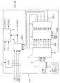
- Fig. 3a the phase alignment circuit DPA according to the invention is represented.
- An input data DTP flow entering through a phase and sampling detector 1; said phase and sampling detector 1 receives at its input the four clock signals CK, CKQ, CKN, CKQN.
- the four clock signals CK, CKQ, CKN, CKQN are obtained through a quadrature signal generator circuit QUAD, which obtains them starting from the transmission clock signal CK of the local clock OL received at its input.
- the four clock signals CK, CKQ, CKN, CKQN are also brought to four alignment circuit DPA terminals to be supplied to other points of said alignment circuit DPA, such as the inputs of the phase and sampling detector 1 and other circuits to be described later.
- the phase and sampling detector 1 outputs a 4-bit (a, b, c, d) phase information F, obtained by the input data flow DTP.
- Said phase information F enters a selection logic 2.
- Said selection logic 2 consists of a finite state machine, whose operation is represented in Fig. 4b, which is timed by the transmission clock signal CK and manages the use of all four clock signals CK, CKQ, CKN, CKQN through a group of enable signals SAB.
- a sampling and phase re-timing circuit 3 receives enable signals SAB and transmits them to a latch block 5, i.e. a transit memory circuit block, wherein four selection signals SSEL of clock signals CK, CKQ, CKN, CKQN are produced.
- Said four selection signals SSEL are sent to a multiplexer circuit 6, which receives at its input the four clock signals CK, CKQ, CKN, CKQN.
- the selected clock signal CKSEL chosen among the four clock signals CK, CKQ, CKN, CKQN is then output from the multiplexer circuit 6.
- a period stretching and sampling circuit 7 which receives at its input the input data flow DTP and a complentary input data flow DTN, which is complementary with respect to the input data flow DTP, and will output a flow of sampled data DTPC and its complentary flow DTNC.
- Said period stretching and sampling circuit 7 is substantially a latch performing the following operation on a bit of the input data flow DTP or of the complentary input data flow DTN: it extends the cycle till a new edge of the selected clock signal CKSEL occurs.
- Circuit operation can be summarized as follows.
- the input data flow DTP reaches the phase and sampling detector input 1, where its unknown phase is compared to each one of the four clock signals CK, CKQ, CKN, CKQN. In this instance, sampling of the input data flow DTP is performed in accordance with the transmission clock signal CK.
- selection logic output 2 consists of enable signals SAB, which will be described better in Fig. 3b, first going through the sampling and phase re-timing circuit 3 which carries out their sampling according to the transmission clock signal CK.
- the purpose of said sampling is to have a full clock signal period for the settling of the combinatory logic of selection logic 2, which is useful specifically in high frequency applications.
- the latch block 5 is used to store the selection status provided by signals SSEL and reach a condition where switching is only permitted between adjacent clock signals. This condition is imposed to let the subsequent multiplexer circuit 6 change the selected clock signal CKSEL without possibly generating any false edges, which could obviously lead to malfunctions. As a matter of fact, if switching occurs between adjacent clock signals and if enable/disable switching of a selected clock signal CKSEL is performed using the raising edge and the lowering edge, respectively, of the clock signal itself, then this could possibly lead to false edges generation.
- the multiplexer circuit 6 outputs the selected clock signal CKSEL, which is then used to sample the input data flow DTP introducing a tolerance in the sampling phase through the period stretching and sampling circuit 7, so as to consider the uncertainty of the phase detecting and sampling circuit 1 in detecting the phase F of the input data flow DTP.
- the flow of sampled data DTPC and the complentary flow of sampled data DTPN are then transmitted to a processing logic not shown here, but obviously available in every communication system as for the type represented in Fig. 1b. Also the selected clock signal CKSEL is supplied to said processing logic.
- the phase detecting and sampling circuit 1 consists of a first group of four flip-flop circuits 11, receiving on their data input the input data flow DTP and at each clock input one of the four clock signals CK, CKQ, CKN, CKQN, so as to perform phase detection. Sampling is performed by a second group of four flip-flop circuits 12 clocked according to the transmission clock signal CK.
- the selection logic 2 outputs eight enable signals SAB, SCK_S, SCK_R, SCKQ_S, SCKQ_R, SCKN_S, SCKN_R, SCKQN_S, SCKQN_R, which are enable and disable signal pairs, respectively.
- Decision rules actuated by the selection logic 2 are represented in Figs. 4a and 4b.
- the sampling and phase re-timing circuit 3 consists of a first group of 8 flip-flops 31, which performs sampling according to the timing of the transmission clock signal CK and a second group of 8 flip-flops 41, which performs the phase retiming according to the relevant clock signals CK, CKQ, CKN, CKQN.
- the enable signals SAB will reach the latch block 5 obtained through the four set/reset flip-flops 51, where four signals SCK_MX, SCKQ_MX, SCKN_MX, SCKQN_MX, i.e. the selection signals SSEL for the multiplexer circuit 6, are enable and disable signals for their outputs.
- the same clock signal CK is used to enable SCK_S for the same enable signal, e.g. SCK
- the complentary clock signal CKN is used, which means using the raising edge for one and the descending edge for the other one.
- Fig. 3b shows implementation of the multiplexer 6 through NAND gates to input select a selected clock signal CKSEL out of the four clock signals CK, CKQ, CKN, CKQN.
- Fig. 3b also shows implementation of the period stretching and sampling circuit 7, consisting of two set/reset flip-flops 71, for the input data flow DTP and complentary input data flow DTN, whose outputs are sampled through further flip-flops 72, which operate according to the selected clock signal CKSEL.
- the sampled data flow DTPC and complentary sampled data flow DTPN are also used to return the period stretching and sampling circuit 7 to its initial conditions through the set/reset flip-flops 71.
- Fig. 4a the decision rules actuated by the selection logic 2 are shown.
- the values that can be assumed by the four clock signals CK, CKQ, CKN, CKQN, are indicated, i.e. corresponding substantially to the phase information of the 4-bit data F, a, b, c, d.
- the selected clock signal CKSEL is indicated accordingly.
- the remaining columns report the enable signals SAB accordingly produced.
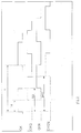
- Fig. 4b shows the operating diagram of the finite state machine contained in the selection logic 2 and corresponding to the decision rules illustrated in the Table of Fig. 4a.
- Inputs due to the phase information of the 4-bit phase data F, a, b, c, d and the hexadecimal coded outputs representing the 8 binary values of the enable signals SAB are also represented.
- 0111/6A corresponds to a phase information F measuring the input clock signal CK (0111)
- the hexadecimal code 6A output corresponds to the binary string 01101010, i.e. the logic values to be sent as set/reset signals to the 8 flip-flops 31.
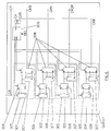
- Fig. 5 shows the quadrature signal generating circuit QUAD able to generate the quadrature clock signal CKQ.
- delay lines may be effectively used to this purpose, however they have the drawback of a rather big size as well as a bad integration with digital technologies, whose application represents one of the objects of this invention.
- the quadrature signal generating circuit QUAD is fully obtained through digital technologies, specifically CMOS technology, which also avoids the drawbacks that hindered the use of digital circuits to generate delays, or dispersion effects in the technological parameters due to the device manufacturing process, or the effect of environmental parameters changes, such as temperature and supply.
- Such drawbacks are mainly overcome by the use of a group of delay cells introducing delay times with a different value to each other and much shorter than the period time of the reference clock signal. A careful selection strategy of said delay times will result in a quadrature clock signal.
- the quadrature signal generating circuit QUAD is in fact divided in two stages: a first stage 100 and a second stage 200.
- the first stage 100 is composed of a first offset delay block 101, which receives at its input the transmission clock signal CK from the local clock OL, and transfers a first offset clock signal CKOFF1 to a first delay block 102.
- the first offset clock signal CKOFF1 is a delayed signal, which is so short with respect to the transmission clock signal CK, that no quadrature clock signal with respect to the transmission clock signal CK can be derived from said first offset clock signal CKOFF1.
- the first delay block 102 is provided with m outputs, at which clock signals CKM_1 ... CKM_M are produced. Clock signals CKM_1 ... CKM_M at m outputs are incrementally phase shifted to each other by a first delay TA. It should be noted that any mention to the first delay TA and second delay TB to be introduced later refers to the nominal values of said delays, without taking into account any changes due to a dispersion of the technological parameters and environmental effects.
- a first multiplexing circuit 103 input receives m clock signals CKM_1 ... CKM_M.
- the clock signal CKM_M with a greater phase shift equal to m times TA is brought to the input of a first logic circuit CL1 consisting of a second offset delay block 104, at whose output a second offset clock signal CKOFF2 is generated.
- the offset time introduced by the second offset delay block 104 must be such to produce a second offset clock signal CKOFF2, which is delayed with respect to the transmission clock signal CK till the raising edge is around the descending edge of the main clock signal CK, but without the raising edge of the second offset clock signal CKOFF2 is prior to the descending edge of the main clock signal CK.
- the second offset clock signal CKOFF2 generated as above will enter a second delay block 106.
- the second delay block 106 operates similarly to the first delay block 102.
- said second delay block 106 is provided with m outputs, where clock signals CKMS_1 ... CKMS2_M are produced.
- Clock signals CKMS_1 ... CKMS_M at m outputs are incrementally phase shifted to each other twice the amount of the first delay TA.
- a second multiplexing circuit 107 receives at its input the m clock signals CKMS_1 ... CKMS_M.
- said clock signals CKMS_1 ... CKMS_M are inputted to a sampler circuit 108, which receives the main clock signal CK at one of its other inputs.
- the sampler circuit 108 samples clock signals CKMS_1 ... CKMS_M through the main clock signal CK.
- a first decision logic 109 receives samples SMP_1 ... SMP_M from the first sampler circuit 108 and selects an approximate quadrature clock signal CKQP among the clock signals CKM_1 ... CKM_M on the first multiplexing circuit 103.
- the selection rule used by the first decision logic 109 is as follows: if samples SMP_1 ... SMP_M from the first to a determined sample SMP_J, whose index j is included between 1 and m, assume the value of logic "1", and the following ones up to the sample SMP_M assume the value of logic '0', the first decision logic 109 will correspondingly select through the first multiplexing circuit 103 the clock signal CKM_J as an approximate quadrature clock signal CKQP.
- the decision logic 109 also controls the second multiplexing circuit 107, which input receives clock signals CKMS_1 ... CKMS_M to select a delayed quadrature clock signal CKQD among said clock signals CKMS_1 ...
- the clock signal CKMS_J is chosen as a quadrature delayed clock signal CKQD, corresponding to the transmission clock signal CK, which is delayed twice j x TA.
- the delayed quadrature clock signal CKQD has its own raising edge around the descending edge of the clock signal CK.
- the approximate quadrature clock signal CKQP is a clock signal approximating the quadrature with respect to the transmission clock signal CK to the extent this is allowed by the value represented by the first delay TA, i.e. in the worst case the quadrature is reached with a maximum deviation equal to the first delay TA.
- the delayed quadrature clock signal CKQD is a clock signal that may be defined in phase quadrature with respect to the transmission clock signal CK to the extent this is allowed by the double of the time value first delay TA, i.e. in the worst case the quadrature is reached with a maximum deviation equal to twice the first delay TA.
- the approximate quadrature clock signal CKQP input enters the second stage 200, and more precisely, a third delay block 201.
- the third delay block 201 has m' outputs, where clock signals CKM'_1 ... CKM'_M' are generated. Clock signals CKM'_1 ... CKM'_M' at m outputs are incrementally phase shifted to each other by a second delay TB.
- a third multiplexing circuit 202 input receives m clock signals CKM'_1 ... CKM'_M' generated to select the quadrature clock signal CKQ.
- the delayed quadrature clock signal CKQD on the contrary, input enters a fourth delay block 203.
- Said fourth delay block 203 also has m' outputs where clock signals CKM'S_1 ... CKM'S_M' are generated.
- Clock signals CKM'S_1 ... CKM'S_M' at m outputs are incrementally phase shifted to each other by a time amount equal to twice the second delay TB so that, as described for the stage 100, a second sampler circuit 205 operating like the first sampler circuit 108 will supply to a second decision logic 206 the information to choose as clock signal samples SMP'_1' ... SMP'_M' between the clock signals CKM'_1 ... CKM'_M', through actuation of the third multiplexer circuit 202, the quadrature clock signal CKQ being the output of the quadrature signal generating circuit QUAD.
- the quadrature clock signal CKQD performs, also for stage 200, the task previously accomplished by the clock signal CK_OFF2 for stage 100, i.e. provides a time reference with the raising edge around the descending edge of the main clock signal CK.
- the clock signal CKM_1 will have a 2 ns delay with respect to the transmission clock signal CK and a clock signal CKM_M delayed by 10 ns with respect to the main clock signal CK.
- quadrature clock signal CKQ should ideally have a delay time of T/4, i.e. about 4,82 ns, so it is easy to determine that the clock signal CKM_3 will be the one to approximate said delay value by defect using the first delay time TA as a step. Said determination is made in fact through the logic circuit CL1.
- the logic circuit CL1 generates clock signals CKMS_1 ... CKMS_M which are phase shifted to each other by the double of the first delay time TA, so that sampling activity of the sampler circuit 108 may cover the whole time period T and detect the position of the descending edge of the main clock signal CK.
- the delayed quadrature clock signal CKQD is obtained through the logic circuit CL1, whose function is to serve as a new reference for the second stage 200.
- the logic circuit CL1 performs the primary function to select the approximate quadrature clock signal CKQP with the precision of the first delay time TA, and further the auxiliary function of providing the second stage 200 with the corresponding delayed quadrature clock signal CKQD, so that the structure does not need to be repeated to correctly drive the second sampler circuit 205.
- the logic circuit CL1 structured as above is necessary since due to a dispersion of technological parameters in digital circuits, the first delay time TA introduced by the various delay cells contained in the first delay block 102 has a different value and may also lead to 100% residual errors between the first delay time TA added e.g. to the signal CKM_1 and the first delay time TA added to the signal CKM_2.
- the circuit CL1 uses substantially the clock signal CKM_M as a reference to generate clock signals CKMS_1 ... CKMS-M being sampled with the known clock signal CK, so as to compensate the dispersion effect of technological parameters on the first delay time TA and correctly drive the first multiplexing circuit 103.
- a main advantage of the signal quadrature generating circuit QUAD described above is its capability to follow period changes and phase deviations of the main clock signal CK, i.e. deviations by 50% from an ideal 'duty period'. Moreover, it will also compensate dispersion effects in technological parameters due to the manufacturing process of the devices in use and varying environmental parameters, such as temperature and supply. Said drawback represented in fact the main restriction to the use of delay cells based on digital circuits against conventional delay lines. Moreover, the circuit described above is fully obtainable under CMOS technology, i.e. it is fully compatible with the phase alignment circuit DPA previously described. It is quite obvious, in the instance of a QUAD circuit, that clock signals CKN and CKQN not shown here are obtained inverting clock signals CK and CKQ according to standard logic signals inversion techniques.
- Fig. 6 shows a quadrature signal generating circuit QUAD1, i.e. a change to the quadrature signal generating circuit QUAD. It consists of four stages 301, 302, 303, 304 featuring an identical structure, i.e. a delay block 305 with n outputs connected with n inputs of a multiplexer circuit 306.
- the output of multiplexer circuit 306 is connected with a delay block 307 having m outputs, the latter being connected with m inputs of a multiplexer circuit 308.
- the delay block 305 assigns the first delay time TA while the delay block 307 the second delay time TB, in the same manner as described with reference to Fig. 5.
- Stages 301, 302, 303 and 304 are connected in cascade, i.e. each stage will receive the output signal, i.e. the multiplexer circuit output 308 of the preceding stage, at its input, i.e. at the input of the delay block 305.
- the only exception being of the first stage 301 that will input receives the main clock signal CK.
- the multiplexer circuit 306 is driven by a counter CNT1 generated by a selection block 309.
- a counter CNT2 driving the multiplexer circuit 308 is generated by said selection block 309.
- the input of selection block 309 is a comparator output CMP, which samples the transmission clock signal CK with a second reference clock signal CKR produced on the fourth stage output 304.
- the selection block 309 has an input SEL, which is able to reset counters CNT1 and CNT2.
- the selection block 309 operates as follows:
- the maximum delay obtainable is on the outputs from stages 301, 302, 303, 304:
- the first delay time TA and the minimum number n have to be chosen as to comply with the following relation in spite of variable technological and environmental conditions: n x TA ⁇ T/4 and the second delay time TB and minimum number m has to be chosen as to comply with the following relation in spite of variable technological and environmental conditions: m x TB ⁇ TA
- the circuit QUAD1 optimizes the position of the four clock signals CK, CKQ, CKN, CKQN as to have a rated distance of a quarter-period from a raising edge to the following one.
- the system and/or method for recognizing and tracking the sampling phase of a signal received in a local terminal, in digital synchronous transmission systems allows for correct sampling of the data transmitted from a remote terminal wherein the clock frequency is synchronized with the local oscillator and to adapt itself with time to the effects caused by either an high or lower frequency "jitter", or other interferences, since it is capable of selecting one of the various phases available to the local terminal, i.e. specifically one of the four clock signals in phase quadrature to each other.
- a further advantage of the system and/or method for recognizing and tracking the sampling phase of a signal received in a local terminal, in digital synchronous transmission systems according to this invention is that there is no need to introduce extremely precise delays for the signals; on the contrary, the correct operation is based on the switching between adjacent clock signals, with said switching being driven by the clock signal edges involved with switching itself.
- phase shifted clock signals which are not shifted by a quarter-period but other phase amounts, such as an eigth-period, to obtain an increased phase detection resolution.
Landscapes
- Engineering & Computer Science (AREA)
- Computer Networks & Wireless Communication (AREA)
- Signal Processing (AREA)
- Synchronisation In Digital Transmission Systems (AREA)
- Emergency Protection Circuit Devices (AREA)
- Radar Systems Or Details Thereof (AREA)
- Stabilization Of Oscillater, Synchronisation, Frequency Synthesizers (AREA)
Applications Claiming Priority (2)
| Application Number | Priority Date | Filing Date | Title |
|---|---|---|---|
| ITTO980007 ITTO980007A1 (it) | 1998-01-07 | 1998-01-07 | Sistema e/o procedimento per il riconoscimento e inseguimento della fase di campionamento in sistemi di trasmissione digitale sincroni. |
| ITTO980007 | 1998-01-07 |
Publications (3)
| Publication Number | Publication Date |
|---|---|
| EP0929168A2 true EP0929168A2 (fr) | 1999-07-14 |
| EP0929168A3 EP0929168A3 (fr) | 2004-02-25 |
| EP0929168B1 EP0929168B1 (fr) | 2007-02-14 |
Family
ID=11416252
Family Applications (1)
| Application Number | Title | Priority Date | Filing Date |
|---|---|---|---|
| EP19980440298 Expired - Lifetime EP0929168B1 (fr) | 1998-01-07 | 1998-12-23 | Système et/ou méthode de détection et d'asservissement de la phase d'échantillonage dans des systèmes de transmission synchrone |
Country Status (3)
| Country | Link |
|---|---|
| EP (1) | EP0929168B1 (fr) |
| DE (1) | DE69837079D1 (fr) |
| IT (1) | ITTO980007A1 (fr) |
Cited By (1)
| Publication number | Priority date | Publication date | Assignee | Title |
|---|---|---|---|---|
| EP1571531A1 (fr) * | 2004-03-05 | 2005-09-07 | Thales | Procédé et dispositif d'échantillonnage de données numériques dans une transmission synchrone, avec maintien de l'intégrité binaire. |
Family Cites Families (3)
| Publication number | Priority date | Publication date | Assignee | Title |
|---|---|---|---|---|
| FR2604043B1 (fr) * | 1986-09-17 | 1993-04-09 | Cit Alcatel | Dispositif de recalage d'un ou plusieurs trains de donnees binaires de debits identiques ou sous-multiples sur un signal de reference d'horloge synchrone |
| US5022057A (en) * | 1988-03-11 | 1991-06-04 | Hitachi, Ltd. | Bit synchronization circuit |
| ATE110505T1 (de) * | 1989-02-23 | 1994-09-15 | Siemens Ag | Verfahren und anordnung zum anpassen eines taktes an ein plesiochrones datensignal und zu dessen abtakten mit dem angepassten takt. |
-
1998
- 1998-01-07 IT ITTO980007 patent/ITTO980007A1/it unknown
- 1998-12-23 EP EP19980440298 patent/EP0929168B1/fr not_active Expired - Lifetime
- 1998-12-23 DE DE69837079T patent/DE69837079D1/de not_active Expired - Lifetime
Cited By (1)
| Publication number | Priority date | Publication date | Assignee | Title |
|---|---|---|---|---|
| EP1571531A1 (fr) * | 2004-03-05 | 2005-09-07 | Thales | Procédé et dispositif d'échantillonnage de données numériques dans une transmission synchrone, avec maintien de l'intégrité binaire. |
Also Published As
| Publication number | Publication date |
|---|---|
| DE69837079D1 (de) | 2007-03-29 |
| EP0929168A3 (fr) | 2004-02-25 |
| EP0929168B1 (fr) | 2007-02-14 |
| ITTO980007A1 (it) | 1999-07-07 |
Similar Documents
| Publication | Publication Date | Title |
|---|---|---|
| US4965884A (en) | Data alignment method and apparatus | |
| US5799048A (en) | Phase detector for clock synchronization and recovery | |
| TWI410791B (zh) | 用以傳送及接收複數個資料位元的裝置與方法 | |
| US3982195A (en) | Method and apparatus for decoding diphase signals | |
| US20080101524A1 (en) | Clock data recovery apparatus | |
| US5689530A (en) | Data recovery circuit with large retime margin | |
| US6970521B2 (en) | Circuit and system for extracting data | |
| US5923190A (en) | Phase detector having a sampling circuit | |
| US7254201B2 (en) | Clock and data recovery circuit and method | |
| US6421404B1 (en) | Phase-difference detector and clock-recovery circuit using the same | |
| US5748123A (en) | Decoding apparatus for Manchester code | |
| US5592519A (en) | Dual frequency clock recovery using common multitap line | |
| EP1113616B1 (fr) | Procédé et circuit de recouvrement de signal d'horloge dans un système de télécommunication | |
| EP0929168B1 (fr) | Système et/ou méthode de détection et d'asservissement de la phase d'échantillonage dans des systèmes de transmission synchrone | |
| US8588355B2 (en) | Timing recovery controller and operation method thereof | |
| KR20070065374A (ko) | 지연 제어 회로 및 방법 | |
| US7023944B2 (en) | Method and circuit for glitch-free changing of clocks having different phases | |
| US4464769A (en) | Method and apparatus for synchronizing a binary data signal | |
| US20040190667A1 (en) | Clock extracting circuit and clock extracting method | |
| US10680606B1 (en) | Timing control device and method for high frequency signal system | |
| EP0973264A1 (fr) | Décodage de flux de cadenses (chip) | |
| US6181757B1 (en) | Retiming method and means | |
| JPH08237104A (ja) | ビット位相検出回路およびビット位相同期回路 | |
| JP3397829B2 (ja) | 位相検出回路 | |
| US7006585B2 (en) | Recovering data encoded in serial communication channels |
Legal Events
| Date | Code | Title | Description |
|---|---|---|---|
| PUAI | Public reference made under article 153(3) epc to a published international application that has entered the european phase |
Free format text: ORIGINAL CODE: 0009012 |
|
| AK | Designated contracting states |
Kind code of ref document: A2 Designated state(s): AT BE CH CY DE DK ES FI FR GB GR IE IT LI LU MC NL PT SE |
|
| AX | Request for extension of the european patent |
Free format text: AL;LT;LV;MK;RO;SI |
|
| RIN1 | Information on inventor provided before grant (corrected) |
Inventor name: CANAVESE, ANGELO Inventor name: CARBONE, STEFANO |
|
| RAP1 | Party data changed (applicant data changed or rights of an application transferred) |
Owner name: STMICROELECTRONICS N.V. |
|
| PUAL | Search report despatched |
Free format text: ORIGINAL CODE: 0009013 |
|
| AK | Designated contracting states |
Kind code of ref document: A3 Designated state(s): AT BE CH CY DE DK ES FI FR GB GR IE IT LI LU MC NL PT SE |
|
| AX | Request for extension of the european patent |
Extension state: AL LT LV MK RO SI |
|
| 17P | Request for examination filed |
Effective date: 20040329 |
|
| 17Q | First examination report despatched |
Effective date: 20040714 |
|
| AKX | Designation fees paid |
Designated state(s): DE ES FR GB |
|
| GRAP | Despatch of communication of intention to grant a patent |
Free format text: ORIGINAL CODE: EPIDOSNIGR1 |
|
| GRAS | Grant fee paid |
Free format text: ORIGINAL CODE: EPIDOSNIGR3 |
|
| GRAA | (expected) grant |
Free format text: ORIGINAL CODE: 0009210 |
|
| AK | Designated contracting states |
Kind code of ref document: B1 Designated state(s): DE ES FR GB |
|
| REG | Reference to a national code |
Ref country code: GB Ref legal event code: FG4D |
|
| REF | Corresponds to: |
Ref document number: 69837079 Country of ref document: DE Date of ref document: 20070329 Kind code of ref document: P |
|
| PG25 | Lapsed in a contracting state [announced via postgrant information from national office to epo] |
Ref country code: ES Free format text: LAPSE BECAUSE OF FAILURE TO SUBMIT A TRANSLATION OF THE DESCRIPTION OR TO PAY THE FEE WITHIN THE PRESCRIBED TIME-LIMIT Effective date: 20070525 |
|
| EN | Fr: translation not filed | ||
| PLBE | No opposition filed within time limit |
Free format text: ORIGINAL CODE: 0009261 |
|
| STAA | Information on the status of an ep patent application or granted ep patent |
Free format text: STATUS: NO OPPOSITION FILED WITHIN TIME LIMIT |
|
| 26N | No opposition filed |
Effective date: 20071115 |
|
| PG25 | Lapsed in a contracting state [announced via postgrant information from national office to epo] |
Ref country code: DE Free format text: LAPSE BECAUSE OF FAILURE TO SUBMIT A TRANSLATION OF THE DESCRIPTION OR TO PAY THE FEE WITHIN THE PRESCRIBED TIME-LIMIT Effective date: 20070515 |
|
| PG25 | Lapsed in a contracting state [announced via postgrant information from national office to epo] |
Ref country code: FR Free format text: LAPSE BECAUSE OF FAILURE TO SUBMIT A TRANSLATION OF THE DESCRIPTION OR TO PAY THE FEE WITHIN THE PRESCRIBED TIME-LIMIT Effective date: 20071005 |
|
| PG25 | Lapsed in a contracting state [announced via postgrant information from national office to epo] |
Ref country code: FR Free format text: LAPSE BECAUSE OF FAILURE TO SUBMIT A TRANSLATION OF THE DESCRIPTION OR TO PAY THE FEE WITHIN THE PRESCRIBED TIME-LIMIT Effective date: 20070214 |
|
| PGFP | Annual fee paid to national office [announced via postgrant information from national office to epo] |
Ref country code: GB Payment date: 20131125 Year of fee payment: 16 |
|
| GBPC | Gb: european patent ceased through non-payment of renewal fee |
Effective date: 20141223 |
|
| PG25 | Lapsed in a contracting state [announced via postgrant information from national office to epo] |
Ref country code: GB Free format text: LAPSE BECAUSE OF NON-PAYMENT OF DUE FEES Effective date: 20141223 |