EP0930168B1 - Tintenstrahldruckkopf und verfahren zur herstellung - Google Patents
Tintenstrahldruckkopf und verfahren zur herstellung Download PDFInfo
- Publication number
- EP0930168B1 EP0930168B1 EP98912773A EP98912773A EP0930168B1 EP 0930168 B1 EP0930168 B1 EP 0930168B1 EP 98912773 A EP98912773 A EP 98912773A EP 98912773 A EP98912773 A EP 98912773A EP 0930168 B1 EP0930168 B1 EP 0930168B1
- Authority
- EP
- European Patent Office
- Prior art keywords
- green sheet
- manufacturing
- head base
- ink jet
- jet printer
- Prior art date
- Legal status (The legal status is an assumption and is not a legal conclusion. Google has not performed a legal analysis and makes no representation as to the accuracy of the status listed.)
- Expired - Lifetime
Links
Images



Classifications
-
- B—PERFORMING OPERATIONS; TRANSPORTING
- B41—PRINTING; LINING MACHINES; TYPEWRITERS; STAMPS
- B41J—TYPEWRITERS; SELECTIVE PRINTING MECHANISMS, i.e. MECHANISMS PRINTING OTHERWISE THAN FROM A FORME; CORRECTION OF TYPOGRAPHICAL ERRORS
- B41J2/00—Typewriters or selective printing mechanisms characterised by the printing or marking process for which they are designed
- B41J2/005—Typewriters or selective printing mechanisms characterised by the printing or marking process for which they are designed characterised by bringing liquid or particles selectively into contact with a printing material
- B41J2/01—Ink jet
- B41J2/135—Nozzles
- B41J2/16—Production of nozzles
- B41J2/1621—Manufacturing processes
- B41J2/1626—Manufacturing processes etching
- B41J2/1629—Manufacturing processes etching wet etching
-
- B—PERFORMING OPERATIONS; TRANSPORTING
- B41—PRINTING; LINING MACHINES; TYPEWRITERS; STAMPS
- B41J—TYPEWRITERS; SELECTIVE PRINTING MECHANISMS, i.e. MECHANISMS PRINTING OTHERWISE THAN FROM A FORME; CORRECTION OF TYPOGRAPHICAL ERRORS
- B41J2/00—Typewriters or selective printing mechanisms characterised by the printing or marking process for which they are designed
- B41J2/005—Typewriters or selective printing mechanisms characterised by the printing or marking process for which they are designed characterised by bringing liquid or particles selectively into contact with a printing material
- B41J2/01—Ink jet
- B41J2/135—Nozzles
- B41J2/14—Structure thereof only for on-demand ink jet heads
- B41J2/14201—Structure of print heads with piezoelectric elements
- B41J2/14233—Structure of print heads with piezoelectric elements of film type, deformed by bending and disposed on a diaphragm
-
- B—PERFORMING OPERATIONS; TRANSPORTING
- B41—PRINTING; LINING MACHINES; TYPEWRITERS; STAMPS
- B41J—TYPEWRITERS; SELECTIVE PRINTING MECHANISMS, i.e. MECHANISMS PRINTING OTHERWISE THAN FROM A FORME; CORRECTION OF TYPOGRAPHICAL ERRORS
- B41J2/00—Typewriters or selective printing mechanisms characterised by the printing or marking process for which they are designed
- B41J2/005—Typewriters or selective printing mechanisms characterised by the printing or marking process for which they are designed characterised by bringing liquid or particles selectively into contact with a printing material
- B41J2/01—Ink jet
- B41J2/135—Nozzles
- B41J2/16—Production of nozzles
- B41J2/1607—Production of print heads with piezoelectric elements
- B41J2/161—Production of print heads with piezoelectric elements of film type, deformed by bending and disposed on a diaphragm
-
- B—PERFORMING OPERATIONS; TRANSPORTING
- B41—PRINTING; LINING MACHINES; TYPEWRITERS; STAMPS
- B41J—TYPEWRITERS; SELECTIVE PRINTING MECHANISMS, i.e. MECHANISMS PRINTING OTHERWISE THAN FROM A FORME; CORRECTION OF TYPOGRAPHICAL ERRORS
- B41J2/00—Typewriters or selective printing mechanisms characterised by the printing or marking process for which they are designed
- B41J2/005—Typewriters or selective printing mechanisms characterised by the printing or marking process for which they are designed characterised by bringing liquid or particles selectively into contact with a printing material
- B41J2/01—Ink jet
- B41J2/135—Nozzles
- B41J2/16—Production of nozzles
- B41J2/1621—Manufacturing processes
- B41J2/1626—Manufacturing processes etching
- B41J2/1628—Manufacturing processes etching dry etching
-
- B—PERFORMING OPERATIONS; TRANSPORTING
- B41—PRINTING; LINING MACHINES; TYPEWRITERS; STAMPS
- B41J—TYPEWRITERS; SELECTIVE PRINTING MECHANISMS, i.e. MECHANISMS PRINTING OTHERWISE THAN FROM A FORME; CORRECTION OF TYPOGRAPHICAL ERRORS
- B41J2/00—Typewriters or selective printing mechanisms characterised by the printing or marking process for which they are designed
- B41J2/005—Typewriters or selective printing mechanisms characterised by the printing or marking process for which they are designed characterised by bringing liquid or particles selectively into contact with a printing material
- B41J2/01—Ink jet
- B41J2/135—Nozzles
- B41J2/16—Production of nozzles
- B41J2/1621—Manufacturing processes
- B41J2/1631—Manufacturing processes photolithography
-
- B—PERFORMING OPERATIONS; TRANSPORTING
- B41—PRINTING; LINING MACHINES; TYPEWRITERS; STAMPS
- B41J—TYPEWRITERS; SELECTIVE PRINTING MECHANISMS, i.e. MECHANISMS PRINTING OTHERWISE THAN FROM A FORME; CORRECTION OF TYPOGRAPHICAL ERRORS
- B41J2/00—Typewriters or selective printing mechanisms characterised by the printing or marking process for which they are designed
- B41J2/005—Typewriters or selective printing mechanisms characterised by the printing or marking process for which they are designed characterised by bringing liquid or particles selectively into contact with a printing material
- B41J2/01—Ink jet
- B41J2/135—Nozzles
- B41J2/16—Production of nozzles
- B41J2/1621—Manufacturing processes
- B41J2/1632—Manufacturing processes machining
-
- B—PERFORMING OPERATIONS; TRANSPORTING
- B41—PRINTING; LINING MACHINES; TYPEWRITERS; STAMPS
- B41J—TYPEWRITERS; SELECTIVE PRINTING MECHANISMS, i.e. MECHANISMS PRINTING OTHERWISE THAN FROM A FORME; CORRECTION OF TYPOGRAPHICAL ERRORS
- B41J2/00—Typewriters or selective printing mechanisms characterised by the printing or marking process for which they are designed
- B41J2/005—Typewriters or selective printing mechanisms characterised by the printing or marking process for which they are designed characterised by bringing liquid or particles selectively into contact with a printing material
- B41J2/01—Ink jet
- B41J2/135—Nozzles
- B41J2/16—Production of nozzles
- B41J2/1621—Manufacturing processes
- B41J2/1632—Manufacturing processes machining
- B41J2/1634—Manufacturing processes machining laser machining
-
- B—PERFORMING OPERATIONS; TRANSPORTING
- B41—PRINTING; LINING MACHINES; TYPEWRITERS; STAMPS
- B41J—TYPEWRITERS; SELECTIVE PRINTING MECHANISMS, i.e. MECHANISMS PRINTING OTHERWISE THAN FROM A FORME; CORRECTION OF TYPOGRAPHICAL ERRORS
- B41J2/00—Typewriters or selective printing mechanisms characterised by the printing or marking process for which they are designed
- B41J2/005—Typewriters or selective printing mechanisms characterised by the printing or marking process for which they are designed characterised by bringing liquid or particles selectively into contact with a printing material
- B41J2/01—Ink jet
- B41J2/135—Nozzles
- B41J2/16—Production of nozzles
- B41J2/1621—Manufacturing processes
- B41J2/164—Manufacturing processes thin film formation
- B41J2/1642—Manufacturing processes thin film formation thin film formation by CVD [chemical vapor deposition]
-
- B—PERFORMING OPERATIONS; TRANSPORTING
- B41—PRINTING; LINING MACHINES; TYPEWRITERS; STAMPS
- B41J—TYPEWRITERS; SELECTIVE PRINTING MECHANISMS, i.e. MECHANISMS PRINTING OTHERWISE THAN FROM A FORME; CORRECTION OF TYPOGRAPHICAL ERRORS
- B41J2/00—Typewriters or selective printing mechanisms characterised by the printing or marking process for which they are designed
- B41J2/005—Typewriters or selective printing mechanisms characterised by the printing or marking process for which they are designed characterised by bringing liquid or particles selectively into contact with a printing material
- B41J2/01—Ink jet
- B41J2/135—Nozzles
- B41J2/16—Production of nozzles
- B41J2/1621—Manufacturing processes
- B41J2/164—Manufacturing processes thin film formation
- B41J2/1643—Manufacturing processes thin film formation thin film formation by plating
-
- B—PERFORMING OPERATIONS; TRANSPORTING
- B41—PRINTING; LINING MACHINES; TYPEWRITERS; STAMPS
- B41J—TYPEWRITERS; SELECTIVE PRINTING MECHANISMS, i.e. MECHANISMS PRINTING OTHERWISE THAN FROM A FORME; CORRECTION OF TYPOGRAPHICAL ERRORS
- B41J2/00—Typewriters or selective printing mechanisms characterised by the printing or marking process for which they are designed
- B41J2/005—Typewriters or selective printing mechanisms characterised by the printing or marking process for which they are designed characterised by bringing liquid or particles selectively into contact with a printing material
- B41J2/01—Ink jet
- B41J2/135—Nozzles
- B41J2/16—Production of nozzles
- B41J2/1621—Manufacturing processes
- B41J2/164—Manufacturing processes thin film formation
- B41J2/1645—Manufacturing processes thin film formation thin film formation by spincoating
-
- B—PERFORMING OPERATIONS; TRANSPORTING
- B41—PRINTING; LINING MACHINES; TYPEWRITERS; STAMPS
- B41J—TYPEWRITERS; SELECTIVE PRINTING MECHANISMS, i.e. MECHANISMS PRINTING OTHERWISE THAN FROM A FORME; CORRECTION OF TYPOGRAPHICAL ERRORS
- B41J2/00—Typewriters or selective printing mechanisms characterised by the printing or marking process for which they are designed
- B41J2/005—Typewriters or selective printing mechanisms characterised by the printing or marking process for which they are designed characterised by bringing liquid or particles selectively into contact with a printing material
- B41J2/01—Ink jet
- B41J2/135—Nozzles
- B41J2/16—Production of nozzles
- B41J2/1621—Manufacturing processes
- B41J2/164—Manufacturing processes thin film formation
- B41J2/1646—Manufacturing processes thin film formation thin film formation by sputtering
-
- B—PERFORMING OPERATIONS; TRANSPORTING
- B41—PRINTING; LINING MACHINES; TYPEWRITERS; STAMPS
- B41J—TYPEWRITERS; SELECTIVE PRINTING MECHANISMS, i.e. MECHANISMS PRINTING OTHERWISE THAN FROM A FORME; CORRECTION OF TYPOGRAPHICAL ERRORS
- B41J2/00—Typewriters or selective printing mechanisms characterised by the printing or marking process for which they are designed
- B41J2/005—Typewriters or selective printing mechanisms characterised by the printing or marking process for which they are designed characterised by bringing liquid or particles selectively into contact with a printing material
- B41J2/01—Ink jet
- B41J2/135—Nozzles
- B41J2/14—Structure thereof only for on-demand ink jet heads
- B41J2002/14387—Front shooter
-
- Y—GENERAL TAGGING OF NEW TECHNOLOGICAL DEVELOPMENTS; GENERAL TAGGING OF CROSS-SECTIONAL TECHNOLOGIES SPANNING OVER SEVERAL SECTIONS OF THE IPC; TECHNICAL SUBJECTS COVERED BY FORMER USPC CROSS-REFERENCE ART COLLECTIONS [XRACs] AND DIGESTS
- Y10—TECHNICAL SUBJECTS COVERED BY FORMER USPC
- Y10T—TECHNICAL SUBJECTS COVERED BY FORMER US CLASSIFICATION
- Y10T29/00—Metal working
- Y10T29/42—Piezoelectric device making
-
- Y—GENERAL TAGGING OF NEW TECHNOLOGICAL DEVELOPMENTS; GENERAL TAGGING OF CROSS-SECTIONAL TECHNOLOGIES SPANNING OVER SEVERAL SECTIONS OF THE IPC; TECHNICAL SUBJECTS COVERED BY FORMER USPC CROSS-REFERENCE ART COLLECTIONS [XRACs] AND DIGESTS
- Y10—TECHNICAL SUBJECTS COVERED BY FORMER USPC
- Y10T—TECHNICAL SUBJECTS COVERED BY FORMER US CLASSIFICATION
- Y10T29/00—Metal working
- Y10T29/49—Method of mechanical manufacture
- Y10T29/49401—Fluid pattern dispersing device making, e.g., ink jet
Definitions
- the present invention relates to an ink jet printer head using a piezo-electric element as a driving source for ejecting an ink and a manufacturing method thereof.
- piezo-electric type ink jet printer head using a piezo-electric element comprising a PZT as an electromechanical conversion element which is a driving source for ejecting a liquid or an ink.
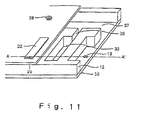
- Fig. 11 illustrates the structure of a typical ink jet printer head of this type: 12 is a head case; 29 is a common electrode (vibrating plate); 32 is a piezo-electric element; 33 is a ink pressure chamber; 35 is a nozzle plate having an ink discharging nozzle port 13; 36 is an ink inlet; 37 is a reservoir; 38 is an ink tank port; and other component elements include a wiring pattern, a signal circuit, an ink tank and the like not shown.
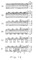
- FIG. 12 schematically illustrates an example of the manufacturing process in the form of a sectional view of Fig. 11 cut along the line A-A'.
- the common electrode 29, a piezo-electric thin film 30 and an upper electrode 31 are sequentially formed on a silicon substrate (wafer) 39.
- a resist layer 15 is formed on the upper electrode 31, exposed and developed into a prescribed pattern through a mask to pattern the resist layer.
- the piezo-electric thin film 30 and the upper electrode 31 are etched with the resist layer 15 as a mask. Then, the resist layer 15 is stripped off, thereby obtaining the piezo-electric element 32.
- a resist layer 15 is formed on the surface opposite to the side on which the piezo-electric element 32 has been formed, exposed and developed into a prescribed pattern through a mask to pattern the resist layer 15.
- the nozzle plate 35 having an ink discharging nozzle port 13 formed at a position corresponding to the ink pressure chamber 33 is connected (adheres) to the thus manufactured head base 12 via an adhering layer or the like as shown in Fig. 12(f). Further, a wiring pattern, a signal circuit, an ink tank and the like are formed to complete an ink jet printer head.
- JP 06023993A and JP 06023993A each discloses a method for fabricating an ink jet head.
- Photosetting resin is cast into a mould and cured by irradiating with ultraviolet light through a masking plate carrying a masking portion. The resin under the masking portion is not cured. The mould is then removed and washed in acetone to remove the uncured resin and thus provide an ink nozzle communicating with an ink passage provided in the cured resin by the shape of the mould.
- ink jet printers are becoming rapidly more popular.
- cost reduction and achievement of a higher resolution of ink jet printers are essential problems to be solved.
- the ink pressure chamber has substantially the same height as the thickness of a silicon wafer.
- the head base and the nozzle plate are connected using an adhesive. It is therefore difficult to prevent undesirable flow of the adhesive into the ink pressure chamber as a result of achievement of a higher resolution.
- the present invention is therefore to solve these problems and has an object to provide a method of manufacturing an ink jet head which permits manufacture thereof through a simple process, enabling a higher resolution at a lower cost.
- the method of operating an ink jet printer head fabricated in accordance with the invention comprises the step of ejecting an ink by pressurizing an ink pressure chamber by deforming, in response to an electrical signal, a piezo-electric element provided on a head base forming the ink pressure chamber.
- a method of manufacturing an ink jet printer head in which ink is ejected by pressurising an ink pressure chamber by means of a piezo-electric element deforming in response to an electric signal, provided on a head base forming said ink pressure chamber; wherein the manufacturing method of said head base comprises a first step of manufacturing a green sheet having a prescribed relief pattern corresponding to a required profile for said head base; a second step of forming said head base by coating and solidifying a material for forming said head base on the surface of said green sheet having said relief pattern; after the second step, a third step of stripping off said head base from said green sheet by irradiating light onto an interface between said green sheet and the head base; and a fourth step of forming a nozzle port for discharging the ink on said head base.
- the invention permits manufacture of an ink jet printer head formed integrally with an ink ejecting nozzle, and gives an ink jet printer head capable of coping with a higher
- the present invention provides a method of forming a head base through copying of a green sheet. Once manufactured, the green sheet can be used repeatedly as long as the durability permits. The process can therefore be omitted in the manufacture of the second and subsequent head bases, thus making it possible to reduce the number of manufacturing steps and hence the cost.
- the nozzle plate is formed integrally, a higher resolution can easily be achieved.
- the first step can be accomplished, for example, as follows:
- the fourth step may be accomplished as follows:
- the present invention discloses an ink jet printer head manufactured by the steps as described above.
- Fig. 1 illustrates a process of manufacturing a head base in an embodiment of the invention.
- the method of manufacturing a head base of the invention comprises a first step of manufacturing a green sheet 10 having a relief pattern in response to the head base to be manufactured as shown in Fig. 1(a); a second step of forming a head base 12 by coating and solidifying a material for forming the head base onto the surface of the green sheet 10 having the relief pattern as shown in Fig. 1(b); a third step of stripping off the head base 12 from the green sheet 10 as shown in Fig. 1(c); and a fourth step of forming an ink discharging nozzle port 13 on the head base 12 as shown in Fig. 1(d).
- Fig. 2 illustrates a process of manufacturing a green sheet in the first embodiment of the first step.
- the first step is more specifically carried out as follows:
- a commercially available positive type resist prepared by blending a diazonaphthoquinone derivative as a photosensitive agent to the cresol novolak-based resin, commonly in use for the manufacture of a semiconductor device is applicable as it is as a material for forming a resist layer 15.
- the term the positive type resist as used here means a resist of which an exposed region can be selectively removed by a developing solution.
- Forming of the resist layer can be accomplished by any of spin coating, dipping, spray coating, roll coating and bar coating.
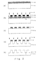
- a mask 16 is arranged on the resist layer 15, and an exposed region 18 is formed by irradiating light 17 onto only a prescribed region of the resist layer 15 through the mask 16.
- a pattern is formed on the mask 16 so that the light 17 transmits only through the region corresponding to the concave portions 11 shown in Fig. 2(e).
- the concave portions 11 are formed in response to the shape and arrangement of the partitions forming the ink pressure chamber, the ink inlet and the reservoir of the ink jet head to be manufactured. After exposure of the resist layer 15, application of the developing treatment under prescribed conditions results in selective removal of the resist only at the exposed region 18 as shown in Fig. 2(c). The green sheet substrate 14 is thus exposed, and the other portions remain as covered with the resist layer 15.
- the green sheet substrate 14 is etched to a prescribed depth with the resist layer 15 as a mask.
- Etching is accomplished either in wet or in dry.
- Wet or dry etching is appropriately selected in response to particular specifications for properties such as material of the green sheet substrate, etching sectional shape and etching rate.
- dry etching is superior: it is possible to etch the concave portions into a desired shape including fabrication into a rectangle or tapering, by changing conditions such as etching gas type, gas flow rate, gas pressure and bias voltage.
- ICP inductive coupling
- ECR electron cyclotron resonance
- high-density plasma etching method such as the helicon wave exciting method are suitable for deeply etching the green sheet substrate 14.
- the resist layer 15 is removed as shown in Fig. 2(e) to obtain the green sheet 10 having a relief pattern in match with the head base.
- the positive type resist has been used when forming the relief pattern on the green sheet substrate.
- a negative type resist may however be used, in which an exposed region is insoluble in the developing solution, and a non-exposed region can be selectively removed by the developing solution.
- a mask having a pattern reverse to that of the mask 16 is employed.
- the resist may directly be patterned in exposure by means of a laser beam or an electron beam without the use of a mask.
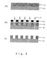
- Figs. 3 and 4 illustrate a process of manufacturing a green sheet in the second embodiment of the first step.
- the first step is carried out as follows:
- the second green sheet 20 takes the role of a support for the resist layer 15 in the process flow.
- the material thereof is not particularly limited so long as a material has process resistance including a mechanical strength and chemicals resistance necessary for the process flow and is satisfactory in wettability and adhesion with the material forming the resist layer 15, including, for example, glass, quartz, a silicon wafer, a resin, a metal and ceramics substrates.
- a glass original plate 20 prepared by polishing flat the surface of the material by the use of a cerium oxide-based abrasive, then washing and drying the same is used here.
- the material and the method described as to the first embodiment mentioned above can be used for the resist layer 15 in the present embodiment, and therefore, description thereof is omitted.
- a mask 21 is arranged on the resist layer 15, and light 17 is irradiated onto only a prescribed region of the resist layer 15 through the mask 21, thereby forming an exposed region 18.
- the mask 21 is patterned so that the light 17 transmits only through the region corresponding to the convex portions of the green sheet 10 to be manufactured, and has a pattern just reverse to that of the mask 16 shown in Fig. 2.
- a conductivity layer 22 is formed on the resist layer 15 and the second green sheet 20 to make the surface conductive.
- the conductivity layer 22 can be formed by any of sputtering, CVD, vapor deposition and electroless plating.
- Ni is electrically deposited by the electroplating method using the resist layer 15 and the second green sheet 20 converted into conductors by the conductivity layer 22 as cathodes and an Ni chip or ball as an anode to form a metal layer 23 as shown in Fig. 4(b).
- a typical composition of the electroplating solution is as follows: Nickel sulfamate 500 g/l Boric acid 30 g/l Nickel chloride 5 g/l Levelling agent 15 mg/l
- the conductivity layer 22 may be removed from the metal layer 23 through a stripping treatment as required.
- the second green sheet 20 can be reused by regeneration and washing as long as the durability thereof permits.
- a negative type resist may used also in the foregoing second embodiment as in the first embodiment, and in this case, a mask having the opposite pattern to in the aforesaid mask 21, i.e., the mask 16 shown in Fig. 2 is used. Or, the resist may be directly exposed in a pattern shape to a laser beam or an electron beam without the use of a mask.
- the material for forming a head base No particular limitation is imposed on the material for forming a head base, but various materials are applicable so long as the requirements for mechanical strength and properties such as corrosion resistance as a head base of an ink jet head are satisfied with a sufficient process durability.
- the material should preferably be hardenable by imparting energy.
- the energy should preferably be light or heat or both light and heat. Use of such energy permits utilization of a general-purpose exposure unit, a baking oven or a hot plate, leading to a lower equipment cost and space saving.
- Applicable substances include, more specifically, acryl resins, epoxy resins, melamine resins, novolak resins, styrene resins, synthetic resins such as polyimide-based ones, and silicon-based polymers such as polysilazane.
- Coating a head base forming material can be accomplished by any of spin coating, dipping, spray coating, roll coating and bar coating.
- the head base forming material contains a solvent component
- a heat treatment should be applied to remove the solvent.
- a thermoplastic substance may be used as a head base forming material.
- Hydrated glass is suitable as such a substance. Hydrated glass contains water within a range of from several to several tens of wt.% and is in a solid state at room temperature. It exhibits plasticity at low temperature (under 100°C, varying with the composition). Dehydration of such a hydrated glass after forming the head base gives a head base excellent in mechanical strength, corrosion resistance and heat resistance.
- stripping step comprises fixing the green sheet 10 having the head base 12 formed thereon, attracting and holding the head base 12, and mechanically stripping it off.
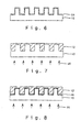
- the concave portions of the relief pattern formed on the green sheet 10 should preferably have a tapered shape having an opening larger than the bottom. This allows to reduce stress such as a frictional force acting between the green sheet 10 and the head base 12 upon stripping, and hence ensure stripping from the green sheet 10.
- a similar effect is available also by forming a stripping layer 24 comprising a material having a low adhesion to the head base 12 on the surface of the green sheet 10 having a relief pattern, as shown in Fig. 6. It suffices to appropriately select a material for the stripping layer 24 in response to the materials for the green sheet 10 and the head base 12.
- Stripping from the green sheet 10 is made satisfactory by irradiating light 25 onto the interface between the green sheet 10 and the head base 12 prior to stripping, as shown in Fig. 7 to reduce or eliminate adhesion between the green sheet and the head base 12. This is to reduce or eliminate various kinds of bonding force between atoms or molecules at the interface of the green sheet 10 and the head base 12, or in practice, to cause ablation or the like, which results in interfacial stripping, under the effect of the irradiated light.
- the irradiated light may in some cases cause release of gases from the head base 12, thereby permitting achievement of a separating effect. More specifically, the components contained in the head base 12 are evaporated and released to contribute to the separation.
- the irradiated light 25 should preferably be an excimer laser.
- the excimer laser is practically applied in an apparatus providing a high energy output in the short wavelength region, and permits treatment in a very short period of time. Ablation is therefore caused only in the proximity of the interface, and hardly exerts a temperature impact onto the green sheet 10 or the head base 12.
- the irradiated light 25 is not limited to the excimer laser, but any of various light beams (radiations) is applicable so long as it can cause interfacial stripping at the interface between the green sheet 10 and the head base 12.
- the green sheet 10 It is necessary for the green sheet 10 to have transmissivity relative to the irradiated light 25.
- the transmissivity should preferably be at least 10%, or more preferably, at least 50%. With a transmissivity lower than this level, attenuation during transmission of the irradiated light through the green sheet, resulting in a larger amount of light required for causing the aforesaid phenomenon such as ablation. Quartz glass, which has a high transmissivity and is excellent also in mechanical strength and heat resistance, is suitable as a material for the original plate.
- a separating layer 26 for causing stripping at the interface with the green sheet 10 under the effect of the irradiated light 25 may be provided between the green sheet 10 and the head base 12.
- Applicable materials for the separating layer 26 include non-crystalline silicon; various oxide ceramics such as silicon oxide, silicate compounds, titanium oxide, titanate compounds, zirconium oxide, zirconate compounds, lanthanum oxide and lanthanate compounds; (strong) dielectric bodies or semiconductors; nitride ceramics such as silicon nitride, aluminum nitride, and titanium nitride; organic polymer materials such as acrylic resins, epoxy resins, polyamide and polyimide; a metal or an alloy of two or more metals selected from the group consisting of Al, Li, Ti, Mn, In, Sn, Y, La, Ce, Nd, Pr, Gd, and Sm. One or more is appropriately selected from among the materials enumerated above in response to the process conditions and the materials for the green sheet and the head base 12.
- a method is appropriately selected in accordance with the composition and the thickness of the separating layer 26. More specifically, applicable methods for forming the separating layer 26 include various gas phase depositing method such as CVD, vapor deposition, sputtering, and ion plating, electroplating, Langmuir Blodgett (LB) method, spin coating, dipping, spray coating, roll coating and bar coating.
- gas phase depositing method such as CVD, vapor deposition, sputtering, and ion plating, electroplating, Langmuir Blodgett (LB) method, spin coating, dipping, spray coating, roll coating and bar coating.
- the thickness of the separating layer 26, varying with the object of stripping or the composition of the separating layer 26, should usually been within a range of from 1 nm to 20 ⁇ m, or more preferably, from 10 nm to 20 ⁇ m, or further more preferably, from 40 nm to 1 ⁇ m.
- a smaller thickness than this level of the separating layer 26 leads to a larger damage to the head base 12, and a larger thickness requires a larger amount of irradiated light for ensuring a good strippability of the separating layer 26.
- the thickness of the separating layer 26 should preferably be uniform as far as possible.
- the residue of the separating layer 26 after stripping is removed through washing.
- the method of forming the ink discharging nozzle port 13 is not limited to a particular one, but applicable methods include, for example, the lithographic method, laser fabrication, FIB fabrication and discharge fabrication.
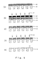
- Fig. 9 illustrates a process of forming an ink discharging nozzle port 13 by the lithographic method. More specifically, the process is carried out as follows:
- a resist layer 15 is formed on the head case 12.
- the material and the method of forming the resist layer 15 may be the same as those described above as to Fig. 2, and are not therefore described here.
- a mask 27 is arranged on the resist layer 15, and light 17 is irradiated only onto a prescribed region of the resist layer 15 through the mask 27, thereby forming an exposed region 18.
- the mask 27 is pattern-formed so that the light 17 transmits only to a region corresponding to the ink discharging nozzle port 13 shown in Fig. 9(e).
- etching is accomplished up to complete penetration through the head base 12 by using the resist layer 15 as a mask.
- Etching may be conducted either in wet or in dry. Etching in wet or in dry is appropriately selected, depending upon the etching sectional shape, etching rate, and surface uniformity for the particular material for the ink jet base 12. In terms of controllability, the dry type is superior, and applicable dry methods include, for example, the parallel flat type reactive ion etching (RIE) method, the inductive coupling (ICP) method, the electron cyclotron resonance (ECR) method, the helicon wave exciting method, the magnetron method, the plasma etching method, and the ion beam etching method.
- RIE parallel flat type reactive ion etching
- ICP inductive coupling
- ECR electron cyclotron resonance
- the ink discharging nozzle port 13 can be etched to a desired shape including a rectangle and a tapered shape, by changing conditions such as the etching gas seed, gas flow rate, gas pressure, bias voltage and the like.
- Lasers applicable for laser fabrication include various gas lasers and solid lasers (semiconductor lasers), and particularly, excimer lasers such as KrF, YAG laser, Ar laser, He-Cd laser and CO 2 laser are suitable. Among others, excimer laser is particularly suitable.
- the excimer laser providing a laser beam of a high energy output in the short wavelength region, permits fabrication in a very short period of time, thus resulting in a high productivity.
- the lithographic method it is possible to form ink discharging nozzle ports 13 at a plurality of positions at a time.
- this method leads to a high equipment cost and a higher materials cost, requiring a larger equipment space.
- the green sheet 10 once manufactured, can be reused repeatedly as long as durability permits.
- the manufacturing steps of the second and subsequent green sheet 10 can therefore be omitted, thus permitting reduction of the number of processes and cost reduction.
- a common electrode 29, a piezo-electric thin film 30 and an upper electrode 31 are sequentially laminated on the third green sheet 28.
- the third green sheet 28 plays a role as a support upon patterning the piezo-electric thin film 30 and the upper electrode 31 into elements, and should preferably have a process durability, particularly satisfactory heat resistance and mechanical strength. After bonding (adhesion) with the head base in a process following patterning of the piezo-electric thin film 30 and the upper electrode 31, stripping is conducted at the interface between the common electrode 29 and the third green sheet 28. Therefore, the third green sheet 28 should preferably not to be very high in adhesion with the common electrode 29.
- the material for the common electrode 29 and the upper electrode 31 is not limited to a particular one so long as the electric conductivity is high.
- Applicable materials include, for example, Pt, Au, Al, Ni and In. It suffices to select appropriately a method of forming the common electrode 29 and the upper electrode 31 in response to the material and the film thickness.
- Applicable methods include, for example, sputtering, vapor deposition, CVD, electroplating and electroless plating.
- PZT lead zirconate-titanate
- a noncrystalline gel thin film is formed by repeating for a prescribed time a cycle comprising coating the common electrode 29 with a PZT-based substance having a composition adjusted to a prescribed one by spin coating, and temporarily baking the same. Further, the coated product is fully baked to obtain a piezo-electric thin film 30 having a perovskite crystal structure.
- sputtering may be used for forming the piezo-electric thin film 30.
- the piezo-electric thin film 30 and the upper electrode 31 are patterned into a piezo-electric element 32 in response to the pattern of the ink pressure chamber 33 of the head base 12 shown in Fig. 10(c).
- Patterning can be carried out, for example, by the use of the lithographic method shown in Fig. 12. Description thereof is therefore omitted here.
- the head base 12 obtained from the process shown in Fig. 1 is bonded, or stuck through an adhesive layer 34, to the third green sheet 28 having the common electrode 29 and the piezo-electric element 32 formed thereon.
- the material for the adhesive layer 34 may be appropriately selected in match with the materials for the head base 12, the common electrode 29 and the piezo-electric element 32.
- the head base 12 the common electrode 29 and the piezo-electric element 32 are integrally stripped off from the green sheet 28.
- a wiring pattern, a signal circuit, an ink tank and the like are incorporated to complete an ink jet printer head.
Landscapes
- Engineering & Computer Science (AREA)
- Manufacturing & Machinery (AREA)
- Physics & Mathematics (AREA)
- Optics & Photonics (AREA)
- Particle Formation And Scattering Control In Inkjet Printers (AREA)
Claims (16)
- Verfahren zur Herstellung eines Tintenstrahldruckkopfes, aus dem Tinte ausgestoßen wird, indem eine Tintendruckkammer (33) mittels eines piezoelektrischen Elements (32) unter Druck gesetzt wird, das sich in Reaktion auf ein elektrisches Signal verformt, und das auf einer Kopfbasis (12) vorgesehen ist, das die Tintendruckkammer (33) bildet; wobei
das Herstellungsverfahren der Kopfbasis (12) umfasst:einen ersten Schritt der Herstellung einer Grünlage (10) mit einem vorgeschriebenen Reliefmuster, das einem benötigten Profil für die Kopfbasis (12) entspricht;einen zweiten Schritt der Ausbildung der Kopfbasis (12) durch Auftragen und Verfestigen eines Materials, um die Kopfbasis (12) auf der Oberfläche der Grünlage (10) mit dem Reliefmuster auszubilden;nach dem zweiten Schritt einen dritten Schritt des Ablösens der Kopfbasis (12) von der Grünlage (10) durch Bestrahlen einer Grenzfläche zwischen der Grünlage und der Kopfbasis mit Licht; undeinen vierten Schritt des Ausbildens einer Düsenöffnung (13) auf der Kopfbasis (12) zum Ausstoßen von Tinte. - Verfahren zur Herstellung eines Tintenstrahldruckkopfes nach Anspruch 1, wobei:der erste Schritt einen Schritt des Ausbildens einer Resistschicht (15) in Reaktion auf ein vorgeschriebenes Muster auf einem Substrat (14) der Grünlage, und das anschließende Herstellen der Grünlage (10) durch Ausbilden des Reliefmusters auf den Substrat (14) der Grünlage durch Ätzen umfasst.
- Verfahren zur Herstellung eines Tintenstrahldruckkopfes nach Anspruch 2, wobei:das Substrat (14) der Grünlage ein Silicium-Wafer (39) ist.
- Verfahren zur Herstellung eines Tintenstrahldruckkopfes nach Anspruch 2, wobei:das Substrat (14) der Grünlage aus einem Quarzglas gefertigt ist.
- Verfahren zur Herstellung eines Tintenstrahldruckkopfes nach Anspruch 1, wobei:der erste Schritt die Schritte umfasst: Ausbilden einer Resistschicht (15) mit einem Reliefmuster entsprechend dem benötigten Profil der Kopfbasis auf einer zweiten Grünlage (20), anschließendes Konvertieren der zweiten Grünlage (20) und der Resistschicht (15) zu Leitern, Ausbilden einer Metallschicht (23) durch elektrisches Abscheiden eines Metalls mittels eines Galvanisierungsverfahrens, und anschließendes Ablösen der Metallschicht (23) von der zweiten Grünlage (20) und der Resistschicht (15), um die Grünlage herzustellen.
- Verfahren zur Herstellung eines Tintenstrahldruckkopfes nach Anspruch 1, wobei:das Material zur Ausbildung der Kopfbasis (12) eine Substanz ist, die durch Beaufschlagen mit Energie aushärtbar ist.
- Verfahren zur Herstellung eines Tintenstrahldruckkopfes nach Anspruch 6, wobei:die Energie Licht oder Wärme, oder sowohl Licht als auch Wärme ist.
- Verfahren zur Herstellung eines Tintenstrahldruckkopfes nach Anspruch 1, wobei:die Kopfbasis (12) aus einer thermoplastischen Substanz gebildet wird.
- Verfahren zur Herstellung eines Tintenstrahldruckkopfes nach Anspruch 8, wobei:die thermoplastische Substanz Hydratglas ist.
- Verfahren zur Herstellung eines Tintenstrahldruckkopfes nach Anspruch 1, wobei:die Vertiefung des Reliefmusters, das auf der Grünlage (10) ausgebildet wird, eine abgeschrägte Form mit einer Öffnung größer als ein Boden aufweist.
- Verfahren zur Herstellung eines Tintenstrahldruckkopfes nach Anspruch 1, wobei:eine Ablösungsschicht (24) eines Materials, das eine geringe Haftung an der Kopfbasis (12) aufweist, auf der Grünlagenoberfläche mit dem Reliefmuster ausgebildet wird.
- Verfahren zur Herstellung eines Tintenstrahldruckkopfes nach Anspruch 1, wobei:die Kopfbasis (12) von der Grünlage (10) abgelöst wird, so dass sich der Bereich der Trennung innerhalb einer Trennschicht (26) und/oder an einer Grenzfläche zur Grünlage (10) befindet, indem die Trennschicht (26) zwischen der Grünlage (10) und der Kopfbasis (12) vorgesehen wird, und indem die Grenzfläche zwischen der Grünlage (10) und der Trennschicht (26) mit Licht bestrahlt wird.
- Verfahren zur Herstellung eines Tintenstrahldruckkopfes nach Anspruch 1, wobei:der vierte Schritt das Ausbilden der Tintenausstoßdüsenöffnung mittels eines Lithographieverfahrens umfasst.
- Verfahren zur Herstellung eines Tintenstrahldruckkopfes nach Anspruch 1, wobei:der vierte Schritt das Ausbilden der Tintenausstoßdüsenöffnung (13) mittels eines Laserstrahls umfasst.
- Verfahren zur Herstellung eines Tintenstrahldruckkopfes nach Anspruch 1, wobei:der vierte Schritt das Ausbilden der Tintenausstoßdüsenöffnung (13) mittels eines konvergierenden lonenstrahls umfasst.
- Verfahren zur Herstellung eines Tintenstrahldruckkopfes nach Anspruch 1, wobei:der vierte Schritt das Ausbilden der Tintenausstoßdüsenöffnung (13) mittels Entladungsfertigung umfasst.
Applications Claiming Priority (3)
| Application Number | Priority Date | Filing Date | Title |
|---|---|---|---|
| JP9778097 | 1997-04-15 | ||
| JP09778097A JP3480235B2 (ja) | 1997-04-15 | 1997-04-15 | インクジェットプリンタヘッドおよびその製造方法 |
| PCT/JP1998/001678 WO1998046431A1 (en) | 1997-04-15 | 1998-04-10 | Ink jet printer head and method for manufacturing the same |
Publications (3)
| Publication Number | Publication Date |
|---|---|
| EP0930168A1 EP0930168A1 (de) | 1999-07-21 |
| EP0930168A4 EP0930168A4 (de) | 2000-07-05 |
| EP0930168B1 true EP0930168B1 (de) | 2004-06-23 |
Family
ID=14201350
Family Applications (1)
| Application Number | Title | Priority Date | Filing Date |
|---|---|---|---|
| EP98912773A Expired - Lifetime EP0930168B1 (de) | 1997-04-15 | 1998-04-10 | Tintenstrahldruckkopf und verfahren zur herstellung |
Country Status (7)
| Country | Link |
|---|---|
| US (1) | US20020184761A1 (de) |
| EP (1) | EP0930168B1 (de) |
| JP (1) | JP3480235B2 (de) |
| CN (1) | CN1159157C (de) |
| DE (1) | DE69824695T2 (de) |
| TW (1) | TW420638B (de) |
| WO (1) | WO1998046431A1 (de) |
Families Citing this family (14)
| Publication number | Priority date | Publication date | Assignee | Title |
|---|---|---|---|---|
| TW506908B (en) * | 2001-09-06 | 2002-10-21 | Nanodynamics Inc | Piezoelectric ink jet print head and the manufacturing process thereof |
| US6886922B2 (en) | 2002-06-27 | 2005-05-03 | Matsushita Electric Industrial Co., Ltd. | Liquid discharge head and manufacturing method thereof |
| US7754999B2 (en) * | 2003-05-13 | 2010-07-13 | Hewlett-Packard Development Company, L.P. | Laser micromachining and methods of same |
| JP2004351879A (ja) * | 2003-05-30 | 2004-12-16 | Kyocera Corp | 圧電インクジェットヘッド |
| US7065874B2 (en) * | 2003-07-18 | 2006-06-27 | Canon Kabushiki Kaisha | Method for making liquid ejection head |
| JP4593309B2 (ja) | 2005-01-21 | 2010-12-08 | 東京応化工業株式会社 | 精密微細空間の天板部形成方法 |
| JP4595669B2 (ja) * | 2005-05-19 | 2010-12-08 | 富士ゼロックス株式会社 | 液滴吐出ヘッドの製造方法 |
| US20090199392A1 (en) * | 2008-02-11 | 2009-08-13 | General Electric Company | Ultrasound transducer probes and system and method of manufacture |
| JP5597327B2 (ja) * | 2010-06-29 | 2014-10-01 | 学校法人東京理科大学 | ダイヤモンド被覆工具およびその製造方法 |
| US10427407B2 (en) * | 2014-03-31 | 2019-10-01 | Hewlett-Packard Development Company, L.P. | Printer circuit board fluid ejection apparatus |
| CN107893245A (zh) * | 2017-11-10 | 2018-04-10 | 江苏新广联科技股份有限公司 | 用于生长金属镍盘的化学电铸溶液及其制备 |
| CN110588177B (zh) * | 2019-09-30 | 2021-01-15 | 西安交通大学 | 一种梁膜式压电阵列打印头的转印制造方法 |
| CN111806093A (zh) * | 2020-06-28 | 2020-10-23 | 中国科学院苏州纳米技术与纳米仿生研究所 | 薄型喷墨打印头及其制作方法、设备 |
| CN112918110B (zh) * | 2021-01-20 | 2022-02-22 | 珠海艾派克微电子有限公司 | 一种喷墨打印头 |
Family Cites Families (9)
| Publication number | Priority date | Publication date | Assignee | Title |
|---|---|---|---|---|
| JPS55118877A (en) * | 1979-03-07 | 1980-09-12 | Canon Inc | Method of manufacturing grooved plate for use in multinozzle recording head |
| JPH0445950A (ja) * | 1990-06-13 | 1992-02-14 | Seiko Epson Corp | インクジェットプリンタヘッド用ノズル板 |
| JP2940121B2 (ja) * | 1990-09-25 | 1999-08-25 | セイコーエプソン株式会社 | インクジェット記録ヘッド用基板の製造方法 |
| ATE200251T1 (de) * | 1991-10-22 | 2001-04-15 | Canon Kk | Verfahren zum herstellen eines tintenstrahlaufzeichnungskopfes |
| JP3133488B2 (ja) * | 1992-07-07 | 2001-02-05 | 富士通株式会社 | インクジェットヘッドの製造方法 |
| JP3105651B2 (ja) * | 1992-07-09 | 2000-11-06 | 富士通株式会社 | インクジェットヘッドの製造方法 |
| EP0585854B1 (de) * | 1992-08-31 | 1998-11-11 | Canon Kabushiki Kaisha | Tintenstrahlkopfherstellungsverfahren mittels Bearbeitung durch Ionen und Tintenstrahlkopf |
| JPH08174845A (ja) * | 1994-12-26 | 1996-07-09 | Canon Inc | 液流路形成用樹脂材料、これを用いた液体噴射記録ヘッド、及びその製造方法 |
| JP3521708B2 (ja) * | 1997-09-30 | 2004-04-19 | セイコーエプソン株式会社 | インクジェット式記録ヘッドおよびその製造方法 |
-
1997
- 1997-04-15 JP JP09778097A patent/JP3480235B2/ja not_active Expired - Fee Related
-
1998
- 1998-04-10 TW TW087105477A patent/TW420638B/zh not_active IP Right Cessation
- 1998-04-10 DE DE69824695T patent/DE69824695T2/de not_active Expired - Lifetime
- 1998-04-10 EP EP98912773A patent/EP0930168B1/de not_active Expired - Lifetime
- 1998-04-10 WO PCT/JP1998/001678 patent/WO1998046431A1/ja not_active Ceased
- 1998-04-10 US US09/202,267 patent/US20020184761A1/en not_active Abandoned
- 1998-04-10 CN CNB988004887A patent/CN1159157C/zh not_active Expired - Fee Related
Also Published As
| Publication number | Publication date |
|---|---|
| DE69824695D1 (de) | 2004-07-29 |
| WO1998046431A1 (en) | 1998-10-22 |
| TW420638B (en) | 2001-02-01 |
| CN1159157C (zh) | 2004-07-28 |
| CN1222885A (zh) | 1999-07-14 |
| DE69824695T2 (de) | 2005-06-30 |
| JP3480235B2 (ja) | 2003-12-15 |
| JPH10286955A (ja) | 1998-10-27 |
| EP0930168A4 (de) | 2000-07-05 |
| EP0930168A1 (de) | 1999-07-21 |
| US20020184761A1 (en) | 2002-12-12 |
Similar Documents
| Publication | Publication Date | Title |
|---|---|---|
| US5006202A (en) | Fabricating method for silicon devices using a two step silicon etching process | |
| US5201987A (en) | Fabricating method for silicon structures | |
| US4412224A (en) | Method of forming an ink-jet head | |
| EP0930168A1 (de) | Tintenstrahldruckkopf und verfahren zur herstellung | |
| EP0949078B1 (de) | Tintenstrahlaufzeichnungskopf und verfahren zu dessen herstellung | |
| US20090322829A1 (en) | Method of forming piezoelectric actuator of inkjet head | |
| KR20030037772A (ko) | 일체형 잉크젯 프린트헤드의 제조 방법 | |
| US20060256162A1 (en) | Liquid jet head and method for producing the same | |
| JPH1086391A (ja) | 基板の表面に粘着層を付着させるための方法 | |
| KR100731310B1 (ko) | 잉크젯 헤드 제조 방법 | |
| JP2000079686A (ja) | 圧電体薄膜素子、圧電体薄膜素子を製造するための原盤、インクジェット式記録ヘッド及びこれらの製造方法 | |
| KR100529307B1 (ko) | 모노리틱 잉크제트 프린트 헤드 및 이의 제조 방법 | |
| CN103072378B (zh) | 一种液体喷头及其制造方法 | |
| US6846068B2 (en) | Monolithic ink-jet printhead and method for manufacturing the same | |
| KR100289606B1 (ko) | 잉크젯 프린트헤드용 챔버판의 패터닝방법과 그에 의해 제조되는 액츄에이터 | |
| EP1361065A1 (de) | Verfahren zur herstellung eines druckkopfs und verfahren zur herstellung eines elektrostatischen stellglieds | |
| KR100467886B1 (ko) | 잉크젯프린터헤드및그제조방법 | |
| CN104015485B (zh) | 液体喷头制造方法、液体喷头和打印装置 | |
| JP7593012B2 (ja) | 圧電アクチュエーター付ウエハ、圧電アクチュエーター付ウエハの製造方法、圧電アクチュエーターの製造方法及びインクジェットヘッドの製造方法 | |
| KR20030083616A (ko) | 액체 사출 장치, 프린터 헤드, 및 액체 사출 장치 제조 방법 | |
| JPH04338550A (ja) | オリフィスプレートの製造方法 | |
| EP0520760A1 (de) | Verfahren zur Herstellung von Düsenplatten | |
| CN101062498A (zh) | 独石流体喷射装置及其制造方法 | |
| JP2005028834A (ja) | 液体吐出ヘッド及びその製造方法 | |
| JPH05286141A (ja) | オリフィスプレートの製造方法 |
Legal Events
| Date | Code | Title | Description |
|---|---|---|---|
| PUAI | Public reference made under article 153(3) epc to a published international application that has entered the european phase |
Free format text: ORIGINAL CODE: 0009012 |
|
| 17P | Request for examination filed |
Effective date: 19990315 |
|
| AK | Designated contracting states |
Kind code of ref document: A1 Designated state(s): DE FR GB IT NL |
|
| A4 | Supplementary search report drawn up and despatched |
Effective date: 20000519 |
|
| AK | Designated contracting states |
Kind code of ref document: A4 Designated state(s): DE FR GB IT NL |
|
| 17Q | First examination report despatched |
Effective date: 20021021 |
|
| GRAP | Despatch of communication of intention to grant a patent |
Free format text: ORIGINAL CODE: EPIDOSNIGR1 |
|
| GRAS | Grant fee paid |
Free format text: ORIGINAL CODE: EPIDOSNIGR3 |
|
| GRAA | (expected) grant |
Free format text: ORIGINAL CODE: 0009210 |
|
| AK | Designated contracting states |
Kind code of ref document: B1 Designated state(s): DE FR GB IT NL |
|
| REG | Reference to a national code |
Ref country code: GB Ref legal event code: FG4D |
|
| REF | Corresponds to: |
Ref document number: 69824695 Country of ref document: DE Date of ref document: 20040729 Kind code of ref document: P |
|
| ET | Fr: translation filed | ||
| PLBE | No opposition filed within time limit |
Free format text: ORIGINAL CODE: 0009261 |
|
| STAA | Information on the status of an ep patent application or granted ep patent |
Free format text: STATUS: NO OPPOSITION FILED WITHIN TIME LIMIT |
|
| 26N | No opposition filed |
Effective date: 20050324 |
|
| PGFP | Annual fee paid to national office [announced via postgrant information from national office to epo] |
Ref country code: FR Payment date: 20110426 Year of fee payment: 14 Ref country code: DE Payment date: 20110406 Year of fee payment: 14 |
|
| PGFP | Annual fee paid to national office [announced via postgrant information from national office to epo] |
Ref country code: NL Payment date: 20110426 Year of fee payment: 14 Ref country code: GB Payment date: 20110406 Year of fee payment: 14 |
|
| PGFP | Annual fee paid to national office [announced via postgrant information from national office to epo] |
Ref country code: IT Payment date: 20110420 Year of fee payment: 14 |
|
| REG | Reference to a national code |
Ref country code: NL Ref legal event code: V1 Effective date: 20121101 |
|
| GBPC | Gb: european patent ceased through non-payment of renewal fee |
Effective date: 20120410 |
|
| REG | Reference to a national code |
Ref country code: FR Ref legal event code: ST Effective date: 20121228 |
|
| PG25 | Lapsed in a contracting state [announced via postgrant information from national office to epo] |
Ref country code: GB Free format text: LAPSE BECAUSE OF NON-PAYMENT OF DUE FEES Effective date: 20120410 |
|
| PG25 | Lapsed in a contracting state [announced via postgrant information from national office to epo] |
Ref country code: IT Free format text: LAPSE BECAUSE OF NON-PAYMENT OF DUE FEES Effective date: 20120410 Ref country code: FR Free format text: LAPSE BECAUSE OF NON-PAYMENT OF DUE FEES Effective date: 20120430 |
|
| REG | Reference to a national code |
Ref country code: DE Ref legal event code: R119 Ref document number: 69824695 Country of ref document: DE Effective date: 20121101 |
|
| PG25 | Lapsed in a contracting state [announced via postgrant information from national office to epo] |
Ref country code: NL Free format text: LAPSE BECAUSE OF NON-PAYMENT OF DUE FEES Effective date: 20121101 |
|
| PG25 | Lapsed in a contracting state [announced via postgrant information from national office to epo] |
Ref country code: DE Free format text: LAPSE BECAUSE OF NON-PAYMENT OF DUE FEES Effective date: 20121101 |