EP0930570A2 - Verbindungsprüfung unter Verwendung von Leiterplatten-Topologiedaten - Google Patents
Verbindungsprüfung unter Verwendung von Leiterplatten-Topologiedaten Download PDFInfo
- Publication number
- EP0930570A2 EP0930570A2 EP99106691A EP99106691A EP0930570A2 EP 0930570 A2 EP0930570 A2 EP 0930570A2 EP 99106691 A EP99106691 A EP 99106691A EP 99106691 A EP99106691 A EP 99106691A EP 0930570 A2 EP0930570 A2 EP 0930570A2
- Authority
- EP
- European Patent Office
- Prior art keywords
- test
- nets
- net
- circuit
- short
- Prior art date
- Legal status (The legal status is an assumption and is not a legal conclusion. Google has not performed a legal analysis and makes no representation as to the accuracy of the status listed.)
- Granted
Links
Images


Classifications
-
- G—PHYSICS
- G01—MEASURING; TESTING
- G01R—MEASURING ELECTRIC VARIABLES; MEASURING MAGNETIC VARIABLES
- G01R31/00—Arrangements for testing electric properties; Arrangements for locating electric faults; Arrangements for electrical testing characterised by what is being tested not provided for elsewhere
- G01R31/28—Testing of electronic circuits, e.g. by signal tracer
- G01R31/317—Testing of digital circuits
- G01R31/3181—Functional testing
- G01R31/3185—Reconfiguring for testing, e.g. LSSD, partitioning
- G01R31/318533—Reconfiguring for testing, e.g. LSSD, partitioning using scanning techniques, e.g. LSSD, Boundary Scan, JTAG
- G01R31/318558—Addressing or selecting of subparts of the device under test
- G01R31/318561—Identification of the subpart
-
- G—PHYSICS
- G01—MEASURING; TESTING
- G01R—MEASURING ELECTRIC VARIABLES; MEASURING MAGNETIC VARIABLES
- G01R31/00—Arrangements for testing electric properties; Arrangements for locating electric faults; Arrangements for electrical testing characterised by what is being tested not provided for elsewhere
- G01R31/28—Testing of electronic circuits, e.g. by signal tracer
- G01R31/317—Testing of digital circuits
- G01R31/3181—Functional testing
- G01R31/3183—Generation of test inputs, e.g. test vectors, patterns or sequences
- G01R31/318307—Generation of test inputs, e.g. test vectors, patterns or sequences computer-aided, e.g. automatic test program generator [ATPG], program translations, test program debugging
-
- G—PHYSICS
- G01—MEASURING; TESTING
- G01R—MEASURING ELECTRIC VARIABLES; MEASURING MAGNETIC VARIABLES
- G01R31/00—Arrangements for testing electric properties; Arrangements for locating electric faults; Arrangements for electrical testing characterised by what is being tested not provided for elsewhere
- G01R31/28—Testing of electronic circuits, e.g. by signal tracer
- G01R31/317—Testing of digital circuits
- G01R31/3181—Functional testing
- G01R31/3185—Reconfiguring for testing, e.g. LSSD, partitioning
- G01R31/318533—Reconfiguring for testing, e.g. LSSD, partitioning using scanning techniques, e.g. LSSD, Boundary Scan, JTAG
- G01R31/318536—Scan chain arrangements, e.g. connections, test bus, analog signals
- G01R31/318538—Topological or mechanical aspects
-
- G—PHYSICS
- G01—MEASURING; TESTING
- G01R—MEASURING ELECTRIC VARIABLES; MEASURING MAGNETIC VARIABLES
- G01R31/00—Arrangements for testing electric properties; Arrangements for locating electric faults; Arrangements for electrical testing characterised by what is being tested not provided for elsewhere
- G01R31/28—Testing of electronic circuits, e.g. by signal tracer
- G01R31/317—Testing of digital circuits
- G01R31/3181—Functional testing
- G01R31/3185—Reconfiguring for testing, e.g. LSSD, partitioning
- G01R31/318533—Reconfiguring for testing, e.g. LSSD, partitioning using scanning techniques, e.g. LSSD, Boundary Scan, JTAG
- G01R31/318544—Scanning methods, algorithms and patterns
- G01R31/31855—Interconnection testing, e.g. crosstalk, shortcircuits
-
- G—PHYSICS
- G01—MEASURING; TESTING
- G01R—MEASURING ELECTRIC VARIABLES; MEASURING MAGNETIC VARIABLES
- G01R31/00—Arrangements for testing electric properties; Arrangements for locating electric faults; Arrangements for electrical testing characterised by what is being tested not provided for elsewhere
- G01R31/28—Testing of electronic circuits, e.g. by signal tracer
- G01R31/317—Testing of digital circuits
- G01R31/3181—Functional testing
- G01R31/3185—Reconfiguring for testing, e.g. LSSD, partitioning
- G01R31/318533—Reconfiguring for testing, e.g. LSSD, partitioning using scanning techniques, e.g. LSSD, Boundary Scan, JTAG
- G01R31/318566—Comparators; Diagnosing the device under test
-
- G—PHYSICS
- G06—COMPUTING OR CALCULATING; COUNTING
- G06F—ELECTRIC DIGITAL DATA PROCESSING
- G06F11/00—Error detection; Error correction; Monitoring
- G06F11/22—Detection or location of defective computer hardware by testing during standby operation or during idle time, e.g. start-up testing
- G06F11/2273—Test methods
Definitions
- In-circuit component test is a type of functional test wherein the performance of each digital integrated circuit (IC) is tested as a functional unit. That is, each component (e.g., digital IC) on the board is tested as if it were electrically isolated from the surrounding circuit.
- the tester e.g., ATE
- the tester must apply input signals directly to the inputs of a DUT (device under test) and must access the outputs of the DUT to observe the output response.
- An ATE system such as the HP3070, uses a "bed-of-nails" (i.e., probes which directly make contact with device I/O (input/output) pins from pads on the surface of the board) fixture to access the required nodes on a board.
- a "bed-of-nails” i.e., probes which directly make contact with device I/O (input/output) pins from pads on the surface of the board
- I/O input/output
- the nodal access required by in-circuit test is often hampered by increasing circuit complexity (e.g., miniaturized components, multi-chip modules, ASIC's, etcetera) and increasing use of such technologies as surface mount and silicon-on-silicon.
- test pattern which has brevity as its primary concern is called a brief test pattern. Brief test patterns tend to provide limited diagnostics. A test pattern which is primarily concerned with diagnostic capabilities is called a high diagnostic test pattern. High diagnostic test patterns tend to be lengthy.
- the counting test is an alternative to the walking bit pattern.
- the counting pattern assigns a unique ID number to each net.
- the net ID numbers are increased in binary counting fashion such that a logarithmic compression in the number of test vectors results.
- the total test length would then be proportional (i.e., this estimation does not account for place holder bits) to 5000 nets times 31 bits or 155,000 test clock cycles. This is a substantial savings in test resources as compared with the minimum 25 million test clock cycles required by the conventional walking bit pattern. It is a greater number of test clock cycles than the minimum 65,000 required for the counting pattern, but with better diagnostics.
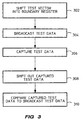
- test vectors have been generated by the method of the invention, then these vectors can be applied to a circuit under test according to the conventional method. That method is described above with reference to Figure 3.
- Figure 12 is a high-level flow chart illustrating the diagnostic method of the invention. In the preferred embodiment, this diagnostic method is performed only if a fault is indicated by the test signature as discussed above.
- the test data (captured test vectors) is analyzed to determine which nets have produced (i.e., captured) identical net signatures.
- Each net signature is made up of the captured bits which were received at a receiving register cell of the net as a result of transmitting a unique net ID number.
- a successful net signature will be identical to the unique net ID number.
- a failure net signature will not match the transmitted net ID number.
- a list 1324 of probable locations of short-circuits is generated at step 1322.
- the list of probable short-circuit locations includes the radially adjacent I/O pins of the PSN's. If, at step 1326, all PSN's in the selected group have been examined, then the method proceeds to step 1328. If, at step 1326, all PSN's in the selected group have not been examined, then the method returns to step 1310 where steps 1310-1326 are repeated for each PSN in the group.
- An unpowered short-circuit test is a type of interconnect test performed before application of power to the components on the circuit board. Each net which can be accessed by a test probe of the ATE is tested to assure that it remains electrically isolated from adjacent nets. It is an object of this test to locate short-circuits between any nets to which the tester has access. Because power is not applied to the circuit board during execution of this test, the potential for damaging a component is substantially reduced. Thus, it is desirable to test as many nets as possible in this manner.
- the unpowered short-circuit test has been performed by contacting each of the n nets on the circuit board with a test probe. A voltage is then applied to a selected net while all other nets are grounded. The applied voltage is selected to have a magnitude (e.g., 0.1 Volts) insufficient to turn on the semiconductor junctions of the components on the circuit board. The current flowing from the probe corresponding to the selected net is monitored to determine whether a short-circuit condition exists between the nets being tested. If the current does not exceed the threshold value, then no short-circuit is indicated for the selected net, and the selected net is eliminated from the set of n nets being tested. Tile test then repeats for a next selected net out of the n-1 remaining nets. The test continues until all tester accessible nets have been tested in this manner.
- a magnitude e.g., 0.1 Volts
Landscapes
- Engineering & Computer Science (AREA)
- General Engineering & Computer Science (AREA)
- Physics & Mathematics (AREA)
- General Physics & Mathematics (AREA)
- Computer Hardware Design (AREA)
- Theoretical Computer Science (AREA)
- Quality & Reliability (AREA)
- Tests Of Electronic Circuits (AREA)
- Testing Of Short-Circuits, Discontinuities, Leakage, Or Incorrect Line Connections (AREA)
Applications Claiming Priority (3)
| Application Number | Priority Date | Filing Date | Title |
|---|---|---|---|
| US08/208,245 US5513188A (en) | 1991-09-10 | 1994-03-09 | Enhanced interconnect testing through utilization of board topology data |
| US208245 | 1994-03-09 | ||
| EP95102281A EP0671689A3 (de) | 1994-03-09 | 1995-02-17 | Verbindungsprüfung unter Verwendung von Leiterplatten-Topologiedaten. |
Related Parent Applications (1)
| Application Number | Title | Priority Date | Filing Date |
|---|---|---|---|
| EP95102281A Division EP0671689A3 (de) | 1994-03-09 | 1995-02-17 | Verbindungsprüfung unter Verwendung von Leiterplatten-Topologiedaten. |
Publications (3)
| Publication Number | Publication Date |
|---|---|
| EP0930570A2 true EP0930570A2 (de) | 1999-07-21 |
| EP0930570A3 EP0930570A3 (de) | 1999-07-28 |
| EP0930570B1 EP0930570B1 (de) | 2002-11-20 |
Family
ID=22773854
Family Applications (2)
| Application Number | Title | Priority Date | Filing Date |
|---|---|---|---|
| EP99106691A Expired - Lifetime EP0930570B1 (de) | 1994-03-09 | 1995-02-17 | Verbindungsprüfung unter Verwendung von Leiterplatten-Topologiedaten |
| EP95102281A Withdrawn EP0671689A3 (de) | 1994-03-09 | 1995-02-17 | Verbindungsprüfung unter Verwendung von Leiterplatten-Topologiedaten. |
Family Applications After (1)
| Application Number | Title | Priority Date | Filing Date |
|---|---|---|---|
| EP95102281A Withdrawn EP0671689A3 (de) | 1994-03-09 | 1995-02-17 | Verbindungsprüfung unter Verwendung von Leiterplatten-Topologiedaten. |
Country Status (4)
| Country | Link |
|---|---|
| US (1) | US5513188A (de) |
| EP (2) | EP0930570B1 (de) |
| JP (1) | JP3686445B2 (de) |
| DE (1) | DE69528914T2 (de) |
Cited By (1)
| Publication number | Priority date | Publication date | Assignee | Title |
|---|---|---|---|---|
| WO2006027740A1 (en) * | 2004-09-08 | 2006-03-16 | Koninklijke Philips Electronics N.V. | Testing of a system-on-chip integrated circuit |
Families Citing this family (29)
| Publication number | Priority date | Publication date | Assignee | Title |
|---|---|---|---|---|
| JPH07175851A (ja) * | 1993-10-28 | 1995-07-14 | Mitsubishi Electric Corp | バスチェック装置及びバスチェック方法 |
| US5606565A (en) * | 1995-02-14 | 1997-02-25 | Hughes Electronics | Method of applying boundary test patterns |
| DE69502827T2 (de) * | 1995-08-10 | 1998-10-15 | Hewlett Packard Gmbh | Elektronischer Schaltungs- oder Kartenprüfer und Verfahren zur Prüfung einer elektronischen Vorrichtung |
| JP3249040B2 (ja) * | 1995-12-05 | 2002-01-21 | 株式会社アドバンテスト | スキャンテスト装置 |
| US5740086A (en) * | 1996-01-11 | 1998-04-14 | Advantest Corp. | Semiconductor test system linked to cad data |
| US5661733A (en) * | 1996-04-10 | 1997-08-26 | Hughes Electronics | Automatic test insertion |
| US5898705A (en) * | 1996-12-23 | 1999-04-27 | Lsi Logic Corporation | Method for detecting bus shorts in semiconductor devices |
| US6477486B1 (en) * | 1998-09-10 | 2002-11-05 | Dell Usa, L.P. | Automatic location determination of devices under test |
| US6467051B1 (en) * | 1998-10-09 | 2002-10-15 | Agilent Technologies, Inc. | Method and apparatus for selecting test point nodes of a group of components having both accessible and inaccessible nodes for limited access circuit test |
| US6378094B1 (en) * | 1999-04-01 | 2002-04-23 | Lucent Technologies Inc. | Method and system for testing cluster circuits in a boundary scan environment |
| JP2000304829A (ja) | 1999-04-21 | 2000-11-02 | Matsushita Electric Ind Co Ltd | 半導体検査方法 |
| US6785846B2 (en) * | 2000-12-22 | 2004-08-31 | Intel Corporation | Inexpensive method for diagnosing manufacturing defects in an embedded system |
| JP2002311090A (ja) * | 2001-04-09 | 2002-10-23 | Mitsubishi Electric Corp | 半導体集積回路およびテスト用ボード |
| US7174492B1 (en) | 2001-04-12 | 2007-02-06 | Cisco Technology, Inc. | AC coupled line testing using boundary scan test methodology |
| DE10226876B4 (de) * | 2002-06-12 | 2008-07-10 | Dr. Johannes Heidenhain Gmbh | Vorrichtung und Verfahren zur Überprüfung eines Bussystems |
| US6862705B1 (en) * | 2002-08-21 | 2005-03-01 | Applied Micro Circuits Corporation | System and method for testing high pin count electronic devices using a test board with test channels |
| WO2004044601A1 (en) * | 2002-11-14 | 2004-05-27 | Logicvision, Inc. | Boundary scan with strobed pad driver enable |
| JP2004264057A (ja) * | 2003-02-12 | 2004-09-24 | Sharp Corp | バウンダリスキャンコントローラ、半導体装置、半導体装置の半導体回路チップ識別方法、半導体装置の半導体回路チップ制御方法 |
| US7240265B1 (en) * | 2003-04-28 | 2007-07-03 | Corelis, Inc. | Apparatus for use in detecting circuit faults during boundary scan testing |
| US6940299B1 (en) * | 2004-05-04 | 2005-09-06 | National Semiconductor Corporation | Method of testing for short circuits between adjacent input/output pins of an integrated circuit |
| US7596736B2 (en) * | 2006-03-24 | 2009-09-29 | International Business Machines Corporation | Iterative process for identifying systematics in data |
| EP2104863B1 (de) | 2007-01-17 | 2010-05-05 | International Business Machines Corporation | Verfahren zur bestimmung der derzeitigen rückwegintegrität in einer elektrischen einrichtung, die mit einer weiteren einrichtung verbunden oder verbindbar ist |
| US7853848B2 (en) * | 2007-10-22 | 2010-12-14 | International Business Machines Corporation | System and method for signature-based systematic condition detection and analysis |
| US7821281B2 (en) * | 2009-02-23 | 2010-10-26 | Faraday Technology Corp. | Method and apparatus of testing die to die interconnection for system in package |
| CN102279357B (zh) * | 2011-06-23 | 2013-11-06 | 哈尔滨工业大学 | 一种基于边界扫描技术的分解式电路互连测试方法 |
| CN102495358B (zh) * | 2011-12-01 | 2013-09-18 | 北京航天测控技术有限公司 | 一种考虑约束条件的边界扫描测试方法 |
| US9103867B2 (en) * | 2012-08-09 | 2015-08-11 | Shenzhen China Star Optoelectronics Technology Co., Ltd | Apparatus and method for detecting the abnormal soldering of an electrostatic discharge protection chip |
| US9791505B1 (en) * | 2016-04-29 | 2017-10-17 | Texas Instruments Incorporated | Full pad coverage boundary scan |
| CN114966363B (zh) * | 2022-04-15 | 2025-01-17 | 南通深南电路有限公司 | 一种板件检测机构及板件检测系统 |
Family Cites Families (9)
| Publication number | Priority date | Publication date | Assignee | Title |
|---|---|---|---|---|
| EP0246034A3 (de) * | 1986-05-16 | 1989-04-05 | AT&T Corp. | Prüfung elektronischer Schaltungen während ihrer Herstellung |
| US5027353A (en) * | 1989-04-17 | 1991-06-25 | At&T Bell Laboratories | Method for testing interconnections |
| US5029166A (en) * | 1989-05-31 | 1991-07-02 | At&T Bell Laboratories | Method and apparatus for testing circuit boards |
| US5172377A (en) * | 1990-09-07 | 1992-12-15 | Genrad, Inc. | Method for testing mixed scan and non-scan circuitry |
| US5130988A (en) * | 1990-09-17 | 1992-07-14 | Northern Telecom Limited | Software verification by fault insertion |
| US5166937A (en) * | 1990-12-26 | 1992-11-24 | Ag Communication System Corporation | Arrangement for testing digital circuit devices having tri-state outputs |
| DE69217839T2 (de) * | 1991-11-19 | 1997-06-12 | Hewlett Packard Co | Verbesserte Diagnose der Verbindungsprüfung mittels "boundary-scan"-Technik durch Ausnutzung von Leiterplatten-Datentopologie |
| US5260649A (en) * | 1992-01-03 | 1993-11-09 | Hewlett-Packard Company | Powered testing of mixed conventional/boundary-scan logic |
| IT1259395B (it) * | 1992-05-29 | 1996-03-13 | Luciano Bonaria | Metodo di rilevamento di connesioni erronee in schede elettroniche |
-
1994
- 1994-03-09 US US08/208,245 patent/US5513188A/en not_active Expired - Lifetime
-
1995
- 1995-02-17 EP EP99106691A patent/EP0930570B1/de not_active Expired - Lifetime
- 1995-02-17 DE DE69528914T patent/DE69528914T2/de not_active Expired - Fee Related
- 1995-02-17 EP EP95102281A patent/EP0671689A3/de not_active Withdrawn
- 1995-03-01 JP JP04181295A patent/JP3686445B2/ja not_active Expired - Fee Related
Cited By (1)
| Publication number | Priority date | Publication date | Assignee | Title |
|---|---|---|---|---|
| WO2006027740A1 (en) * | 2004-09-08 | 2006-03-16 | Koninklijke Philips Electronics N.V. | Testing of a system-on-chip integrated circuit |
Also Published As
| Publication number | Publication date |
|---|---|
| EP0671689A3 (de) | 1995-12-27 |
| EP0930570A3 (de) | 1999-07-28 |
| DE69528914D1 (de) | 2003-01-02 |
| EP0930570B1 (de) | 2002-11-20 |
| JP3686445B2 (ja) | 2005-08-24 |
| JPH07280887A (ja) | 1995-10-27 |
| US5513188A (en) | 1996-04-30 |
| EP0671689A2 (de) | 1995-09-13 |
| DE69528914T2 (de) | 2003-07-31 |
Similar Documents
| Publication | Publication Date | Title |
|---|---|---|
| US5513188A (en) | Enhanced interconnect testing through utilization of board topology data | |
| US5270642A (en) | Partitioned boundary-scan testing for the reduction of testing-induced damage | |
| Jarwala et al. | A new framework for analyzing test generation and diagnosis algorithms for wiring interconnects | |
| Wagner | Interconnect testing with boundary scan | |
| US4601034A (en) | Method and apparatus for testing very large scale integrated memory circuits | |
| JP3510911B2 (ja) | スキャン方式論理デジタルテストシステム | |
| US5172377A (en) | Method for testing mixed scan and non-scan circuitry | |
| US4963824A (en) | Diagnostics of a board containing a plurality of hybrid electronic components | |
| EP0737337B1 (de) | Vorrichtung und verfahren zum testen von integrierten schaltkreisen | |
| US5510704A (en) | Powered testing of mixed conventional/boundary-scan logic | |
| US7017095B2 (en) | Functional pattern logic diagnostic method | |
| US5487074A (en) | Boundary scan testing using clocked signal | |
| JP2003084036A (ja) | 診断システム及び診断方法 | |
| US7478302B2 (en) | Signal integrity self-test architecture | |
| EP0543506B1 (de) | Verbesserte Diagnose der Verbindungsprüfung mittels "boundary-scan"-Technik durch Ausnutzung von Leiterplatten-Datentopologie | |
| Hassan et al. | Testing of glue logic interconnects using boundary scan architecture | |
| Park | A new complete diagnosis patterns for wiring interconnects | |
| De Jong et al. | Boundary scan test, test methodology, and fault modeling | |
| US7395468B2 (en) | Methods for debugging scan testing failures of integrated circuits | |
| JPH05203706A (ja) | 境界走査相互接続テスト用テスト・パターンの生成方法及び境界走査相互接続テスト方法 | |
| Zorian | Fundamentals of MCM testing and design-for-testability | |
| Su et al. | Comprehensive interconnect BIST methodology for virtual socket interface | |
| Zorian et al. | Multi-chip modules testing and DfT | |
| Hughes et al. | Effects of packaging and interconnect technology on testability of printed wiring boards | |
| Posse | A Formalization of the IEEE 1149.1-1990 Diagnostic Methodology as Applied to Multichip Modules |
Legal Events
| Date | Code | Title | Description |
|---|---|---|---|
| PUAI | Public reference made under article 153(3) epc to a published international application that has entered the european phase |
Free format text: ORIGINAL CODE: 0009012 |
|
| PUAL | Search report despatched |
Free format text: ORIGINAL CODE: 0009013 |
|
| 17P | Request for examination filed |
Effective date: 19990401 |
|
| AC | Divisional application: reference to earlier application |
Ref document number: 671689 Country of ref document: EP |
|
| AK | Designated contracting states |
Kind code of ref document: A2 Designated state(s): DE FR GB |
|
| AK | Designated contracting states |
Kind code of ref document: A3 Designated state(s): DE FR GB |
|
| RIC1 | Information provided on ipc code assigned before grant |
Free format text: 6G 06F 11/26 A, 6G 01R 31/28 B |
|
| 17Q | First examination report despatched |
Effective date: 20000525 |
|
| RAP1 | Party data changed (applicant data changed or rights of an application transferred) |
Owner name: AGILENT TECHNOLOGIES, INC. |
|
| RAP1 | Party data changed (applicant data changed or rights of an application transferred) |
Owner name: AGILENT TECHNOLOGIES INC. |
|
| RAP1 | Party data changed (applicant data changed or rights of an application transferred) |
Owner name: AGILENT TECHNOLOGIES INC. A DELAWARE CORPORATION |
|
| RAP1 | Party data changed (applicant data changed or rights of an application transferred) |
Owner name: AGILENT TECHNOLOGIES, INC. (A DELAWARE CORPORATION |
|
| GRAG | Despatch of communication of intention to grant |
Free format text: ORIGINAL CODE: EPIDOS AGRA |
|
| GRAG | Despatch of communication of intention to grant |
Free format text: ORIGINAL CODE: EPIDOS AGRA |
|
| GRAH | Despatch of communication of intention to grant a patent |
Free format text: ORIGINAL CODE: EPIDOS IGRA |
|
| GRAH | Despatch of communication of intention to grant a patent |
Free format text: ORIGINAL CODE: EPIDOS IGRA |
|
| GRAA | (expected) grant |
Free format text: ORIGINAL CODE: 0009210 |
|
| AC | Divisional application: reference to earlier application |
Ref document number: 671689 Country of ref document: EP |
|
| AK | Designated contracting states |
Kind code of ref document: B1 Designated state(s): DE FR GB |
|
| PG25 | Lapsed in a contracting state [announced via postgrant information from national office to epo] |
Ref country code: FR Free format text: LAPSE BECAUSE OF FAILURE TO SUBMIT A TRANSLATION OF THE DESCRIPTION OR TO PAY THE FEE WITHIN THE PRESCRIBED TIME-LIMIT Effective date: 20021120 |
|
| REG | Reference to a national code |
Ref country code: GB Ref legal event code: FG4D |
|
| REF | Corresponds to: |
Ref document number: 69528914 Country of ref document: DE Date of ref document: 20030102 |
|
| PGFP | Annual fee paid to national office [announced via postgrant information from national office to epo] |
Ref country code: FR Payment date: 20030131 Year of fee payment: 9 |
|
| EN | Fr: translation not filed | ||
| PLBE | No opposition filed within time limit |
Free format text: ORIGINAL CODE: 0009261 |
|
| STAA | Information on the status of an ep patent application or granted ep patent |
Free format text: STATUS: NO OPPOSITION FILED WITHIN TIME LIMIT |
|
| 26N | No opposition filed |
Effective date: 20030821 |
|
| PGFP | Annual fee paid to national office [announced via postgrant information from national office to epo] |
Ref country code: DE Payment date: 20060331 Year of fee payment: 12 |
|
| GBPC | Gb: european patent ceased through non-payment of renewal fee |
Effective date: 20070217 |
|
| PG25 | Lapsed in a contracting state [announced via postgrant information from national office to epo] |
Ref country code: DE Free format text: LAPSE BECAUSE OF NON-PAYMENT OF DUE FEES Effective date: 20070901 |
|
| PG25 | Lapsed in a contracting state [announced via postgrant information from national office to epo] |
Ref country code: GB Free format text: LAPSE BECAUSE OF NON-PAYMENT OF DUE FEES Effective date: 20070217 |
|
| PGFP | Annual fee paid to national office [announced via postgrant information from national office to epo] |
Ref country code: GB Payment date: 20060223 Year of fee payment: 12 |