EP0930715A2 - Digitales Selbstkalibriersystem für einen Fliessband-A/D-Wandler - Google Patents
Digitales Selbstkalibriersystem für einen Fliessband-A/D-Wandler Download PDFInfo
- Publication number
- EP0930715A2 EP0930715A2 EP99300237A EP99300237A EP0930715A2 EP 0930715 A2 EP0930715 A2 EP 0930715A2 EP 99300237 A EP99300237 A EP 99300237A EP 99300237 A EP99300237 A EP 99300237A EP 0930715 A2 EP0930715 A2 EP 0930715A2
- Authority
- EP
- European Patent Office
- Prior art keywords
- error
- amplifier
- stage
- linearity
- significant bit
- Prior art date
- Legal status (The legal status is an assumption and is not a legal conclusion. Google has not performed a legal analysis and makes no representation as to the accuracy of the status listed.)
- Ceased
Links
- 239000003990 capacitor Substances 0.000 claims abstract description 49
- 238000000034 method Methods 0.000 claims description 57
- 238000006243 chemical reaction Methods 0.000 claims description 22
- 238000012937 correction Methods 0.000 description 24
- 230000008569 process Effects 0.000 description 8
- 238000013139 quantization Methods 0.000 description 7
- 230000008901 benefit Effects 0.000 description 5
- 238000013461 design Methods 0.000 description 5
- 238000005070 sampling Methods 0.000 description 4
- 238000005259 measurement Methods 0.000 description 3
- 238000004364 calculation method Methods 0.000 description 2
- 238000012545 processing Methods 0.000 description 2
- 238000009825 accumulation Methods 0.000 description 1
- 238000013459 approach Methods 0.000 description 1
- 238000003491 array Methods 0.000 description 1
- 230000015556 catabolic process Effects 0.000 description 1
- 230000008859 change Effects 0.000 description 1
- 238000006731 degradation reaction Methods 0.000 description 1
- 230000001419 dependent effect Effects 0.000 description 1
- 230000000694 effects Effects 0.000 description 1
- 230000008030 elimination Effects 0.000 description 1
- 238000003379 elimination reaction Methods 0.000 description 1
- 230000006870 function Effects 0.000 description 1
- 238000004519 manufacturing process Methods 0.000 description 1
- 239000011159 matrix material Substances 0.000 description 1
- 238000004064 recycling Methods 0.000 description 1
- 230000004044 response Effects 0.000 description 1
- 239000007787 solid Substances 0.000 description 1
- 230000005236 sound signal Effects 0.000 description 1
- 238000009966 trimming Methods 0.000 description 1
Images
Classifications
-
- H—ELECTRICITY
- H03—ELECTRONIC CIRCUITRY
- H03M—CODING; DECODING; CODE CONVERSION IN GENERAL
- H03M1/00—Analogue/digital conversion; Digital/analogue conversion
- H03M1/10—Calibration or testing
- H03M1/1009—Calibration
- H03M1/1033—Calibration over the full range of the converter, e.g. for correcting differential non-linearity
- H03M1/1038—Calibration over the full range of the converter, e.g. for correcting differential non-linearity by storing corrected or correction values in one or more digital look-up tables
-
- H—ELECTRICITY
- H03—ELECTRONIC CIRCUITRY
- H03M—CODING; DECODING; CODE CONVERSION IN GENERAL
- H03M1/00—Analogue/digital conversion; Digital/analogue conversion
- H03M1/12—Analogue/digital converters
- H03M1/34—Analogue value compared with reference values
- H03M1/38—Analogue value compared with reference values sequentially only, e.g. successive approximation type
- H03M1/44—Sequential comparisons in series-connected stages with change in value of analogue signal
Definitions
- the present invention relates to digital self-calibration schemes for pipelined A/D converters.
- Analog to digital conversion is the process of converting an analog data signal, which is most commonly represented as voltage, into a digital format. Determining a digital value which represents a particular analog input is known as "quantization”. Serial, delta-sigma or over-sampling, parallel, and pipelined are some of the many different analog to digital conversion architectures which exist. Different architectures are suited to different needs.
- Serial analog to digital architecture offers the widest range of performance in analog to digital conversion, from low power and low resolution to quantizations with very high resolutions.
- Serial architecture quantizes analog data at the rate of one bit per cycle. Therefore, a digital sample having N bits of resolution will take N cycles to fully quantize.
- Delta-sigma analog to digital architecture is used in audio signal processing. The architecture is designed to translate high-speed, low-resolution samples into higher-resolution, lower-speed output. This process is also referred to as oversampling because more samples of the analog data are quantized than actually become output.
- Parallel analog to digital architecture provides the fastest quantization rate per analog signal. In the parallel architecture, a digital value per cycle is produced for each analog data sample, without regard to N , the number of bits of resolution. Parallel architecture requires that all quantization levels be simultaneously compared to the analog signal. This results in the use of 2N-1 comparators and 2 N+ 1 resistors to achieve a digital value, with N bits of resolution, per cycle.
- Pipelined analog to digital architecture is a method of quantizing an analog signal in stages. Algorithms exist for obtaining either 1 or 1.5 bits of resolution per stage. In a 1.5-bit per stage converter, the digital output of each stage is either 1, 0, or -1. In a 1-bit per stage converter, the digital output of each stage is either 1 or -1. For either algorithm, N stages are required for an N -bit digital value. One bit is resolved at each stage with the result and analog signal sample passed along to the next stage for resolution of another bit. Producing a single digital value for a single analog input requires N cycles, one for each stage. However, the pipelining permits a high degree of parallelism, so that one output per cycle can be produced after the pipeline fills up.
- Pipelined analog to digital converters have many applications. They are particularly useful when low voltage, high speed, high resolution quantization is required.
- the pipelined analog to digital conversion architecture's ability to meet these demands makes it ideal for high volume telecommunications application such as various digital subscriber lines, digital signal processing at video rates, and for stand alone high speed analog to digital converters.
- each stage of resolution is separated. Once the analog signal is resolved at the first stage and the result passed to the second stage, a new signal can be processed by the first stage. The passing of result and signal from stage to stage continues to stage N at which point a digital value of N bits of resolution can be produced. Quantization of the first signal to N bits of resolution is achieved in N cycles. However, because each stage resolves one bit and passes the result to the next stage, the former stage is free to resolve a bit of the next analog sample.
- Errors can be introduced into the conversion process at different stages and by different components.
- Two of the most common components in analog to digital conversion which can cause error are capacitors and amplifiers.
- Capacitors can introduce error because of a mismatch concerning the capacitance ratio of two capacitors or due to a capacitor's non-linearity over a given voltage range.
- Amplifiers can introduce error by way of gain error, that is, a fixed difference of output versus input.
- Amplifiers can also introduce error through non-linearity.
- Non-linearity is characterized by a change in the amplifier's gain as the output gets higher.
- Non-linearity can be depicted graphically as the deviation from a straight line from the plot of output versus input.
- the error due to capacitance mismatch can be canceled by adding a digital correction quantity: ⁇ i 2 i [(D(i)/ 2 i - D(i+1)/ 2 i+1 - D(i+2)/ 2 i+2 - ...] to the digital output, where D(i) represents the digital output of the ith stage of a pipelined analog to digital converter.
- the gain error of an amplifier is fixed, it can then be corrected in a fashion similar to the capacitor error correction technique described by Lee.
- an amplifier design is difficult and costly to implement. For example, an amplifier with a 60dB raw gain would have to have a constant gain within 10% across the entire signal range in order for a single amplifier gain correction constant to be used with a 14-bit analog to digital conversion.
- a digital self-calibration technique for correction of capacitor mismatch errors in pipelined analog to digital converters is known.
- a similar method for correction of amplifier errors is not.
- a method which combines both capacitor and amplifier error correction into a digital self-calibration technique is not known.
- the present application discloses a digital self-calibration method for pipelined analog to digital converters which demonstrates that the errors introduced by capacitor mismatch, capacitor non-linearity, amplifier gain, and amplifier non-linearity can be effectively eliminated at the same time. This elimination of error takes place at conversion of the analog signal such that the output of the analog to digital conversion process is a corrected and highly accurate digital representation.
- An advantage of the disclosure is that four major sources of error in analog to digital conversion are accounted for and corrected at one time. This allows for faster and more accurate digital representations of analog data.
- Another advantage of the present disclosure is that once error values are established for the converter, the calibration scheme needs no outside data to eliminate the error.
- Another advantage of the present disclosure is that the self-calibration of each stage can be performed without having to calibrate the other stages, this eliminates accumulation of errors in the correction terms.
- Another advantage of the present disclosure is that the self-calibration can be scaled to account more or fewer bits of precision in the digital output.
- Calibrating for amplifier gain and non-linearity error can be achieved by taking the variable gain variation of the amplifier into account in digitally correcting the signal. This is a far less costly way of calibration when compared to designing an amplifier with constant gain over its entire input signal range.
- the digital self-calibration scheme accomplishes error correction by subtracting the total error resulting from capacitor mismatch and non-linearity and amplifier gain and non-linearity which can occur in each stage of the pipeline.
- capacitor mismatch can be measured for each stage of the pipeline by determining the mismatch ratio for the nominally equal capacitors, C 1 and C 2 in each stage, i , of the pipeline. This mismatch ratio is represented as x i .
- amplifier gain and non-linearity can be measured by digitally sampling the gain of the amplifier in each stage of the pipeline. Using a resistor network, the gain is sampled over a number of segments which cover the entire input range of the amplifier. The input voltage is subtracted from the digital sample to produce A i , the gain error for a given stage, i , of the pipeline.
- a i the gain error for a given stage, i , of the pipeline.
- the total error, for both capacitor mismatch and non-linearity and amplifier gain and non-linearity, for the ith stage of the pipeline is represented as:
- the error values associated with the result can be referenced from the array.
- the error for each stage of the pipeline is then totaled and subtracted from the digital result of the pipeline to produce a corrected digital output.
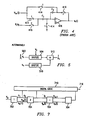
- FIG. 4 illustrates the ith stage of a conventional 1.5 bits per stage pipelined analog to digital converter.
- Each stage of a pipelined analog to digital converter consists of two nominally equal capacitors, C 1 and C 2 , and an operational amplifier 406.
- V in ( i ) is the input voltage as to stage i .
- V R represents the reference voltage sample that is being quantized in the pipelined analog to digital converter.
- V in ( i ) is compared with two levels, V + (0 ⁇ V + ⁇ V R /2) and V - (-V R /2 ⁇ V - ⁇ 0).
- Digital output D( i ) is produced according to:
- V o ( i ) the voltage output of stage i which is to be passed as V in ( i + 1) to stage i + 1 is produced.
- V o ( i ) is represented as 2V in ( i ) - D( i )V R .
- the circuit comprising the ith stage is designed with switched capacitor architecture, although a dc loop or other design could be used.
- switches 414 are turned “ON” and switches 416 are turned “OFF”, connecting the operational amplifier 406 in unity gain mode. This allows sampling of the voltage V in ( i ) on capacitors C 1 and C 2 .
- switches 414 are turned “OFF” and switches 416 are turned “ON”. Igx noring charge rejection, V o ( i ) is represented as 2V in ( i ) - D( i )V R .
- V o ( i ) When capacitor mismatch and amplifier gain error are taken into consideration, V o ( i ) is represented as where amplifier gain is represented as A i .
- the error in V o ( i ) can be approximated digitally by: where DV in ( i ) is a digital approximation of V in ( i ).
- the digital approximation of the error eliminates V R as it is a normalizing factor.
- V in (i) is assumed to be a perfect digital representation of V in (i) for the purposes of calculating DV err ( i ).
- the digital approximation of V in ( i ) is calculated using the digital results of successive stages of the pipelined analog to digital converter.
- FIG. 7 schematically depicts a 1.5 bits per stage pipelined analog to digital converter.
- Each stage 702 and 704 resolves one bit of the digital approximation of V in .
- the first stage 702 accepts the sampled voltage, V in , as input and produces a digital output of 1-bit and an output voltage, V o (1).
- V o (1) becomes V in (2) for the next stage 704 of the converter.
- the digital output, D 1 becomes the digital input D 2 for the next stage of the converter 704.
- the digital output of each stage is also input to the digital logic unit 710 for output of the self-calibrated digital approximation of the input voltage 716.
- the second and successive stages of the converter accept as input both V in ( i ) and D i and have as their output V o ( i ) for the next stage and D i for the digital logic unit and the next stage, i + 1.
- the last stage of the pipelined converter has only D i as its output as a V o ( i ) is not necessary.
- the error introduced in each stage of the pipelined analog to digital converter can be numbered starting with the most significant bit stage. This yields the following input referred error terms:
- error for each bit of the conversion again numbering from the most significant bit stage, as:
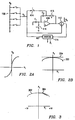
- FIG. 2A represents the voltage input range V( i ) applied to the i th stage of a pipelined analog to digital converter.
- the solid line 202 represents amplifier gain A i for an operational amplifier 416 in the ith stage of the same pipelined analog to digital converter over the given input voltage range V( i ).
- the dashed line 204 represents the output of a theoretical operational amplifier with constant gain over the same voltage input V( i ).
- Figure 3 graphically represents a digital calibration strategy for correcting amplifier gain and non-linearity.
- the amplifier's gain A i over the input voltage V( i ) is represented as a dashed line 302.
- the solid line 304 defines a digital approximation of the amplifier's gain.
- the precision of this piecewise linear approximation increases with the number of segments sampled at each stage.
- a sample of 4 segments provides for adequate precision in a 14-bit conversion.
- Two bits of resolution provides for four segments of piecewise approximation of the amplifier's gain over V( i ), the range that will be the input to the i th stage of a pipelined analog to digital converter.
- This piecewise strategy is followed for each stage of the pipelined analog to digital converter as each stage has a separate operational amplifier with separate gain and linearity characteristics.
- Figure 1 illustrates the circuit of Figure 4 configured to measure gain error at various segments of an input voltage range V( i ).
- Voltage V x is representative of a possible input voltage for a particular segment of the i th stage amplifier.
- the resistor network 108 is representative of the manner in which an input reference voltage, V R , is divided into the number of segments desired for gain error measurement.
- the measurement is produced in two phases. In phase one, switches 414 are turned “ON” and switches 416 are turned “OFF”, connecting the operational amplifier 416 in unity gain mode. This allows sampling of V x on capacitors C 1 and C 2 . In phase two, switches 414 are turned “OFF” and switches 416 are turned “ON”.
- This amplifier output is summed 112 with the original voltage V x yielding, 2V x /A i or, two times the voltage modified by any amplifier gain error.
- This result is digitized 114 using voltage V x as a reference. Therefore V x is cancelled, yielding the amplifier gain error for the given segment, represented as 1/A i .
- This process is repeated for each segment, utilizing the resistor network 108 to introduce a voltage V x representative of a voltage within the segment. The entire process is repeated for each stage of the pipelined analog to digital conversion.
- the result can be digitized 504 with the original V x subtracted out yielding V x /A i .
- the input voltage V x can be digitized 510.
- V x can then be divided 512 out of V x /A i yielding 1/A i 514, the amplifier gain error for the given segment.
- the values ⁇ i and ⁇ i can be calculated not only for a particular stage, i, of the pipelined analog to digital converter but also for segments within each stage according to:
- the values for each segment in a stage can be represented as ⁇ ij and ⁇ ij where i represents the current stage of the pipelined analog to digital converter and j represents the amplifier gain segment within the ith stage.
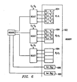
- Figure 6 represents the preferred implementation method of the digital self-calibration scheme.
- the corresponding j values are stored in a two-dimensional array 604 containing both ⁇ and ⁇ values.
- a single correction factor 606 is calculated and stored.
- the digital output of stages I + 1 to I + x is used to reference the proper row of the matrix corresponding to ⁇ i and ⁇ i .
- x the number of bits of precision used in the piecewise approximation amplifier gain correction calculation
- all possible values for all possible error terms are computed and stored in a non-volatile memory array.
- the appropriate error term is selected using the bits of the output of the pipelined analog to digital converter as addresses. While this requires a large number of initial computations and a large amount of hardware non-volatile memory space, it results in faster corrected output as only one addition operation per error term is required.
- capacitor non-linearity is extremely difficult to determine and is usually measured, if at all, at manufacture time or derived from a device model.
- a look-up table like the array 604 used to store the values for ⁇ ij and ⁇ ij , can be referenced to provide • i values for the determination of ⁇ i and ⁇ i .
- capacitor mismatch and amplifier gain errors are usually of such a minute degree that they do not manifest themselves until resolutions of more than 8 bits are attempted.
- capacitor mismatch and amplifier gain errors are usually of such a minute degree that they do not manifest themselves until resolutions of more than 8 bits are attempted.
- a 14-bit converter preferably 6 bits or stages of the pipeline are corrected.
- a greater or fewer number of bits or stages can alternatively be corrected using this technique.
- amplifier non-linearity errors typically do not manifest themselves until resolutions of more than 11 or 12 bits are attempted.
- 3 or more stages of the pipeline must be corrected.
- a greater or fewer number of bits or stages could be corrected using this technique.
- a 1-bit per stage converter can also make use of this self-calibration technique.
- analog to digital conversion architectures such as one-stage recycling converters can also make use of this self-calibration technique.
- the digital self-correction technique described can be used in combination with analog self-correction techniques.
Landscapes
- Physics & Mathematics (AREA)
- Nonlinear Science (AREA)
- Engineering & Computer Science (AREA)
- Theoretical Computer Science (AREA)
- Analogue/Digital Conversion (AREA)
Applications Claiming Priority (2)
| Application Number | Priority Date | Filing Date | Title |
|---|---|---|---|
| US156398A | 1998-01-15 | 1998-01-15 | |
| US1563P | 1998-01-15 |
Publications (2)
| Publication Number | Publication Date |
|---|---|
| EP0930715A2 true EP0930715A2 (de) | 1999-07-21 |
| EP0930715A3 EP0930715A3 (de) | 2001-01-17 |
Family
ID=21696699
Family Applications (1)
| Application Number | Title | Priority Date | Filing Date |
|---|---|---|---|
| EP99300237A Ceased EP0930715A3 (de) | 1998-01-15 | 1999-01-14 | Digitales Selbstkalibriersystem für einen Fliessband-A/D-Wandler |
Country Status (1)
| Country | Link |
|---|---|
| EP (1) | EP0930715A3 (de) |
Cited By (3)
| Publication number | Priority date | Publication date | Assignee | Title |
|---|---|---|---|---|
| US6486807B2 (en) | 2000-04-25 | 2002-11-26 | Telefonaktiebolaget Lm Ericsson | A/D converter calibration |
| US8405537B2 (en) | 2011-08-11 | 2013-03-26 | Pixart Imaging Inc. | Systems, devices and methods for capacitor mismatch error averaging in pipeline analog-to-digital converters |
| US8441378B2 (en) | 2011-08-11 | 2013-05-14 | Pixart Imaging, Inc. | Capacitor mismatch error correction in pipeline analog-to-digital converters |
Family Cites Families (2)
| Publication number | Priority date | Publication date | Assignee | Title |
|---|---|---|---|---|
| US5465092A (en) * | 1994-01-19 | 1995-11-07 | National Semiconductor Corporation | Pipelined analog-to-digital converter with curvefit digital correction |
| US5668549A (en) * | 1994-11-10 | 1997-09-16 | National Semiconductor Corporation | Radix 2 architecture and calibration technique for pipelined analog to digital converters |
-
1999
- 1999-01-14 EP EP99300237A patent/EP0930715A3/de not_active Ceased
Cited By (3)
| Publication number | Priority date | Publication date | Assignee | Title |
|---|---|---|---|---|
| US6486807B2 (en) | 2000-04-25 | 2002-11-26 | Telefonaktiebolaget Lm Ericsson | A/D converter calibration |
| US8405537B2 (en) | 2011-08-11 | 2013-03-26 | Pixart Imaging Inc. | Systems, devices and methods for capacitor mismatch error averaging in pipeline analog-to-digital converters |
| US8441378B2 (en) | 2011-08-11 | 2013-05-14 | Pixart Imaging, Inc. | Capacitor mismatch error correction in pipeline analog-to-digital converters |
Also Published As
| Publication number | Publication date |
|---|---|
| EP0930715A3 (de) | 2001-01-17 |
Similar Documents
| Publication | Publication Date | Title |
|---|---|---|
| US6222471B1 (en) | Digital self-calibration scheme for a pipelined A/D converter | |
| US4894656A (en) | Self-calibrating pipelined subranging analog-to-digital converter | |
| US6184809B1 (en) | User transparent self-calibration technique for pipelined ADC architecture | |
| US6606042B2 (en) | True background calibration of pipelined analog digital converters | |
| EP0454406B1 (de) | Mehrstufiger sigma-delta-Analog-zu-Digitalkonverter | |
| JP4532808B2 (ja) | A/dコンバータの較正 | |
| US5635937A (en) | Pipelined multi-stage analog-to-digital converter | |
| US10840934B2 (en) | Methods and apparatus for a successive approximation register analog-to-digital converter | |
| US6369744B1 (en) | Digitally self-calibrating circuit and method for pipeline ADC | |
| US10790842B1 (en) | System and method for a successive approximation analog-to-digital converter | |
| KR102636356B1 (ko) | 감소된 커패시터 어레이 dac를 이용한 sar adc에서의 오프셋 보정을 위한 방법 및 장치 | |
| US11955983B2 (en) | Error-feedback SAR-ADC | |
| JP5795729B2 (ja) | 多チャネル量子化器および量子化の方法 | |
| EP0730794B1 (de) | Effiziente architektur zur korrektur von komponentenfehlanpassungen und schaltungsnichtlinearitäten in a/d umsetzern | |
| EP1182781A2 (de) | Mehrstufiger Wandler mit Anwendung eines digitalen Zittersignals | |
| US5926123A (en) | Self calibration circuitry and algorithm for multipass analog to digital converter interstage gain correction | |
| US7545295B2 (en) | Self-calibrating digital-to-analog converter and method thereof | |
| CN110086468A (zh) | 一种非二进制逐次逼近型模数转换器的权重校准方法 | |
| US5173698A (en) | Flash analog-to-digital converter with integrating input stage | |
| US11984904B2 (en) | Analog-to-digital converter (ADC) having calibration | |
| US6198423B1 (en) | Analog-to-digital converter system having enhanced digital self-calibration | |
| EP0930715A2 (de) | Digitales Selbstkalibriersystem für einen Fliessband-A/D-Wandler | |
| EP3700092A1 (de) | Analog-digital-wandlersystem, elektronische vorrichtung und verfahren zur analog-digital-wandlung | |
| US12199628B2 (en) | Calibration system and method for SAR ADCs | |
| US6750799B1 (en) | A/D conversion technique using digital averages |
Legal Events
| Date | Code | Title | Description |
|---|---|---|---|
| PUAI | Public reference made under article 153(3) epc to a published international application that has entered the european phase |
Free format text: ORIGINAL CODE: 0009012 |
|
| AK | Designated contracting states |
Kind code of ref document: A2 Designated state(s): DE FR GB IT NL |
|
| AX | Request for extension of the european patent |
Free format text: AL;LT;LV;MK;RO;SI |
|
| PUAL | Search report despatched |
Free format text: ORIGINAL CODE: 0009013 |
|
| AK | Designated contracting states |
Kind code of ref document: A3 Designated state(s): AT BE CH CY DE DK ES FI FR GB GR IE IT LI LU MC NL PT SE |
|
| AX | Request for extension of the european patent |
Free format text: AL;LT;LV;MK;RO;SI |
|
| 17P | Request for examination filed |
Effective date: 20010717 |
|
| AKX | Designation fees paid |
Free format text: DE FR GB IT NL |
|
| 17Q | First examination report despatched |
Effective date: 20040524 |
|
| STAA | Information on the status of an ep patent application or granted ep patent |
Free format text: STATUS: THE APPLICATION HAS BEEN REFUSED |
|
| 18R | Application refused |
Effective date: 20061023 |