EP0930751A1 - Anordnung zur Symbolsynchronisierung in einem OFDM-Übertragungssystem unter Verwendung der Eigenschaften eines Kommunikationskanals - Google Patents
Anordnung zur Symbolsynchronisierung in einem OFDM-Übertragungssystem unter Verwendung der Eigenschaften eines Kommunikationskanals Download PDFInfo
- Publication number
- EP0930751A1 EP0930751A1 EP98300332A EP98300332A EP0930751A1 EP 0930751 A1 EP0930751 A1 EP 0930751A1 EP 98300332 A EP98300332 A EP 98300332A EP 98300332 A EP98300332 A EP 98300332A EP 0930751 A1 EP0930751 A1 EP 0930751A1
- Authority
- EP
- European Patent Office
- Prior art keywords
- signal
- symbol
- calculated
- accumulation value
- carriers
- Prior art date
- Legal status (The legal status is an assumption and is not a legal conclusion. Google has not performed a legal analysis and makes no representation as to the accuracy of the status listed.)
- Granted
Links
- 238000000034 method Methods 0.000 title claims description 20
- 239000000969 carrier Substances 0.000 claims abstract description 99
- 238000009825 accumulation Methods 0.000 claims abstract description 68
- 230000004044 response Effects 0.000 claims abstract description 62
- 230000005540 biological transmission Effects 0.000 claims abstract description 53
- 230000002411 adverse Effects 0.000 abstract description 2
- 238000011084 recovery Methods 0.000 abstract description 2
- 238000004364 calculation method Methods 0.000 description 22
- 238000013523 data management Methods 0.000 description 12
- 238000010586 diagram Methods 0.000 description 11
- 230000000979 retarding effect Effects 0.000 description 10
- 230000001934 delay Effects 0.000 description 6
- 239000000284 extract Substances 0.000 description 6
- 239000011159 matrix material Substances 0.000 description 6
- 238000006243 chemical reaction Methods 0.000 description 3
- 230000000694 effects Effects 0.000 description 3
- 238000005070 sampling Methods 0.000 description 3
- 230000003111 delayed effect Effects 0.000 description 2
- 230000010363 phase shift Effects 0.000 description 2
- 238000001228 spectrum Methods 0.000 description 2
- 239000013078 crystal Substances 0.000 description 1
- 230000001419 dependent effect Effects 0.000 description 1
- 238000001514 detection method Methods 0.000 description 1
- 238000000605 extraction Methods 0.000 description 1
- 230000002401 inhibitory effect Effects 0.000 description 1
- 230000000644 propagated effect Effects 0.000 description 1
- 230000008054 signal transmission Effects 0.000 description 1
- 230000005236 sound signal Effects 0.000 description 1
Images






Classifications
-
- H—ELECTRICITY
- H04—ELECTRIC COMMUNICATION TECHNIQUE
- H04L—TRANSMISSION OF DIGITAL INFORMATION, e.g. TELEGRAPHIC COMMUNICATION
- H04L25/00—Baseband systems
- H04L25/02—Details ; arrangements for supplying electrical power along data transmission lines
- H04L25/03—Shaping networks in transmitter or receiver, e.g. adaptive shaping networks
- H04L25/03006—Arrangements for removing intersymbol interference
- H04L25/03159—Arrangements for removing intersymbol interference operating in the frequency domain
-
- H—ELECTRICITY
- H04—ELECTRIC COMMUNICATION TECHNIQUE
- H04L—TRANSMISSION OF DIGITAL INFORMATION, e.g. TELEGRAPHIC COMMUNICATION
- H04L27/00—Modulated-carrier systems
- H04L27/26—Systems using multi-frequency codes
- H04L27/2601—Multicarrier modulation systems
- H04L27/2647—Arrangements specific to the receiver only
- H04L27/2655—Synchronisation arrangements
- H04L27/2662—Symbol synchronisation
-
- H—ELECTRICITY
- H04—ELECTRIC COMMUNICATION TECHNIQUE
- H04L—TRANSMISSION OF DIGITAL INFORMATION, e.g. TELEGRAPHIC COMMUNICATION
- H04L25/00—Baseband systems
- H04L25/02—Details ; arrangements for supplying electrical power along data transmission lines
- H04L25/03—Shaping networks in transmitter or receiver, e.g. adaptive shaping networks
- H04L25/03006—Arrangements for removing intersymbol interference
- H04L2025/0335—Arrangements for removing intersymbol interference characterised by the type of transmission
- H04L2025/03375—Passband transmission
- H04L2025/03414—Multicarrier
-
- H—ELECTRICITY
- H04—ELECTRIC COMMUNICATION TECHNIQUE
- H04L—TRANSMISSION OF DIGITAL INFORMATION, e.g. TELEGRAPHIC COMMUNICATION
- H04L25/00—Baseband systems
- H04L25/02—Details ; arrangements for supplying electrical power along data transmission lines
- H04L25/03—Shaping networks in transmitter or receiver, e.g. adaptive shaping networks
- H04L25/03006—Arrangements for removing intersymbol interference
- H04L2025/03433—Arrangements for removing intersymbol interference characterised by equaliser structure
- H04L2025/03439—Fixed structures
- H04L2025/03522—Frequency domain
-
- H—ELECTRICITY
- H04—ELECTRIC COMMUNICATION TECHNIQUE
- H04L—TRANSMISSION OF DIGITAL INFORMATION, e.g. TELEGRAPHIC COMMUNICATION
- H04L27/00—Modulated-carrier systems
- H04L27/26—Systems using multi-frequency codes
- H04L27/2601—Multicarrier modulation systems
- H04L27/2647—Arrangements specific to the receiver only
- H04L27/2655—Synchronisation arrangements
- H04L27/2657—Carrier synchronisation
-
- H—ELECTRICITY
- H04—ELECTRIC COMMUNICATION TECHNIQUE
- H04L—TRANSMISSION OF DIGITAL INFORMATION, e.g. TELEGRAPHIC COMMUNICATION
- H04L27/00—Modulated-carrier systems
- H04L27/26—Systems using multi-frequency codes
- H04L27/2601—Multicarrier modulation systems
- H04L27/2647—Arrangements specific to the receiver only
- H04L27/2655—Synchronisation arrangements
- H04L27/2668—Details of algorithms
- H04L27/2673—Details of algorithms characterised by synchronisation parameters
- H04L27/2676—Blind, i.e. without using known symbols
- H04L27/2679—Decision-aided
Definitions
- This invention relates to a method of receiving an orthogonal frequency division multiplexed (OFDM) signal.
- This invention also relates to an apparatus for receiving an orthogonal frequency division multiplexed (OFDM) signal.
- OFDM orthogonal frequency division multiplexing
- Examples of digital information signals handled by such OFDM-based transmitting systems are multi-value modulation signals or 256-QAM (quadrature amplitude modulation) signals.
- OFDM-based transmission is good in suppressing multipath effects and jamming signal effects. Further, the OFDM-based transmission has a good efficiency of frequency use.
- Orthogonal frequency division multiplexing employs multiple carriers which are orthogonal with respect to each other.
- the multiple carriers are modulated in accordance with digital information pieces to be transmitted, respectively.
- the modulation-resultant multiple carriers are combined into an OFDM signal which has a form as a random signal.
- IFFT inverse fast Fourier transform
- the "orthogonal" multiple carriers mean that the spectrums of carriers neighboring one carrier are null at the frequency of the latter carrier.
- OFDM orthogonal frequency division multiplexed
- OFDM orthogonal frequency division multiplexed
- a first object of this invention provides a method of receiving an orthogonal frequency division multiplexed (OFDM) signal containing information and a reference signal, the method comprising the steps of receiving an OFDM signal via a transmission line; generating a symbol sync signal in response to the received OFDM signal; setting a time window for every symbol in response to the generated symbol sync signal; extracting a time segment of the received OFDM signal which extends in the time window; subjecting the extracted time segment of the received OFDM signal to discrete Fourier transform to recover transmitted information and a reference signal; periodically calculating coefficients representative of characteristics of the transmission line from the recovered reference signal; periodically calculating approximate phase differences between carriers in respective pairs among carriers of the received OFDM signal on the basis of the calculated coefficients; periodically calculating an accumulation value of the calculated approximate phase differences; comparing the currently-calculated accumulation value and the previously-calculated accumulation value; and controlling the phase of the time window relative to a symbol in response to a result of the comparison between the currently-calculated accumulation value and the previously-calcul
- a second aspect of this invention provides a method of receiving an orthogonal frequency division multiplexed (OFDM) signal containing information, a symbol order number signal, and a reference signal, the symbol order number signal representing a relation between the OFDM signal and the reference signal, the method comprising the steps of receiving an OFDM signal via a transmission line; generating a symbol sync signal in response to the received OFDM signal; setting a time window for every symbol in response to the generated symbol sync signal; extracting a time segment of the received OFDM signal which extends in the time window; subjecting the extracted time segment of the received OFDM signal to discrete Fourier transform to recover transmitted information and a symbol order number signal; recovering a reference signal from a result of the discrete Fourier transform in response to the symbol order number signal; periodically calculating coefficients representative of characteristics of the transmission line from the recovered reference signal, the calculated coefficients including coefficients which indicate a rate of information transfer from a real part of a transmitter-side carrier to a real part of a receiver-side carrier, a rate of
- a third aspect of this invention provides an apparatus for receiving an orthogonal frequency division multiplexed (OFDM) signal containing information and a reference signal, the apparatus comprising means for receiving an OFDM signal via a transmission line; means for generating a symbol sync signal in response to the received OFDM signal; means for setting a time window for every symbol in response to the generated symbol sync signal; means for extracting a time segment of the received OFDM signal which extends in the time window; means for subjecting the extracted time segment of the received OFDM signal to discrete Fourier transform to recover transmitted information and a reference signal; means for periodically calculating coefficients representative of characteristics of the transmission line from the recovered reference signal; means for periodically calculating approximate phase differences between carriers in respective pairs among carriers of the received OFDM signal on the basis of the calculated coefficients; means for periodically calculating an accumulation value of the calculated approximate phase differences; means for comparing the currently-calculated accumulation value and the previously-calculated accumulation value; and means for controlling the phase of the time window relative to a symbol in response to a result of the
- a fourth aspect of this invention provides an apparatus for receiving an orthogonal frequency division multiplexed (OFDM) signal containing information, a symbol order number signal, and a reference signal, the symbol order number signal representing a relation between the OFDM signal and the reference signal, the apparatus comprising means for receiving an OFDM signal via a transmission line; means for generating a symbol sync signal in response to the received OFDM signal; means for setting a time window for every symbol in response to the generated symbol sync signal; means for extracting a time segment of the received OFDM signal which extends in the time window; means for subjecting the extracted time segment of the received OFDM signal to discrete Fourier transform to recover transmitted information and a symbol order number signal; means for recovering a reference signal from a result of the discrete Fourier transform in response to the symbol order number signal; means for periodically calculating coefficients representative of characteristics of the transmission line from the recovered reference signal, the calculated coefficients including coefficients which indicate a rate of information transfer from a real part of a transmitter-side carrier to a real part of
- a baseband OFDM signal is composed of multiple orthogonal baseband carriers which have been modulated in accordance with transmitted information pieces respectively.
- the baseband OFDM signal has a time-base waveform such as shown in Fig. 1.
- each OFDM transmission symbol interval "ta” is composed of a guard interval "gi” and an effective symbol interval "ts".
- the guard interval "gi” precedes the effective symbol interval "ts”.
- the guard interval "gi” is used for reducing multipath effects.
- the effective symbol interval "ts” is used for transmitting information (data).
- the waveform of a time segment of an OFDM signal transmitted during the guard interval "gi” is a copy of a part (for example, an end part or a later part) of the waveform of a time segment of the OFDM signal transmitted during the effective symbol interval "ts".
- the frequency intervals between the multiple carriers in the baseband OFDM signal are equal to the reciprocal of the effective symbol interval "ts".
- a transmitter side subjects N complex-number data pieces to N-point IDFT (inverse discrete Fourier transform) in frequency domain for every symbol interval "ta”. Thereby, the transmitter side generates every 1-symbol-corresponding time segment of a baseband OFDM signal containing the data pieces.
- a receiver side repetitively samples a baseband OFDM signal at a period equal to the effective symbol interval "ts" divided by N, and thereby generates N samples of the baseband OFDM signal for every symbol interval "ta".
- the receiver side subjects the N signal samples to N-point DFT (discrete Fourier transform) for every symbol interval "ta", calculating the phases and the amplitudes of respective carrier components and thereby recovering N complex-number data pieces.
- N-point DFT discrete Fourier transform
- the receiver side sets a time window for every symbol interval "ta".
- the time window is referred to as the DFT window.
- the receiver side implements DFT on signal samples available in each DFT window.
- the receiver side designates the time position of each DFT window relative to the corresponding symbol interval "ta" in response to a symbol sync signal.
- An example of a way of generating a symbol sync signal uses the following technique. Spaced symbols occurring at a given period are used as null symbols (signal-less intervals). A symbol sync signal is recovered in response to the null symbols. Generally, a recovered symbol sync signal is allowed to have an error of less than several samples with respect to the boundaries between symbols.
- a receiver side receives a desired wave and also a ghost wave which delays from the desired wave as shown in Fig. 3.
- a symbol sync signal "sa” is generated which has a train of pulses equal in timing with starting moments "a” of effective symbol intervals "ts” of the desired wave.
- a DFT window is designated in response to each pulse of the symbol sync signal "sa”. For every symbol, signal sampling is started at the starting moment "a” of an effective symbol interval "ts", and is continued until the DFT window terminates (that is, the effective symbol interval "ts” terminates). For every symbol, DFT is implemented on signal samples available in the DFT window.
- every symbol interval "ta” starts at moments "b".
- a symbol “n” in the desired wave does not receive interference from a preceding symbol "n-1" during the interval between the related moments "b” and “a”.
- the symbol sync signal "sa” may be replaced by a symbol sync signal "sb” which has a train of pulses equal in timing with the starting moments "b” of symbol intervals "ta” of the ghost wave.
- another symbol sync signal is useful which has a train of pulses equal in timing with given points between the moments "b” and "a”.
- Such coefficients related to different carriers have a non-linear relation with each other. Accordingly, the simple mean value among the coefficients deviates from a correct value for the characteristics of the transmission line. Such a relation among coefficients related to different carriers depends on, for example, errors of symbol sync positions.
- an n-th carrier In an OFDM signal generated by 512-point IFFT, an n-th carrier has "n" periods during every effective symbol interval "ts". In other words, the n-th carrier has a phase change of 2 ⁇ n radians for every effective symbol interval "ts". Thus, the n-th carrier has a phase change of (2 ⁇ n)/512 radians for every sample. Accordingly, if there is a one-sample error, it is desirable to correct the phase of the n-th carrier by (2 ⁇ n)/512.
- An (n+1)-th carrier has "n+1" periods during every effective symbol interval "ts”. In other words, the (n+1)-th carrier has a phase change of 2 ⁇ (n+1) radians for every effective symbol interval "ts".
- the IDFT device 4 outputs the multiplexing-resultant signal corresponding to the real part. Also, the IDFT device 4 combines the 248 modulation-resultant signals and other modulation-resultant signals of the imaginary part into a multiplexing-resultant signal corresponding to the imaginary part. The IDFT device 4 outputs the multiplexing-resultant signal corresponding to the imaginary part.
- the 248 output signals from the input circuit 2 in each of the real part and the imaginary part are transmitted by the 248 carriers respectively.
- I +10 (S0 +10 ⁇ S1 +20 - S0 +20 ⁇ S1 +10 )/(S0 +10 ⁇ S0 +20 + S1 +10 ⁇ S1 +20 )
- the calculation circuit 314 calculates the phase difference I -10 between the 10-th negative carrier and the 20-th negative carrier according to the following approximate equation.
- I -10 (S6 -10 ⁇ S7 -20 - S6 -20 ⁇ S7 -10 )/(S6 -10 ⁇ S6 -20 + S7 -10 ⁇ S7 -20 )
- the calculation circuit 314 calculates the phase difference I +X between the X-th positive carrier and the (X+10)-th positive carrier according to the following approximate equation.
- I -X (S6 -X ⁇ S7 -X-10 - S6 -X-10 ⁇ S7 -X )/(S6 -X ⁇ S6 -X-10 + S7 -X ⁇ S7 -X-10 )
- the calculation circuit 314 outputs information representative of the calculated accumulation value I to the control circuit 313.
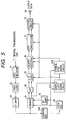
- the adjustment circuit 302 includes a counter which counts pulses of the sample clock signal fed from the sample clock signal generating circuit 27A (see Fig. 5).
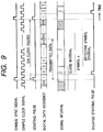
- An example of the waveform of the sample clock signal is shown in Fig. 9.
- the count number provided by the counter in the adjustment circuit 302 is reset or cleared by every pulse of the symbol sync signal fed from the symbol sync signal generating circuit 27B (see Fig. 5).
- An example of the waveform of the symbol sync signal is shown in Fig. 9.
- the count number is incremented one by one in response to every pulse of the sample clock signal.
- the adjustment circuit 302 outputs a starting pulse to the data management circuit 301.
- An example of the waveform of the starting pulse is shown in Fig. 9.
- Every symbol corresponds to 524 digital signal time segments (524 samples) composed of 512 effective digital signal time segments (512 effective samples) and 12 digital signal time segments (12 samples) for a guard interval.
- a sequence of 512 digital signal time segments (512 samples) which starts from the moment of the occurrence of a starting pulse is transmitted from the A/D converter 29 to the DFT QAM decoding circuit 31 through the data management circuit 301 as data time segments available in a DFT window.
- 12 remaining digital signal time segments are inhibited by the data management circuit 301 from traveling to the DFT QAM decoding circuit 31.
- digital signal time segments numbered as “1”, “2", ⁇ , and "512" are transmitted while digital signal time segments numbered as "513", "514", ⁇ , and "524" are blocked.
- the data management circuit 301 responds to the delayed starting pulse, thereby permitting the transmission of digital signal time segments numbered as “2", “3”, ⁇ , and “513” and inhibiting the transmission of digital signal time segments numbered as "514", "515", ⁇ , "524", and "1".
- the accumulation value I provided by the calculation circuit 314 in the DFT QAM decoding circuit 31 is minimized when the time position of the starting pulse comes into agreement with the time position of the end of the guard interval "gi".
- the accumulation value I increases as the time position of the starting pulse enters the effective symbol interval "ts" and retards from the time position of the end of the guard interval "gi". Also, the accumulation value I increases as the time position of the starting pulse advances from the time position of the end of the guard interval "gi" toward the time position of the head thereof.
- the adjustment circuit 302 delays the starting pulse so that the DFT window also delays relative to the symbol interval "ta".
- the DFT QAM decoding circuit 31 outputs the retarding pulse to the adjustment circuit 302 instead of the advancing pulse. It is thought that the starting pulse which occurs immediately before its entrance into the effective symbol interval "ts" is correct in timing with respect to the effective symbol interval "ts". To recover such a correct starting pulse, the retarding pulse is generated instead of the advancing pulse.
- the adjustment circuit 302 When the retarding pulse is fed from the DFT QAM decoding circuit 31, the adjustment circuit 302 adds one pulse to 524 successive pulses of the sample clock signal. Therefore, the adjustment circuit 302 outputs an advanced starting pulse which is advanced by a time interval corresponding to one pulse of the sample clock signal.
- the data management circuit 301 responds to the advanced starting pulse, thereby permitting the transmission of digital signal time segments advanced by one sample. As a result, the DFT window is advanced back into substantial agreement with the effective symbol interval "ts". During a later stage, the DFT window is held in substantial agreement with the effective symbol interval "ts".
- the output signal of the frequency divider 3021 is periodically written into a given storage location (for example, a first storage location) in the shift register 3022 in response to the sample clock signal fed from the sample clock signal generating circuit 27A (see Fig. 5).
- a given storage location for example, a first storage location
- 1-bit signals are moved from the storage locations to the adjacent storage locations in response to every pulse in the sample clock signal.
- the shift register 3022 periodically implements a signal shifting process in response to the sample clock signal.
- the shift register 3022 outputs an 8-bit parallel-form signal from the 8 storage locations to the selector 3023 which periodically varies in accordance with the signal shifting process.
- the selector 3023 has an "up" terminal and a “down” terminal to which the advancing pulse and the retarding pulse can be applied from the DFT QAM decoding circuit 31 respectively.
- the selector 3023 selects one from among the 8 bits of the output signal of the shift register 3022 as a starting pulse.
- the selector 3023 selects one from among the 8 bits whose phase delays from the phase of the previously-selected bit by one sample.
- the selector 3023 selects one from among the 8 bits whose phase advances from the phase of the previously-selected bit by one sample.
- the selector 3023 outputs the selected bit to the data management circuit 301 as a starting pulse for every symbol.
- the control circuit 313 and the calculation circuit 314 in the DFT QAM decoding circuit 31 include a common CPU which operates in accordance with a program stored in its internal ROM.
- Fig. 11 is a flowchart of the program. The program is started when the signal receiving apparatus of Fig. 5 is turned on. The program remains executed during an initial stage immediately after the signal receiving apparatus of Fig. 5 is turned on. Specifically, the program remains executed until a retarding pulse is outputted instead of an advancing pulse, that is, until the DFT window is made into substantial agreement with the effective symbol interval "ts".
- a first step 42 of the program decides whether or not one new cycle of the symbol order number has been completed, that is, whether or not a new 1-frame interval has elapsed, by referring to the symbol order number signal.
- the program advances from the step 42 to a step 43. Otherwise, the program repeats the step 42.
- a step 44 following the step 43 decides whether or not the execution of the step 43, that is, the calculation of the accumulation value I, is the first time.
- the program returns to the step 42.
- the program advances from the step 44 to a step 45.
- the step 46 outputs an advancing pulse to the guard interval processing circuit 30. After the step 46, the program returns to the step 42.
- each OFDM transmission symbol interval "ta” may be composed of a pre-guard-interval "C", an effective symbol interval "B", and a post-guard-interval "A".
- the pre-guard-interval "C” precedes the effective symbol interval "B”.
- the post-guard-interval "A” follows the effective symbol interval "B”.
- the effective symbol interval "B” contains 512 digital data pieces (512 samples).
- the pre-guard-interval "C” contains 10 digital data pieces (10 samples) which are copies of 10 later digital data pieces among the 512 digital dat pieces assigned to the effective symbol interval "B”.
- the post-guard interval "A” contains 2 digital data pieces (2 samples) which are copies of 2 former digital data pieces among the 512 digital data pieces assigned to the effective symbol interval "B".
Landscapes
- Engineering & Computer Science (AREA)
- Computer Networks & Wireless Communication (AREA)
- Signal Processing (AREA)
- Power Engineering (AREA)
- Synchronisation In Digital Transmission Systems (AREA)
Priority Applications (2)
| Application Number | Priority Date | Filing Date | Title |
|---|---|---|---|
| DE69819673T DE69819673T2 (de) | 1998-01-19 | 1998-01-19 | Anordnung zur Symbolsynchronisierung in einem OFDM-Übertragungssystem unter Verwendung der Eigenschaften eines Kommunikationskanals |
| EP98300332A EP0930751B1 (de) | 1998-01-19 | 1998-01-19 | Anordnung zur Symbolsynchronisierung in einem OFDM-Übertragungssystem unter Verwendung der Eigenschaften eines Kommunikationskanals |
Applications Claiming Priority (1)
| Application Number | Priority Date | Filing Date | Title |
|---|---|---|---|
| EP98300332A EP0930751B1 (de) | 1998-01-19 | 1998-01-19 | Anordnung zur Symbolsynchronisierung in einem OFDM-Übertragungssystem unter Verwendung der Eigenschaften eines Kommunikationskanals |
Publications (2)
| Publication Number | Publication Date |
|---|---|
| EP0930751A1 true EP0930751A1 (de) | 1999-07-21 |
| EP0930751B1 EP0930751B1 (de) | 2003-11-12 |
Family
ID=8234626
Family Applications (1)
| Application Number | Title | Priority Date | Filing Date |
|---|---|---|---|
| EP98300332A Expired - Lifetime EP0930751B1 (de) | 1998-01-19 | 1998-01-19 | Anordnung zur Symbolsynchronisierung in einem OFDM-Übertragungssystem unter Verwendung der Eigenschaften eines Kommunikationskanals |
Country Status (2)
| Country | Link |
|---|---|
| EP (1) | EP0930751B1 (de) |
| DE (1) | DE69819673T2 (de) |
Cited By (3)
| Publication number | Priority date | Publication date | Assignee | Title |
|---|---|---|---|---|
| GB2364221A (en) * | 2000-03-15 | 2002-01-16 | Mitsubishi Electric Corp | Clock recovery circuit and method for OFDM |
| GB2398468A (en) * | 2003-02-15 | 2004-08-18 | 4I2I Comm Ltd | Aligning a received OFDM signal with a reference signal |
| CN105407062A (zh) * | 2014-09-15 | 2016-03-16 | 联咏科技股份有限公司 | 检测正交分频多工信号的保护间隔的装置及其检测方法 |
Families Citing this family (2)
| Publication number | Priority date | Publication date | Assignee | Title |
|---|---|---|---|---|
| KR100566201B1 (ko) * | 2002-04-22 | 2006-03-29 | 삼성전자주식회사 | 직교 주파수 분할 다중 접속 방식을 사용하는 이동 통신시스템에서 레인징 방법 |
| DE102016201991B4 (de) | 2015-02-12 | 2023-10-12 | Mitsubishi Electric Corporation | Synchronisationszeit-Steuervorrichtung, Synchronisationszeit-Steuerverfahren und Empfänger |
Citations (7)
| Publication number | Priority date | Publication date | Assignee | Title |
|---|---|---|---|---|
| EP0453203A2 (de) * | 1990-04-16 | 1991-10-23 | Telebit Corporation | Verfahren und Einrichtung zum Korrigieren der Takt- und Trägerfrequenzschiebung und des Phasen-Jitters in Mehrträgermodems |
| EP0683576A1 (de) * | 1994-05-20 | 1995-11-22 | Hitachi, Ltd. | Digitales OFDM-Rundfunksystem, sowie Übertragungs- und Empfangsvorrichtung für Digitalrundfunk |
| WO1996019056A1 (en) * | 1994-12-14 | 1996-06-20 | Hd Divine | Method at ofdm-reception for correction of frequency, time window, sampling clock and slow phase variations |
| EP0736986A1 (de) * | 1995-03-31 | 1996-10-09 | Sony Corporation | Datenempfangssystem, Datenübertragungssystem und geeignetes Verfahren, welche im Übertragungssignal eingefügten Bezugsdaten verwenden, um die Qualität des Übertragungskanals abzuschätzen |
| EP0765059A2 (de) * | 1995-09-25 | 1997-03-26 | Victor Company Of Japan, Limited | Verfahren zur Übertragung eines orthogonalen Frequenzmultiplexsignals (OFDM) und Sender/Empfänger dafür |
| EP0795985A2 (de) * | 1996-03-13 | 1997-09-17 | NOKIA TECHNOLOGY GmbH | Ausgleich von Phasenfehlern in Mehrträgersignalen |
| WO1998010547A2 (en) * | 1996-09-02 | 1998-03-12 | Telia Ab | Improvements in, or relating to, multi-carrier transmission systems |
-
1998
- 1998-01-19 EP EP98300332A patent/EP0930751B1/de not_active Expired - Lifetime
- 1998-01-19 DE DE69819673T patent/DE69819673T2/de not_active Expired - Lifetime
Patent Citations (7)
| Publication number | Priority date | Publication date | Assignee | Title |
|---|---|---|---|---|
| EP0453203A2 (de) * | 1990-04-16 | 1991-10-23 | Telebit Corporation | Verfahren und Einrichtung zum Korrigieren der Takt- und Trägerfrequenzschiebung und des Phasen-Jitters in Mehrträgermodems |
| EP0683576A1 (de) * | 1994-05-20 | 1995-11-22 | Hitachi, Ltd. | Digitales OFDM-Rundfunksystem, sowie Übertragungs- und Empfangsvorrichtung für Digitalrundfunk |
| WO1996019056A1 (en) * | 1994-12-14 | 1996-06-20 | Hd Divine | Method at ofdm-reception for correction of frequency, time window, sampling clock and slow phase variations |
| EP0736986A1 (de) * | 1995-03-31 | 1996-10-09 | Sony Corporation | Datenempfangssystem, Datenübertragungssystem und geeignetes Verfahren, welche im Übertragungssignal eingefügten Bezugsdaten verwenden, um die Qualität des Übertragungskanals abzuschätzen |
| EP0765059A2 (de) * | 1995-09-25 | 1997-03-26 | Victor Company Of Japan, Limited | Verfahren zur Übertragung eines orthogonalen Frequenzmultiplexsignals (OFDM) und Sender/Empfänger dafür |
| EP0795985A2 (de) * | 1996-03-13 | 1997-09-17 | NOKIA TECHNOLOGY GmbH | Ausgleich von Phasenfehlern in Mehrträgersignalen |
| WO1998010547A2 (en) * | 1996-09-02 | 1998-03-12 | Telia Ab | Improvements in, or relating to, multi-carrier transmission systems |
Non-Patent Citations (1)
| Title |
|---|
| DATABASE WPI Section EI Week 9817, Derwent World Patents Index; Class W01, AN 98-193992, XP002072200 * |
Cited By (7)
| Publication number | Priority date | Publication date | Assignee | Title |
|---|---|---|---|---|
| GB2364221A (en) * | 2000-03-15 | 2002-01-16 | Mitsubishi Electric Corp | Clock recovery circuit and method for OFDM |
| GB2364221B (en) * | 2000-03-15 | 2002-08-28 | Mitsubishi Electric Corp | Clock recovery circuit and method |
| GB2398468A (en) * | 2003-02-15 | 2004-08-18 | 4I2I Comm Ltd | Aligning a received OFDM signal with a reference signal |
| GB2398468B (en) * | 2003-02-15 | 2007-09-05 | 4I2I Comm Ltd | Synchronisation method and apparatus for OFDM symbols |
| US7697617B2 (en) | 2003-02-15 | 2010-04-13 | 4I2I Communications Limited | Synchronisation method and apparatus for OFDM symbols |
| CN105407062A (zh) * | 2014-09-15 | 2016-03-16 | 联咏科技股份有限公司 | 检测正交分频多工信号的保护间隔的装置及其检测方法 |
| CN105407062B (zh) * | 2014-09-15 | 2019-02-12 | 联咏科技股份有限公司 | 检测正交分频多工信号的保护间隔的装置及其检测方法 |
Also Published As
| Publication number | Publication date |
|---|---|
| DE69819673D1 (de) | 2003-12-18 |
| EP0930751B1 (de) | 2003-11-12 |
| DE69819673T2 (de) | 2004-09-30 |
Similar Documents
| Publication | Publication Date | Title |
|---|---|---|
| EP0822691B1 (de) | Rückgewinnung des Symboltaktes in einem Empfänger für Mehrträgersignale | |
| US7421029B2 (en) | Impulse response shortening and symbol synchronization in OFDM communication systems | |
| EP0712555B1 (de) | Verfahren und einrichtung zur synchronisierung in digitalen ofdm-übertragungssystemen | |
| EP0982908B1 (de) | Einstellung eines Referenzunterträgers bei Mehrträgerübertragung | |
| KR100736062B1 (ko) | 직교 주파수 분할 다중화 시스템에서의 샘플링 주파수 오프셋의 정정 | |
| EP0929172B1 (de) | System zur Mehrträgermodulation, mit veränderbaren Symbolgeschwindigkeiten | |
| US6704374B1 (en) | Local oscillator frequency correction in an orthogonal frequency division multiplexing system | |
| KR100263372B1 (ko) | 직교분할대역 시스템의 간략 주파수 획득 방법 및 그 장치 | |
| US6711221B1 (en) | Sampling offset correction in an orthogonal frequency division multiplexing system | |
| US6584164B1 (en) | Method for forming a training sequence | |
| US6252908B1 (en) | Method and device in a communication system | |
| EP0765059B1 (de) | Verfahren zur Übertragung eines orthogonalen Frequenzmultiplexsignals (OFDM) und Sender/Empfänger dafür | |
| US5822323A (en) | Frequency division multiplexed signal generating apparatus and related decoding apparatus | |
| JPH0746218A (ja) | ディジタル復調装置 | |
| US6961393B1 (en) | In-band-on-channel (IBOC) system and methods of operation using orthogonal frequency division multiplexing (OFDM) with timing and frequency offset correction | |
| EP2566123B1 (de) | Ausgleichsvorrichtungen und verfahren zum erkennen und ausgleichen von abtasttaktverschiebungen | |
| KR100213100B1 (ko) | Ofdm 전송 신호의 주파수 오류 정정기와 그 방법 | |
| EP0991238B1 (de) | Erzeugung und Decodierung eines Mehrträgersignals | |
| EP0930751B1 (de) | Anordnung zur Symbolsynchronisierung in einem OFDM-Übertragungssystem unter Verwendung der Eigenschaften eines Kommunikationskanals | |
| WO1997041672A1 (en) | Symbol synchronisation in a multicarrier receiver | |
| US20060165187A1 (en) | Multiplex signal error correction method and device | |
| EP1006699B1 (de) | Synchronisierung von Symbolen bei Mehrträgerübertragung | |
| JP3700290B2 (ja) | 直交周波数分割多重信号伝送方法及びそれに用いる受信装置 | |
| EP2159981A2 (de) | Empfangsvorrichtung und -verfahren zum Empfang von OFDM-Signalen | |
| US7065171B1 (en) | Method for synchronization of received signals |
Legal Events
| Date | Code | Title | Description |
|---|---|---|---|
| PUAI | Public reference made under article 153(3) epc to a published international application that has entered the european phase |
Free format text: ORIGINAL CODE: 0009012 |
|
| 17P | Request for examination filed |
Effective date: 19981007 |
|
| AK | Designated contracting states |
Kind code of ref document: A1 Designated state(s): AT BE CH DE DK ES FI FR GB GR IE IT LI LU MC NL PT SE |
|
| AX | Request for extension of the european patent |
Free format text: AL;LT;LV;MK;RO;SI |
|
| AKX | Designation fees paid |
Free format text: DE FR GB |
|
| GRAH | Despatch of communication of intention to grant a patent |
Free format text: ORIGINAL CODE: EPIDOS IGRA |
|
| GRAS | Grant fee paid |
Free format text: ORIGINAL CODE: EPIDOSNIGR3 |
|
| GRAA | (expected) grant |
Free format text: ORIGINAL CODE: 0009210 |
|
| AK | Designated contracting states |
Kind code of ref document: B1 Designated state(s): DE FR GB |
|
| REG | Reference to a national code |
Ref country code: GB Ref legal event code: FG4D |
|
| REF | Corresponds to: |
Ref document number: 69819673 Country of ref document: DE Date of ref document: 20031218 Kind code of ref document: P |
|
| ET | Fr: translation filed | ||
| PLBE | No opposition filed within time limit |
Free format text: ORIGINAL CODE: 0009261 |
|
| STAA | Information on the status of an ep patent application or granted ep patent |
Free format text: STATUS: NO OPPOSITION FILED WITHIN TIME LIMIT |
|
| 26N | No opposition filed |
Effective date: 20040813 |
|
| REG | Reference to a national code |
Ref country code: DE Ref legal event code: R082 Ref document number: 69819673 Country of ref document: DE Representative=s name: MANITZ, FINSTERWALD & PARTNER GBR, DE |
|
| REG | Reference to a national code |
Ref country code: DE Ref legal event code: R082 Ref document number: 69819673 Country of ref document: DE Representative=s name: MANITZ FINSTERWALD PATENTANWAELTE PARTMBB, DE Effective date: 20120430 Ref country code: DE Ref legal event code: R082 Ref document number: 69819673 Country of ref document: DE Representative=s name: MANITZ, FINSTERWALD & PARTNER GBR, DE Effective date: 20120430 Ref country code: DE Ref legal event code: R081 Ref document number: 69819673 Country of ref document: DE Owner name: JVC KENWOOD CORPORATION, JP Free format text: FORMER OWNER: VICTOR COMPANY OF JAPAN, LTD., YOKOHAMA, JP Effective date: 20120430 Ref country code: DE Ref legal event code: R081 Ref document number: 69819673 Country of ref document: DE Owner name: JVC KENWOOD CORPORATION, YOKOHAMA-SHI, JP Free format text: FORMER OWNER: VICTOR COMPANY OF JAPAN, LTD., YOKOHAMA, KANAGAWA, JP Effective date: 20120430 |
|
| REG | Reference to a national code |
Ref country code: FR Ref legal event code: TP Owner name: JVC KENWOOD CORPORATION, JP Effective date: 20120705 |
|
| REG | Reference to a national code |
Ref country code: FR Ref legal event code: PLFP Year of fee payment: 19 |
|
| REG | Reference to a national code |
Ref country code: FR Ref legal event code: PLFP Year of fee payment: 20 |
|
| PGFP | Annual fee paid to national office [announced via postgrant information from national office to epo] |
Ref country code: FR Payment date: 20161215 Year of fee payment: 20 |
|
| PGFP | Annual fee paid to national office [announced via postgrant information from national office to epo] |
Ref country code: DE Payment date: 20170110 Year of fee payment: 20 |
|
| PGFP | Annual fee paid to national office [announced via postgrant information from national office to epo] |
Ref country code: GB Payment date: 20170118 Year of fee payment: 20 |
|
| REG | Reference to a national code |
Ref country code: DE Ref legal event code: R071 Ref document number: 69819673 Country of ref document: DE |
|
| REG | Reference to a national code |
Ref country code: GB Ref legal event code: PE20 Expiry date: 20180118 |
|
| PG25 | Lapsed in a contracting state [announced via postgrant information from national office to epo] |
Ref country code: GB Free format text: LAPSE BECAUSE OF EXPIRATION OF PROTECTION Effective date: 20180118 |