EP0931379B1 - Pompe a charge avec trois puits - Google Patents
Pompe a charge avec trois puits Download PDFInfo
- Publication number
- EP0931379B1 EP0931379B1 EP96939448A EP96939448A EP0931379B1 EP 0931379 B1 EP0931379 B1 EP 0931379B1 EP 96939448 A EP96939448 A EP 96939448A EP 96939448 A EP96939448 A EP 96939448A EP 0931379 B1 EP0931379 B1 EP 0931379B1
- Authority
- EP
- European Patent Office
- Prior art keywords
- transistor
- charge pump
- transistors
- well
- source
- Prior art date
- Legal status (The legal status is an assumption and is not a legal conclusion. Google has not performed a legal analysis and makes no representation as to the accuracy of the status listed.)
- Expired - Lifetime
Links
Images


Classifications
-
- H—ELECTRICITY
- H10—SEMICONDUCTOR DEVICES; ELECTRIC SOLID-STATE DEVICES NOT OTHERWISE PROVIDED FOR
- H10D—INORGANIC ELECTRIC SEMICONDUCTOR DEVICES
- H10D89/00—Aspects of integrated devices not covered by groups H10D84/00 - H10D88/00
- H10D89/211—Design considerations for internal polarisation
- H10D89/213—Design considerations for internal polarisation in field-effect devices
- H10D89/215—Design considerations for internal polarisation in field-effect devices comprising arrangements for charge pumping or biasing substrates
-
- H—ELECTRICITY
- H02—GENERATION; CONVERSION OR DISTRIBUTION OF ELECTRIC POWER
- H02M—APPARATUS FOR CONVERSION BETWEEN AC AND AC, BETWEEN AC AND DC, OR BETWEEN DC AND DC, AND FOR USE WITH MAINS OR SIMILAR POWER SUPPLY SYSTEMS; CONVERSION OF DC OR AC INPUT POWER INTO SURGE OUTPUT POWER; CONTROL OR REGULATION THEREOF
- H02M3/00—Conversion of DC power input into DC power output
- H02M3/02—Conversion of DC power input into DC power output without intermediate conversion into AC
- H02M3/04—Conversion of DC power input into DC power output without intermediate conversion into AC by static converters
- H02M3/06—Conversion of DC power input into DC power output without intermediate conversion into AC by static converters using resistors or capacitors, e.g. potential divider
- H02M3/07—Conversion of DC power input into DC power output without intermediate conversion into AC by static converters using resistors or capacitors, e.g. potential divider using capacitors charged and discharged alternately by semiconductor devices with control electrode, e.g. charge pumps
- H02M3/073—Charge pumps of the Schenkel-type
Definitions
- the present invention relates to charge pump circuits, and more particularly to using triple well transistors in the design of charge pump circuits.
- a charge pump is a circuit that can generate an output voltage that is higher than the voltage supplied to the charge pump.
- One of the applications of charge pumps is to develop voltage for erasing and programming some kinds of nonvolatile semiconductor memory devices, such as electrical erasable programmable read only memory (EEPROM) and flash memory.
- EEPROM electrical erasable programmable read only memory
- One way to operate these memory devices is to program through hot electron injection and erase through Fowler-Nordheim tunneling. The programming and erasing of such a memory cell require current to pass through the dielectric surrounding a floating gate electrode. As a result, a high voltage is generally needed.
- Some prior art nonvolatile semiconductor memory devices require the application of an external high voltage (e.g, 12 volts) in addition to a regular 5 volts supply voltage.
- US-A-5 489 870 discloses a voltage booster circuit.
- Charge transfer transistors are provided which cause charge to be transferred from one stage to the next in order to boost the voltage.
- Additional, separate, transistors are provided to reduce the susceptibility of the threshold voltage of the charge transfer transistors to the back bias effect.
- a charge pump comprising a semiconductor body having a particular conductivity type; a first well in said semiconductor body having said particular conductivity type; a second well in said semiconductor body surrounding said first well and having an opposite conductivity type relative to the particular conductivity type; a plurality of transistors, each of the transistors in the plurality having a source terminal and a drain terminal, the plurality of transistors arranged in series from a first transistor in the series coupled to a power supply voltage (V DD ; GND) to a last transistor in the plurality coupled to an output of the charge pump, to pump a voltage level of said output of the charge pump in response to one or more clock pulses, said last transistor having a voltage level substantially higher than, for a positive voltage output, or negative relative to, for a negative voltage output, said power supply voltage, the plurality of transistors in the series being connected such that, for a positive voltage output, the source of one of the transistors in the series is connected to the drain of a preceding transistor in the
- Embodiments of the present invention relate to using triple well transistors to increase the efficiency of a charge pump.
- the inventive charge pump comprises a plurality of pumping transistors arranged to increase the voltage level from a first pumping transistor to a last pumping transistor in response to clock pulses applied to these pumping transistors.
- At least one of the plurality of pumping transistors has a source and a drain region of a first conductive type formed on a first well having an opposite conductive type.
- a second well having the first conductive type can be formed outside of the first well.
- the second well is fabricated on a substrate. This transistor design is commonly referred to as a "triple well" transistor.
- the source region, first well and the second well is preferably set to substantially the same potential. In one embodiment of the present invention, the second well can be set to the highest positive potential of the charge pump.
- the first well forms a semiconductor diode with the drain region. This diode allows more current to flow through the pumping transistor, when compared with a pumping transistor of conventional construction. Another aspect of this arrangement is that it reduces the body effect of the triple well transistor. As a result, the threshold voltage of the transistor is reduced. The reduction in threshold vohage allows the transistor to be turned on faster.
- Example of the improved efficiency include increasing the output current, lowering the power supply voltage level, and increasing the operating frequency.
- the triple well pumping transistor of embodiments of the present invention can be used in positive voltage and negative voltage charge pumps.
- Embodiments of the present invention relate to a novel charge pump system.
- the following description is presented to enable any person skilled in the art to make and use the invention. Descriptions of specific applications are provided only as examples. Various modifications to the preferred embodiments will be readily apparent to those skilled in the art, and the general principles defined herein may be applied to other embodiments and applications without departing from the scope of the invention. Thus, the present invention is not intended to be limited to the embodiments shown, but is to be accorded the widest scope consistent with the principles and features disclosed herein.
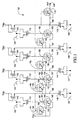
- Fig. 1 is a schematic diagram of a four-stage charge pump 100 of an embodiment of the present invention.
- Charge pump 100 comprises nine triple well NMOS transistors 102-110 and twelve normal NMOS transistors 112-119 and 132-135. These normal NMOS transistors are preferably native n-channel devices that have a low threshold voltage. Normal NMOS transistors 132-135 function as pull up transistors. Normal NMOS transistors 112-119 function as capacitors, and are coupled to clock pulses 122-129. The clock pulses are coupled to the corresponding triple well NMOS transistors via the capacitive action of transistors 112-119. Although there are eight clock pulses, they are arranged in pairs: (122,124), (123,125), (126,128), and (127,129).
- Each clock pulse in a pair has the same pulse timing while different pairs have different pulse timings.
- the clock pulses are shown in Fig. 2 where timings 192-195 correspond to pairs (127,129), (122,125), (126, 128) and (123, 125), respectively. These pulses alternatively boost up the gates of these capacitors. This results in an increase in voltage level from stage to stage.
- the way voltage is being pumped up is similar to a conventional charge pump.
- the output voltage at the drain terminal of triple well NMOS 110 is approximately 10.5 volts while the voltage supplied to charge pump 100 is only 3 volts.
- the use of these triple well transistors enhances the performance and efficiency of charge pump 100 compared to prior art four-stage charge pumps.
- a charge pump preferably includes other associated circuits, e.g., precharge and voltage regulation circuits. These circuits are well known by persons of ordinary skill in the art, and will not be described here.
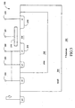
- Fig. 3 shows, schematically, a cross sectional view of a triple well NMOS transistor 200 that can be used for transistors 102-110 of Fig. 1 .
- Transistor 200 is fabricated on a p-type substrate 202.
- An N well 204 is formed in substrate 202, and a P well 206 is formed in N well 204.
- An N+ type drain region 210 is formed in P well 206, as is an N+ source region 212.
- a channel region 214 is defined between source and drain regions in P well 206.
- a polysilicon gate 216 is positioned above channel region 214.
- a thin gate oxide is deposited between gate 216 and channel region 214.
- Drain region 210, gate 216, source region 212, P well 206, and N well 204 are coupled to individual terminals 220-224, respectively.
- triple well transistor 200 can be considered a five-terminal device.
- the N+ source and N+ drain are interchangeable when the charge pump is activated because either terminal may have higher potential than the other.
- the potential of source region 212, P well 206 and N well 204 are set to the same value.
- One way to meet this condition is to electrically connecting terminals 222, 223 and 224.
- the potential of substrate 202 is normally set to ground.
- This arrangement creates a PN diode between P well 206 and drain region 210.
- the diode is inherent in this triple well construction, and does not occupy any extra silicon area. This diode is able to conduct significant amount of current after it is turned on, and thus adds an extra low resistance path to the NMOS transistor. In this application, this diode is called an "extra diode.” As explained in more detail below, this extra diode has the following advantageous effects:
- V T V T ⁇ 0 + ⁇ ⁇ [ V BS + V BI 2 + V BI 2 ]
- V T0 the threshold voltage when there is no substrate bias
- V BS the potential between the source and the body
- V BI the voltage difference of a P-N junction if no external voltage is applied (i.e., zero bias):
- the typical values for V T0 , V BI and ⁇ are 0.7 volt, 0.7 volt, and 0.4, respectively.
- V BS is limited within the P-N junction cut-in voltage of 0.7 volt. This is because when pumping is activated, charge flows from N+ diffusion region 212 to N+ diffusion region 210 through channel 214 and the extra diode created by well 206 and region 210. Thus, the lower potential N+ diffusion region 210, which is the source, suffers minimized substrate bias around 0.7 volt which is much less as compared to more than 10 volts of substrate bias in prior art regulator NMOS charge pumps.
- the charge pump In a charge pump circuit, it is important to generate high forward conduction current so that charges can be build up quickly.
- a low threshold voltage allows the NMOS channels to be turned on faster, and thus can increase the pumping frequency. Because the threshold voltage of the triple well NMOS transistor of the present invention is very low, the pumping frequency of the present inventive charge pump can be much higher than prior art charge pumps. In an embodiment of the present invention, the charge pump can operate efficiently at 22 MHz while prior art charge pump typically operates at 10 MHz.
- Fig. 4 shows a top view 250 of four triple well transistors used in the present invention. It shows two transistors 252 and 254 formed inside a P well 258 and an N well 256. Transistors 252 further comprises a gate 260, a source region 262 and a drain region 264. Transistor 252 could correspond to transistor 102 of Fig. 1 . Transistor 254 further comprises a gate 270, a source region 272 and a drain region 274. Transistor 254 could correspond to transistor 106 of Fig. 1 .
- Fig. 4 also shows two transistor 282 and 284 formed inside a P well 288 and an N well 286.
- Transistor 282 further comprises a gate 290, a source region 292 and a drain region 294.
- Transistor 282 could correspond to transistor 103 of Fig. 1 .
- Transistor 284 further comprises a gate 280, a source region 282 and a drain region 284.
- Transistor 284 could correspond to transistor 107 of Fig. 1 .
- source terminal 141 of transistor 102 and source terminal 142 of transistor 106 are connected to V DD .
- source regions 262 and 272 of transistors 252 and 254, respectively, have the same potential (i.e., V DD ).
- P well 258 and N well 256 should have the same potential as source regions 262 and 272.
- these two wells also have the same potential (V DD ).
- Fig. 1 shows that the gate terminal 144 of transistor 102 is connected to the drain terminal 145 of transistor 106, the source terminal 146 of transistor 103 and the source terminal 147 of transistor 107.
- P well 288 and N well 286 should have the same potential as source regions 292 and 302 (which are coupled to source terminals 146 and 147).
- gate 260, drain region 274, source regions 292 and 302, N well 286 and P well 288 all have the same potential.
- Fig. 1 shows that the drain terminal 150 of transistor 102 is connected to the gate 151 of transistor 106.
- drain region 264 has the same potential as gate 270.
- Fig. 1 shows that the gate terminal 153 of transistor 103 is connected to the drain terminal 154 of transistor 107 (in addition to the source terminals 155 and 156 of transistors 104 and 108).
- gate 290 has the same potential as drain region 304.
- Fig. 1 also shows that the drain terminal 158 of transistor 103 is connected to the gate 159 of transistor 107.
- drain region 294 has the same potential as gate 300.
- Fig. 4 only four of the nine triple well NMOS transistors comprising a charge pump are shown.
- the structure of transistors 104-105 and 108-109 is similar to that shown in Fig. 4 .
- the structure of transistor 110 is similar to that of transistor 254 of Fig. 4 .
- the channel lengths of all the triple well transistors are 1.2 ⁇ m.
- the channel width of transistors 252 and 282 (corresponding to transistors 102 and 103 of Fig. 1 ) is 6 ⁇ m while the channel widths of transistors 254 and 284 (corresponding to transistors 106 and 107 of Fig. 1 ) are 18 ⁇ m.
- Transistors 104 and 105 have the same structure as transistors 102 and 103, respectively. Thus, these two transistors also have a channel length of 1.2 ⁇ m and a channel width of 6 ⁇ m.
- Transistors 108 and 109 have the same structure as transistors 106 and 107, respectively. Thus, these two transistors also have a channel length of 1.2 ⁇ m and a channel width of 18 ⁇ m.
- the channel widths are 15 ⁇ m.
- each table the two right hand columns correspond to the load line of a charge pump constructed using the preferred triple well transistor of the present invention.
- the two columns to the left of these two right hand columns correspond to the load line of the same charge pump constructed using normal transistors. It is observed that the inventive charge pump has a higher current at almost all voltage levels.
- Fig. 5A-5C show voltage profiles at nodes 161-168 and 138 of Fig. 1 .
- Fig. 5A shows four clock pulses which are the same as pulses 124, 125, 128 and 129 of Fig. 2 . These clock pulses are shown here again so as to provide a reference to understand the voltage profiles.
- Fig. 5B shows the voltage profiles 361-365 at nodes 165-168 and 138, respectively.
- Fig. 5C shows the voltage profiles 366-369 at nodes 161-164, respectively. It can be seen at regions 371-373 of Fig. 5B that charges are being pumped to subsequent stages when the triple well transistors 107-109 are turned on.
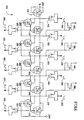
- Fig. 6 is a schematic diagram of a negative charge pump 500 in accordance with the present invention.
- Charge pump 500 comprises eleven triple well NMOS transistors 502-512 and ten P-channel transistors 522-531. These P-channel transistors function as capacitors, and are coupled to clock pulses 534-543. The clock pulses are coupled to the corresponding triple well NMOS transistors via the capacitive action of transistors 522-531.
- Four P-channel transistors 550-553 can be optionally connected to the drain terminals of triple well transistors 508-511 for initial pull-down purpose.
- the output voltage at the source terminal of triple well NMOS 512 is approximately -8 volts when the voltage supplied to charge pump 500 is approximately 3 volts.
- the use of a triple well structure in transistors 502-512 suppresses the body effect and introduces an extra diode in the same way as discussed above in connection with charge pump 100. Thus, all the beneficial effects described above is also present in charge pump 500.
Landscapes
- Engineering & Computer Science (AREA)
- Power Engineering (AREA)
- Dc-Dc Converters (AREA)
- Semiconductor Integrated Circuits (AREA)
Claims (13)
- Pompe à charge comprenant :un corps semiconducteur (202) ayant un type de conductivité particulier,un premier puits (206) dans ledit corps semiconducteur ayant ledit type de conductivité particulier,un deuxième puits (204) dans ledit corps semiconducteur entourant ledit premier puits et ayant un type de conductivité opposé par rapport au type de conductivité particulier,une pluralité de transistors (106 à 110 ; 507 à 512), chacun des transistors dans la pluralité ayant une borne de source et une borne de drain, la pluralité de transistors étant disposés en série d'un premier transistor dans la série relié à une tension d'alimentation (VDD ; GND) à un dernier transistor (110 ; 512) dans la pluralité relié à une sortie de la pompe à charge, pour pomper un niveau de tension de ladite sortie de la pompe à charge en réponse à une ou plusieurs impulsions d'horloge, ledit dernier transistor présentant un niveau de tension sensiblement supérieur à ladite tension d'alimentation pour une sortie de tension positive, ou négative par rapport à celle-ci, pour une sortie de tension négative, la pluralité de transistors dans la série étant connectés de sorte que, pour une sortie de tension positive, la source de l'un des transistors dans la série est connectée au drain d'un transistor précédent dans la série, et pour une sortie de tension négative, le drain de l'un des transistors dans la série est connecté à la source d'un transistor précédent dans la série,caractérisée en ce que
ladite borne de source et ladite borne de drain dudit au moins un transistor de ladite pluralité de transistors comprennent des régions respectives dudit type de conduction opposé formées dans ledit premier puits, ledit premier puits, ledit deuxième puits et ladite région de source étant connectés ensemble. - Pompe à charge selon la revendication 1, dans laquelle ladite tension d'alimentation se trouve dans une plage entre approximativement 5 et approximativement 1,5 volts.
- Pompe à charge selon la revendication 1, dans laquelle ladite tension d'alimentation est sensiblement égale à 3 volts.
- Pompe à charge selon la revendication 1, dans laquelle ladite tension d'alimentation est sensiblement égale à 2 volts.
- Pompe à charge selon la revendication 1, dans laquelle au moins l'une desdites impulsions d'horloge agit à une fréquence au-dessus de 10 MHz.
- Pompe à charge selon la revendication 1, dans laquelle au moins l'une desdites impulsions d'horloge agit à une fréquence approximativement égale à 22 MHz.
- Pompe à charge selon la revendication 1, dans laquelle ledit niveau de tension au niveau dudit dernier transistor est positif.
- Pompe à charge selon la revendication 1, dans laquelle ledit niveau de tension au niveau dudit dernier transistor est négatif.
- Pompe à charge selon la revendication 1, comprenant en outre un moyen destiné à coupler lesdites impulsions d'horloge auxdits transistors.
- Pompe à charge selon la revendication 12, dans laquelle ledit moyen de couplage comprend un transistor MOS.
- Pompe à charge selon la revendication 1, dans laquelle ladite pluralité de transistors comprend une pluralité d'étages de pompe à charge disposés en série pour pomper ledit niveau de tension d'un premier étage à un dernier étage en réponse à ladite une ou plusieurs impulsions d'horloge, et dans laquelle
au moins l'un des étages de la pompe à charge comprend un premier transistor comportant une grille, une source et un drain et un deuxième transistor ayant une grille couplée au drain du premier transistor, une source couplée à la source du premier transistor et un drain couplé à la grille du premier transistor, et dans laquelle les drains et les sources respectifs des premier et deuxième transistors se trouvent dans le premier puits, et les sources des premier et deuxième transistors sont couplées au premier puits. - Pompe à charge selon la revendication 11, dans laquelle le premier puits et le deuxième puits sont couplés ensemble aux sources des premier et deuxième transistors.
- Pompe à charge selon la revendication 1, dans laquelle ladite pluralité de transistors comprend une pluralité d'étages de pompe à charge disposés en série pour pomper ledit niveau de tension d'un premier étage à un dernier étage en réponse auxdites une ou plusieurs impulsions d'horloge, et dans laquelle
l'étage de pompe à charge respectif dans la pluralité comprend un premier puits dans ledit corps semiconducteur ayant ledit type de conductivité particulier, un deuxième puits dans ledit corps semiconducteur entourant ledit premier puits et ayant un type de conductivité opposé par rapport au type de conductivité particulier, un premier transistor comportant une grille, une source et un drain et un deuxième transistor ayant une grille couplée au drain du premier transistor, une source couplée à la source du premier transistor, et un drain couplé à la grille du premier transistor, et dans laquelle les drains et les sources respectifs des premier et deuxième transistors se trouvent dans le premier puits, et les sources des premier et deuxième transistors sont couplées au premier puits.
Applications Claiming Priority (1)
| Application Number | Priority Date | Filing Date | Title |
|---|---|---|---|
| PCT/US1996/016317 WO1998016010A1 (fr) | 1996-10-10 | 1996-10-10 | Pompe a charge avec trois puits |
Publications (3)
| Publication Number | Publication Date |
|---|---|
| EP0931379A1 EP0931379A1 (fr) | 1999-07-28 |
| EP0931379A4 EP0931379A4 (fr) | 2000-01-19 |
| EP0931379B1 true EP0931379B1 (fr) | 2008-08-06 |
Family
ID=22255942
Family Applications (1)
| Application Number | Title | Priority Date | Filing Date |
|---|---|---|---|
| EP96939448A Expired - Lifetime EP0931379B1 (fr) | 1996-10-10 | 1996-10-10 | Pompe a charge avec trois puits |
Country Status (4)
| Country | Link |
|---|---|
| EP (1) | EP0931379B1 (fr) |
| JP (1) | JP3415854B2 (fr) |
| DE (1) | DE69637632D1 (fr) |
| WO (1) | WO1998016010A1 (fr) |
Families Citing this family (7)
| Publication number | Priority date | Publication date | Assignee | Title |
|---|---|---|---|---|
| DE19601369C1 (de) | 1996-01-16 | 1997-04-10 | Siemens Ag | Vorrichtung zur Spannungsvervielfachung, insb. verwendbar zur Erzeugung der Löschspannung für ein EEPROM |
| EP0986166B1 (fr) * | 1998-09-10 | 2010-03-31 | Infineon Technologies AG | Circuit de pompe de charge |
| US6160440A (en) * | 1998-09-25 | 2000-12-12 | Intel Corporation | Scaleable charge pump for use with a low voltage power supply |
| US6441442B1 (en) | 2000-05-30 | 2002-08-27 | Programmable Silicon Solutions | Integrated inductive circuits |
| US6917095B1 (en) | 2000-05-30 | 2005-07-12 | Altera Corporation | Integrated radio frequency circuits |
| EP1160842A3 (fr) * | 2000-05-30 | 2003-09-17 | Programmable Silicon Solutions | Circuits integrés à haute fréquence |
| WO2001093317A1 (fr) * | 2000-05-30 | 2001-12-06 | Programmable Silicon Solutions | Circuits inducteurs integres |
Family Cites Families (5)
| Publication number | Priority date | Publication date | Assignee | Title |
|---|---|---|---|---|
| NL8702734A (nl) * | 1987-11-17 | 1989-06-16 | Philips Nv | Spanningsvermenigvuldigschakeling en gelijkrichtelement. |
| JP2771729B2 (ja) * | 1992-04-16 | 1998-07-02 | 三菱電機株式会社 | チャージポンプ回路 |
| JP3307453B2 (ja) * | 1993-03-18 | 2002-07-24 | ソニー株式会社 | 昇圧回路 |
| JP3282915B2 (ja) * | 1994-03-31 | 2002-05-20 | 富士通株式会社 | Dc/dcコンバータ及びnmosトランジスタのバックゲート電圧の制御方法 |
| TW271011B (fr) * | 1994-04-20 | 1996-02-21 | Nippon Steel Corp |
-
1996
- 1996-10-10 WO PCT/US1996/016317 patent/WO1998016010A1/fr not_active Ceased
- 1996-10-10 JP JP51747498A patent/JP3415854B2/ja not_active Expired - Lifetime
- 1996-10-10 DE DE69637632T patent/DE69637632D1/de not_active Expired - Lifetime
- 1996-10-10 EP EP96939448A patent/EP0931379B1/fr not_active Expired - Lifetime
Also Published As
| Publication number | Publication date |
|---|---|
| WO1998016010A1 (fr) | 1998-04-16 |
| DE69637632D1 (de) | 2008-09-18 |
| HK1021268A1 (en) | 2000-06-02 |
| EP0931379A1 (fr) | 1999-07-28 |
| EP0931379A4 (fr) | 2000-01-19 |
| JP3415854B2 (ja) | 2003-06-09 |
Similar Documents
| Publication | Publication Date | Title |
|---|---|---|
| US6100557A (en) | Triple well charge pump | |
| US7102422B1 (en) | Semiconductor booster circuit having cascaded MOS transistors | |
| US6914791B1 (en) | High efficiency triple well charge pump circuit | |
| US6747897B2 (en) | Semiconductor charge pump circuit and nonvolatile semiconductor memory device | |
| US6878981B2 (en) | Triple-well charge pump stage with no threshold voltage back-bias effect | |
| KR910007403B1 (ko) | 반도체 집적회로 | |
| KR100270926B1 (ko) | 승압회로 | |
| KR100367316B1 (ko) | 승압된백게이트바이어스를갖는승압회로 | |
| JP4026947B2 (ja) | 昇圧回路 | |
| JPH0845291A (ja) | 単一低電圧電源を用いてフローティングゲートメモリセルをプログラムする方法および回路 | |
| US5581107A (en) | Nonvolatile semiconductor memory that eases the dielectric strength requirements | |
| US7439795B2 (en) | Charge pump circuit with reduced parasitic capacitance | |
| EP0843402A1 (fr) | Pompe de charge négative avec BICMOS | |
| US9536575B2 (en) | Power source for memory circuitry | |
| JPH07154964A (ja) | 低電圧チャージポンプ | |
| EP0931379B1 (fr) | Pompe a charge avec trois puits | |
| US5723985A (en) | Clocked high voltage switch | |
| EP0772200A1 (fr) | Générateur de tension pour cellules de mémoire morte programmable électriquement | |
| JP2000503840A (ja) | 三重ウエルの電荷ポンプ | |
| WO1997018588A1 (fr) | Pompes a charge ameliorees utilisant des condensateurs a accumulation | |
| HK1021268B (en) | Triple well charge pump | |
| US6774707B1 (en) | Charge pump circuits and methods | |
| JP3354713B2 (ja) | 半導体昇圧回路 | |
| KR100280456B1 (ko) | 반도체 차지 펌프 회로 | |
| JP3569354B2 (ja) | 半導体昇圧回路 |
Legal Events
| Date | Code | Title | Description |
|---|---|---|---|
| PUAI | Public reference made under article 153(3) epc to a published international application that has entered the european phase |
Free format text: ORIGINAL CODE: 0009012 |
|
| 17P | Request for examination filed |
Effective date: 19990414 |
|
| AK | Designated contracting states |
Kind code of ref document: A1 Designated state(s): DE FR GB IT |
|
| A4 | Supplementary search report drawn up and despatched |
Effective date: 19991202 |
|
| AK | Designated contracting states |
Kind code of ref document: A4 Designated state(s): DE FR GB IT |
|
| RIC1 | Information provided on ipc code assigned before grant |
Free format text: 7H 03K 17/56 A, 7H 03K 17/687 B, 7H 03K 17/74 B, 7H 01L 29/788 B, 7H 02M 3/07 B |
|
| RAP1 | Party data changed (applicant data changed or rights of an application transferred) |
Owner name: MACRONIX INTERNATIONAL CO., LTD. |
|
| 17Q | First examination report despatched |
Effective date: 20020722 |
|
| GRAP | Despatch of communication of intention to grant a patent |
Free format text: ORIGINAL CODE: EPIDOSNIGR1 |
|
| GRAS | Grant fee paid |
Free format text: ORIGINAL CODE: EPIDOSNIGR3 |
|
| GRAA | (expected) grant |
Free format text: ORIGINAL CODE: 0009210 |
|
| AK | Designated contracting states |
Kind code of ref document: B1 Designated state(s): DE FR GB IT |
|
| REG | Reference to a national code |
Ref country code: GB Ref legal event code: FG4D |
|
| REF | Corresponds to: |
Ref document number: 69637632 Country of ref document: DE Date of ref document: 20080918 Kind code of ref document: P |
|
| REG | Reference to a national code |
Ref country code: HK Ref legal event code: GR Ref document number: 1021268 Country of ref document: HK |
|
| PLBE | No opposition filed within time limit |
Free format text: ORIGINAL CODE: 0009261 |
|
| STAA | Information on the status of an ep patent application or granted ep patent |
Free format text: STATUS: NO OPPOSITION FILED WITHIN TIME LIMIT |
|
| 26N | No opposition filed |
Effective date: 20090507 |
|
| REG | Reference to a national code |
Ref country code: DE Ref legal event code: R039 Ref document number: 69637632 Country of ref document: DE Ref country code: DE Ref legal event code: R008 Ref document number: 69637632 Country of ref document: DE |
|
| REG | Reference to a national code |
Ref country code: DE Ref legal event code: R097 Ref document number: 69637632 Country of ref document: DE Ref country code: DE Ref legal event code: R040 Ref document number: 69637632 Country of ref document: DE |
|
| REG | Reference to a national code |
Ref country code: DE Ref legal event code: R082 Ref document number: 69637632 Country of ref document: DE Representative=s name: WALLINGER RICKER SCHLOTTER TOSTMANN PATENT- UN, DE |
|
| REG | Reference to a national code |
Ref country code: DE Ref legal event code: R039 Ref document number: 69637632 Country of ref document: DE Effective date: 20141110 |
|
| REG | Reference to a national code |
Ref country code: DE Ref legal event code: R040 Ref document number: 69637632 Country of ref document: DE Effective date: 20150127 |
|
| REG | Reference to a national code |
Ref country code: FR Ref legal event code: PLFP Year of fee payment: 20 |
|
| PGFP | Annual fee paid to national office [announced via postgrant information from national office to epo] |
Ref country code: FR Payment date: 20150908 Year of fee payment: 20 |
|
| PGFP | Annual fee paid to national office [announced via postgrant information from national office to epo] |
Ref country code: GB Payment date: 20151007 Year of fee payment: 20 Ref country code: IT Payment date: 20151026 Year of fee payment: 20 Ref country code: DE Payment date: 20151006 Year of fee payment: 20 |
|
| REG | Reference to a national code |
Ref country code: DE Ref legal event code: R071 Ref document number: 69637632 Country of ref document: DE |
|
| REG | Reference to a national code |
Ref country code: GB Ref legal event code: PE20 Expiry date: 20161009 |
|
| PG25 | Lapsed in a contracting state [announced via postgrant information from national office to epo] |
Ref country code: GB Free format text: LAPSE BECAUSE OF EXPIRATION OF PROTECTION Effective date: 20161009 |