EP0931380B1 - Rekonfigurierbares rechnersystem - Google Patents
Rekonfigurierbares rechnersystem Download PDFInfo
- Publication number
- EP0931380B1 EP0931380B1 EP97933815A EP97933815A EP0931380B1 EP 0931380 B1 EP0931380 B1 EP 0931380B1 EP 97933815 A EP97933815 A EP 97933815A EP 97933815 A EP97933815 A EP 97933815A EP 0931380 B1 EP0931380 B1 EP 0931380B1
- Authority
- EP
- European Patent Office
- Prior art keywords
- dram
- configuration
- array
- bit
- row
- Prior art date
- Legal status (The legal status is an assumption and is not a legal conclusion. Google has not performed a legal analysis and makes no representation as to the accuracy of the status listed.)
- Expired - Lifetime
Links
Images


Classifications
-
- G—PHYSICS
- G06—COMPUTING OR CALCULATING; COUNTING
- G06F—ELECTRIC DIGITAL DATA PROCESSING
- G06F15/00—Digital computers in general; Data processing equipment in general
- G06F15/76—Architectures of general purpose stored program computers
- G06F15/78—Architectures of general purpose stored program computers comprising a single central processing unit
- G06F15/7867—Architectures of general purpose stored program computers comprising a single central processing unit with reconfigurable architecture
-
- H—ELECTRICITY
- H03—ELECTRONIC CIRCUITRY
- H03K—PULSE TECHNIQUE
- H03K19/00—Logic circuits, i.e. having at least two inputs acting on one output; Inverting circuits
- H03K19/02—Logic circuits, i.e. having at least two inputs acting on one output; Inverting circuits using specified components
- H03K19/173—Logic circuits, i.e. having at least two inputs acting on one output; Inverting circuits using specified components using elementary logic circuits as components
- H03K19/177—Logic circuits, i.e. having at least two inputs acting on one output; Inverting circuits using specified components using elementary logic circuits as components arranged in matrix form
Definitions
- the present invention relates to reconfigurable computing, being more particularly, though not exclusively concerned with field programmable gate array (FPGA) and similar architectures.
- FPGA field programmable gate array
- Reconfigurable gate arrays also known as field programmable gate arrays (FPGA) are widely used in the industry to implement a variety of digital circuits.
- the application areas include computers, workstations, control systems, etc.
- a typical traditional FPGA device contains a number of logic cells which are configured to meet the specific design requirements.
- An unprogrammed FPGA contains a predefined logic cell structure as later described. Each of these said cells is configured to perform a specific task (a logical circuit) to achieve the desired functionality.
- the programming information is generally loaded serially into the FPGA as a relatively slow process (some devices are loaded via 8 bits wide bus, still a very slow process), where it is retained internally so long as power is applied to the device, by the configuration storage elements typically implemented as distributed static RAM (SRAM).
- SRAM distributed static RAM
- the device can also be reconfigured while the power is on by following a predefined programming sequence which includes the before-described slow serial loading of the reconfiguration data.
- a predefined programming sequence which includes the before-described slow serial loading of the reconfiguration data.
- Xilinx Corporation's device XC4025 a traditional FPGA, requires 422,128 bits of programming information and takes nearly 42ms to completely program (or reconfigure) the device. As the device size gets larger, this delay gets bigger.
- the invention is designed to eliminate current reconfiguration limitations and related problems and provide significantly enhanced system performance and at reduced cost, enabling substantially universal usage for many applications as a result of providing on-the-fly alterable chip or other logic architecture.
- a big digital integrated circuit design is simulated prior to its expensive and time consuming fabrication cycle to maximize its chances of correct functioning after fabrication.
- the design is extensively checked on high performance engineering workstations against all possible input conditions by providing stimulus and observing the response. If the response does not meet the expected results, the design is checked for correctness. This iterative process is continued until all possible scenarios have been verified. Simulation is extremely time consuming, expensive and increases the time to market, but this problem is a critical part of the design methodology and is currently managed by splitting the large simulation tasks among a number of engineers and then compiling the results -- a very error prone process, though it does speed up the task at substantially higher cost.
- An objective of the invention accordingly, is to provide a new and improved dynamically reconfigurable gate array system, architecture and method utilizing a novel DRAM-based configuration control structure that obviates current reconfigurability limitations including those above described, and related problems, while providing significantly enhanced system performance at low cost, and which thereby enable substantially universal usage for myriads of applications.
- Another object is to provide a method and apparatus to self modify the logic implementation based on pre-determined criteria.
- a further object is to provide such a novel system in which a large amount of memory is available internal to the FPGA and is accessed with a small number of pins, such that the reconfiguration time is 4 orders of magnitude faster than the traditional approaches, and at notably low cost.
- Still another object is to provide a system based on this novel architecture that works equally efficiently in both non-reconfiguration and reconfiguration applications.
- the invention enhances a method of configuring an array of programmable logic cells each having logic functions controlled by an associated configuration bit memory, that comprises the steps of storing bit information defining multiple program configurations in a DRAM core; connecting a bus to the array to enable a DRAM row wide loading of the configuration bit memories of the cells with bit information defining a desired configuration; and, upon a configuration command, retrieving from the DRAM core, at least a row at a time, the configuration bit information, and loading such information in the bit memories of the cells to control the corresponding cell logic functions to achieve the desired configuration programming.
- the invention also concerns a corresponding apparatus as defined in claim 10.
- Fig. 1 shows the prior art FPGA interface using FPGA units (#1 - -- #n) programmed through a bus system, so-labelled, by a CPU working with main memory.
- the FPGA units have the internal logic cell structure or array and routing channels of Fig. 2, with each configurable logic cell having logic functions controlled by an associated configuration static RAM (SRAM) as represented in Fig. 3, wherein the configuration data is stored in the small localized internal static RAM bits.
- SRAM configuration static RAM
- a DRAM core as shown in Fig. 4, is used to store multiple configurations.
- the configuration SRAM bits required for the device configuration are also provided.
- a DRAM row wide bus is provided (where the term "row” as used herein also embraces a part or fraction of a row), which connects directly to the SRAM bits, which then subsequently control the programmable elements. After a configuration command is given, a row is retrieved each time and is stored in the said SRAM bits, until all the necessary configuration storage elements have been loaded. A partial reconfiguration is achieved by only loading those SRAM bits which need be changed.
- a further enhancement of this invention is to provide masking capability such that only bits which need be changed are allowed to be loaded into configuration SRAM. It is also possible to load new configuration data into the DRAM while the chip is operational.
- the same DRAM is also usable as storage space accessible from both the external I/O or via the internal logic.
- the bus does not have to be a full row wide and can be a fraction of row still herein termed a "row" as before stated, with corresponding reduction in performance.
- An alternate embodiment of this invention involves using two identical banks of DRAMs such that the identical configuration data is loaded in both of them. Assuming that a row provides sufficient data to configure the entire FPGA, then no SRAM bits are required; and when one bank is being refreshed, another one provides the configuration data. The concept can be extended to 'm' banks such that 'm/2' banks have the same configuration information as the other 'm/2' banks.
- a serial stream of multiplexed data can be split among its constituent serial streams, converted to parallel format and simultaneously loaded into a DRAM row at different predetermined column addresses.
- an internal DRAM bank is used for reconfiguration data only while another internal bank is primarily used for general purpose memory, such that externally both banks are accessed via the same interface to minimize the cost.
- a self-modifying circuit can be designed with one possible implementation shown in Fig. 5.
- a small SRAM core with data width equal to the number of bits required to decode each row address uniquely, drives the selected row addresses of the DRAM. internally.
- the number of SRAM core address locations in this self-modifying architecture is subject to the required depth of the reconfiguration capability. As an example, in this case, it is shown as 32 x 9 SRAM.
- the output of the SRAM core is used to retrieve the row wide configuration data.
- the new circuit implementation may have different control logic driving the SRAM core address inputs, subject to the state of various circuit elements, resulting in yet another circuit functionality implementation; and so on and so forth, automatically.
- the chip functionality can be dynamically altered to a predetermined logic implementation subject to the outcome of certain logic conditions.
- This technique provides a highly efficient self-modifying circuit requiring minimum intervention from the associated CPU, thus enhancing the overall system performance significantly, and has wide ranging applications in digital signal processing algorithms, pipelined designs etc.
- One potential application is to segment a large pipelined design into multiple configurations and these configurations are loaded as required by the processing hardware. This significantly reduces the number of gates required to implement designs due to reusability of the gates, thereby reducing the chip cost. This is only achievable because of the very high speed "on-the-fly" self-modifying capability.
- the SRAM core can also be implemented with other technologies such as Flash or EEPROM.
- 'JAVA' the most widely used Internet language
- 'JAVA' which is specifically designed to be platform independent, thereby providing complete portability among various machines.
- the disadvantage is that 'JAVA' runs extremely slow as it does not take advantage of unique architectural capabilities of different CPUs.
- One approach to improve 'JAVA' execution speed is by providing it a common virtual hardware platform (in addition to the traditional CPU functionality), alterable at very high speed.
- This virtual hardware is implemented either by providing reconfigurability with 'SONAL' capability on CPUs themselves or implemented as a separate 'SONAL' FPGA. This architecture thus retains the key element of platform independence, yet provides higher speed execution.
- the chip has somewhat different pinout to reflect its unique architecture.
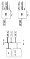
- One possible pinout is shown exemplarily in Fig. 7, providing a traditional DRAM interface with separate address and data buses.
- a 'SONAL' with 256K x 8 DRAM Using the traditional DRAM access approach, 21 pins are required (9 for address, 8 for data, 1 each for 'RAS', 'CAS', 'WRITE' and 'Output Enable').
- a 'WAIT signal is also provided for the system bus interface whenever an internal transfer between the FPGA cells and the DRAM core is taking place.
- the CPU (or other master controller) can either use it to delay the start of access, or in an alternate implementation, the access cycle can be extended to allow for the internal transfer to complete, before proceeding with this access.
- 'PARAS' DRAM interface access mechanism of said copending application
- This application discloses a method of and apparatus for improving the accessing capability of asynchronous and synchronous dynamic random access memory devices by a novel interfacing and accessing procedure in which the same pins are used for each of row, column and data accessing and in both the read and write cycles; such enabling effectively increasing the data bandwidth and addressing range in substantially the same size packages but with fewer pins.
- 'PARAS' model only 13 pins and one additional for 'WAIT are needed as shown in Fig. 8. It should be noted, furthermore, that in applications where it is not necessary to access the DRAM after the configuration data has been loaded, and, hence no external access is required, the same pins can be used as traditional FPGA I/O pins.
- the adder simulation typically will take a few clock cycles.
- the 'SONAL' can be dynamically reconfigured and then the function can be verified by executing the task in real time on such configured 'SONAL'. This compares well against the traditional workstation without 'SONAL' approach, which typically takes thousands of cycles.
Landscapes
- Engineering & Computer Science (AREA)
- Computer Hardware Design (AREA)
- Theoretical Computer Science (AREA)
- Physics & Mathematics (AREA)
- General Engineering & Computer Science (AREA)
- General Physics & Mathematics (AREA)
- Mathematical Physics (AREA)
- Computing Systems (AREA)
- Logic Circuits (AREA)
- Dram (AREA)
- Hardware Redundancy (AREA)
- Debugging And Monitoring (AREA)
- Electrotherapy Devices (AREA)
Claims (26)
- Verfahren zum Konfigurieren eines Feldes von programmierbaren logischen Zellen, deren jede logische Funktionen hat, die durch einen zugeordneten Konfigurations-Bit-Speicher gesteuert werden, dadurch gekennzeichnet, dass Bit-Informationen gespeichert werden, die Mehrfach-Programm-Konfigurationen in einem DRAM-Kern definieren, dass ein Bus mit dem Feld verbunden wird, damit ein DRAM in die Lage versetzt wird, in Reihenbreite die Konfigurations-Bit-Speicher der Zellen mit Bit-Informationen zu laden, die eine gewünschte Konfiguration definieren, und dass bei einem Konfigurationsbefehl die Konfigurations-Bit-Informationen aus dem DRAM-Kern mit mindestens einer Reihe gleichzeitig wieder aufgefunden werden und diese Informationen in die Bit-Speicher der Zellen geladen werden, um die entsprechenden Funktionen der logischen Zellenfunktionen zu steuern, damit die gewünschte Konfigurations-Programmierung erreicht wird.
- Verfahren nach Anspruch 1, bei dem durch das Wiederauffinden einer Reihe gleichzeitig und das Laden eine erneute Konfiguration fliegend vorgenommen werden kann.
- Verfahren nach Anspruch 1, bei dem das Feld eine FPGA-Vorrichtung aufweist und die logischen Zellen-Bit-Speicher SRAM-verteilte Bits aufweisen.
- Verfahren nach Anspruch 1, bei dem bei Beendigung einer Funktion durch das Feld von logischen Zellen ein Bit-Befehl erzeugt wird, der eine neue gewünschte Funktionalität des Feldes anzeigt, und ein zusätzlicher Speicherkern vorgesehen ist, der die Bit-Adresse einer DRAM-Reihe enthält und so geschaltet ist, dass er auf den nächsten Funktionalitäts-Bit-Befehl anspricht und entsprechend den DRAM antreibt, wobei die Konfigurations-Bit-Informationrn, die die nächste Funktionalität darstellen, wieder aufgefunden und in die Bit-Speicher der Zellen geladen werden, indem die entsprechenden logischen Zellenfunktionen gesteuert werden und damit das Feld sich selbst rekonfiguriert, um die nächste Funktionalität auszuführen.
- Verfahren nach Anspruch 4, bei dem die Selbst-Rekonfiguralität sich in nachfolgende gewünschte Funktionalitäts-Befehle fortsetzt.
- Verfahren nach Anspruch 3, bei dem eine teilweise Rekonfiguration durch Laden nur der SRAM-Bits durchgeführt wird, die geändert werden sollen.
- Verfahren nach Anspruch 1, bei dem der DRAM-Kern ferner als Speicherraum verwendet wird, der sowohl von der externen I/O Schnittstelle als auch der internen Logik zugreifbar ist.
- Verfahren nach Anspruch 7, bei dem während der externen Verbindung der interne reihenweite Bus ein Maximum an reihenweiten Daten in einen Zugriff speichert/wiederauffindet, und, wenn eine Reihe intern ausgewählt worden ist, rasch Spaltendaten zugreift.
- Verfahren nach Anspruch 1, bei dem neue Konfigurationsdaten in den DRAM-Kern während des Betriebes der Vorrichtung geladen werden.
- Einrichtung zum Konfigurieren eines Feldes von programmierbaren logischen Zellen, deren jede logische Funktionen hat, die durch einen zugeordneten Konfigurations-Bit-Speicher gesteuert werden, gekennzeichnet durch die Kombination folgender Merkmale: Einen DRAM-Speicher zum Speichern von Bit-Informationen, die Mehrfach-Programm-Konfigurationen definieren, einen Bus, der das Feld und den DRAM-Kern so miteinander verbindet, dass ein DRAM in die Lage versetzt wird, reihenweit die Konfigurations-Bit-Speicher des Feldes von logischen Zellen mit Bit-Informationen zu laden, die eine gewünschte Konfiguraiton definieren, eine Vorrichtung zum Erzeugen eines Konfigurationsbefehls und bei einem solchen Konfigurationsbefehl und darauf ansprechend eine Vorrichtung zum Wiederauffinden der Konfigurations-Bit-Informationen aus dem DRAM-Kern bei mindestens einer Reihe gleichzeitig, und eine Vorrichtung zum Laden dieser Informationen in die Bit-Speicher der logischen Zellen, um die entsprechenden Funktionen der logischen Zellen zu steuern und damit die gewünschte Konfiguations-Programmierung zu erzielen.
- Einrichtung nach Anspruch 10, bei der das Feld eine FPGA-Vorrichtung und die Bit-Speicher der logischen Zelle SRAM-verteilte Bits aufweisen.
- Einrichtung nach Anspruch 10, bei der eine Zugriffs-Steuerschaltung vorgesehen ist, die mit dem Eingang des DRAM-Kernes und mit einem oder beiden eines DRAM-Entscheidungs- und Auffrischungs-Logikmoduls, das auf einen Konfigurations-Befehl anspricht, der intern aus dem Feld von logischen Zellen entsteht, sowie mit einer externen DRAM-Schnittstelle verbunden ist.
- Einrichtung nach Anspruch 11, bei der eine Zugriffs-Steuerschaltung vorgesehen ist, die mit dem Eingang des DRAM-Kernes verbunden ist und auf Daten-Bits anspricht, die einer DRAM-Reihenadresse entspricht, die aus einer SRAM-Speicherkerneinheit entsteht, die eine Datenbreite gleich der Anzahl von Bits enthält, wie sie erforderlich sind, um DRAM-Reihenadressen eindeutig zu decodieren, wodurch die ausgewählten Reihenadressen des DRAM intern betrieben werden, und die SRAM-Einheit so geschaltet ist, dass sie Adressen-Bit-Konfigurations-Befehlssignale aus dem Feld von logischen Zellen aufnimmt.
- Einrichtung nach Anspruch 13, bei der das Konfigurations-Befehlssignal bei Beendigung einer Funktion durch das Feld von logischen Zellen als eine neue Konfiguration für eine nächste gewünschte Funktionalität des Feldes generiert wird und aufgrund der designierten DRAM-Reihenadresse entsprechend der DRAM-Kern aus der Zugriffs-Steuervorrichtung decodiert wird, eine Vorrichtung zum Laden der Konfigurations-Bit-Informationen, die die nächste Funktionalität repräsentieren, wie sie von dem DRAM-Kern zurückgegeben wird, in die Bit-Speicher der logischen Zellen, wodurch die entsprechenden Funktionen der logischen Zellen gesteuert werden, und damit das Feld auf diese Weise selbstkonfiguriert wird, um die nächste Funktionalität durchzuführen, wobei diese Selbstkonfigurierung automatisch für nachfolgende gewünschte Funktionalitäts-Befehle fortgesetzt wird.
- Einrichtung nach Anspruch 14, bei der das Feld aus logischen Zellen fünf Adressen-Bits und die SRAM-Einheit neun Daten-Bits entsprechend einer DRAM-Reihenadresse generiert, wobei die SRAM-Einheit 32 x 9 Bits enthält.
- Einrichtung nach Anspruch 10, bei der das Feld logischer Zellen bei Vervollständigung einer Funktion einen Bit-Befehl erzeugt, um eine nächste gewünschte Funktionalität des Feldes anzuzeigen und ferner ein zusätzlicher Speicherkern vorgesehen ist, der die Bit-Adresse einer DRAM-Reihe enthält und zwischen das Feld und den DRAM-Kern eingeschaltet ist, um auf den nächsten Funktionalitäts-Bit-Befehl anzusprechen und entsprechend den DRAM anzutreiben, damit die Konfigurations-Bit-Informationen, die die nächste Funktionalität in den Bit-Speichern der Zellen des Feldes repräsentieren, die entsprechenden logischen Zellenfunktionen steuern, wodurch eine Selbst-Rekonfiguration des Feldes zur Durchführung der nächsten Funktionalität erreicht wird.
- Einrichtung nach Anspruch 16, bei der der zusätzliche Speicherkern einen SRAM-Kern aufweist.
- Einrichtung nach Anspruch 16, bei der die Selbst-Rekonfiguration automatisch für anschließende Befehle gewünschter Funktionalität fortgesetzt wird.
- Einrichtung nach Anspruch 11, bei der nur eine teilweise Rekonfiguraiton durchgeführt wird, wobei die Ladevorrichtung nur die SRAM-Bits lädt, die geändert werden müssen.
- Einrichtung nach Anspruch 10, bei der der DRAM-Kern ferner als Speicherraum verwendet wird, der sowohl von der externen I/O-Schnittstelle als auch der internen Logik zugreifbar ist.
- Einrichtung nach Anspruch 20, bei der während der externen Verbindung der interne reihenweite Bus ein Maximum von reihenweiten Daten in einem Zugriff speichert/wiederauffindet, und, wenn eine Reihe intern ausgewählt worden ist, eine Vorrichtung zum raschen Zugreifen von Spaltendaten vorgesehen ist.
- Einrichtung nach Anspruch 10, bei der das Feld Teil einer programmierbaren Vorrichtung ist und neue Konfigurations-Daten in den DRAM-Kern geladen werden, während die Vorrichtung in Betrieb ist.
- Einrichtung nach Anspruch 22, bei der die Vorrichtung ein FPGA enthält.
- Einrichtung nach Anspruch 11, bei der das reihenweise Wiederauffinden und Laden eine Rekonfiguration fliegend in Betrieb setzt.
- Einrichtung nach Anspruch 11, bei der zwei identische Gruppen von DRAMs mit identischen Konfigurations-Daten, die in jede Gruppe geladen werden, vorgesehen sind.
- Einrichtung nach Anspruch 24, bei der dann, wenn in einer Gruppe der DRAM-Kern bzw. die DRAM-Kerne wieder aufgefrischt wird bzw. werden, die andere die Konfigurations-Daten liefert.
Applications Claiming Priority (3)
| Application Number | Priority Date | Filing Date | Title |
|---|---|---|---|
| US700966 | 1996-08-21 | ||
| US08/700,966 US5838165A (en) | 1996-08-21 | 1996-08-21 | High performance self modifying on-the-fly alterable logic FPGA, architecture and method |
| PCT/IB1997/000987 WO1998008306A1 (en) | 1996-08-21 | 1997-08-12 | Reconfigurable computing system |
Publications (2)
| Publication Number | Publication Date |
|---|---|
| EP0931380A1 EP0931380A1 (de) | 1999-07-28 |
| EP0931380B1 true EP0931380B1 (de) | 2002-07-03 |
Family
ID=24815539
Family Applications (1)
| Application Number | Title | Priority Date | Filing Date |
|---|---|---|---|
| EP97933815A Expired - Lifetime EP0931380B1 (de) | 1996-08-21 | 1997-08-12 | Rekonfigurierbares rechnersystem |
Country Status (10)
| Country | Link |
|---|---|
| US (1) | US5838165A (de) |
| EP (1) | EP0931380B1 (de) |
| JP (1) | JP3801214B2 (de) |
| KR (1) | KR100458371B1 (de) |
| CN (1) | CN1188948C (de) |
| AT (1) | ATE220263T1 (de) |
| AU (1) | AU3705297A (de) |
| CA (1) | CA2264060C (de) |
| DE (1) | DE69713784T2 (de) |
| WO (1) | WO1998008306A1 (de) |
Families Citing this family (238)
| Publication number | Priority date | Publication date | Assignee | Title |
|---|---|---|---|---|
| US5943242A (en) * | 1995-11-17 | 1999-08-24 | Pact Gmbh | Dynamically reconfigurable data processing system |
| US7266725B2 (en) | 2001-09-03 | 2007-09-04 | Pact Xpp Technologies Ag | Method for debugging reconfigurable architectures |
| DE19651075A1 (de) | 1996-12-09 | 1998-06-10 | Pact Inf Tech Gmbh | Einheit zur Verarbeitung von numerischen und logischen Operationen, zum Einsatz in Prozessoren (CPU's), Mehrrechnersystemen, Datenflußprozessoren (DFP's), digitalen Signal Prozessoren (DSP's) oder dergleichen |
| DE19654595A1 (de) | 1996-12-20 | 1998-07-02 | Pact Inf Tech Gmbh | I0- und Speicherbussystem für DFPs sowie Bausteinen mit zwei- oder mehrdimensionaler programmierbaren Zellstrukturen |
| US6338106B1 (en) | 1996-12-20 | 2002-01-08 | Pact Gmbh | I/O and memory bus system for DFPS and units with two or multi-dimensional programmable cell architectures |
| ATE243390T1 (de) | 1996-12-27 | 2003-07-15 | Pact Inf Tech Gmbh | Verfahren zum selbständigen dynamischen umladen von datenflussprozessoren (dfps) sowie bausteinen mit zwei- oder mehrdimensionalen programmierbaren zellstrukturen (fpgas, dpgas, o.dgl.) |
| DE19654846A1 (de) | 1996-12-27 | 1998-07-09 | Pact Inf Tech Gmbh | Verfahren zum selbständigen dynamischen Umladen von Datenflußprozessoren (DFPs) sowie Bausteinen mit zwei- oder mehrdimensionalen programmierbaren Zellstrukturen (FPGAs, DPGAs, o. dgl.) |
| DE19704728A1 (de) | 1997-02-08 | 1998-08-13 | Pact Inf Tech Gmbh | Verfahren zur Selbstsynchronisation von konfigurierbaren Elementen eines programmierbaren Bausteines |
| US6542998B1 (en) | 1997-02-08 | 2003-04-01 | Pact Gmbh | Method of self-synchronization of configurable elements of a programmable module |
| DE19704742A1 (de) | 1997-02-11 | 1998-09-24 | Pact Inf Tech Gmbh | Internes Bussystem für DFPs, sowie Bausteinen mit zwei- oder mehrdimensionalen programmierbaren Zellstrukturen, zur Bewältigung großer Datenmengen mit hohem Vernetzungsaufwand |
| US6160419A (en) * | 1997-11-03 | 2000-12-12 | Altera Corporation | Programmable logic architecture incorporating a content addressable embedded array block |
| US6011407A (en) * | 1997-06-13 | 2000-01-04 | Xilinx, Inc. | Field programmable gate array with dedicated computer bus interface and method for configuring both |
| US6092123A (en) * | 1997-07-17 | 2000-07-18 | International Business Machines Corporation | Method and apparatus for changing functions of a hardware device using two or more communication channels |
| US8686549B2 (en) | 2001-09-03 | 2014-04-01 | Martin Vorbach | Reconfigurable elements |
| US6034542A (en) * | 1997-10-14 | 2000-03-07 | Xilinx, Inc. | Bus structure for modularized chip with FPGA modules |
| US5923892A (en) * | 1997-10-27 | 1999-07-13 | Levy; Paul S. | Host processor and coprocessor arrangement for processing platform-independent code |
| DE19861088A1 (de) | 1997-12-22 | 2000-02-10 | Pact Inf Tech Gmbh | Verfahren zur Reparatur von integrierten Schaltkreisen |
| US6034538A (en) * | 1998-01-21 | 2000-03-07 | Lucent Technologies Inc. | Virtual logic system for reconfigurable hardware |
| DE19807872A1 (de) | 1998-02-25 | 1999-08-26 | Pact Inf Tech Gmbh | Verfahren zur Verwaltung von Konfigurationsdaten in Datenflußprozessoren sowie Bausteinen mit zwei- oder mehrdimensionalen programmierbaren Zellstruktur (FPGAs, DPGAs, o. dgl. |
| US7146441B1 (en) * | 1998-03-16 | 2006-12-05 | Actel Corporation | SRAM bus architecture and interconnect to an FPGA |
| US6038627A (en) * | 1998-03-16 | 2000-03-14 | Actel Corporation | SRAM bus architecture and interconnect to an FPGA |
| US6430732B1 (en) | 1998-03-27 | 2002-08-06 | Xilinx, Inc. | Method for structured layout in a hardware description language |
| US6216258B1 (en) | 1998-03-27 | 2001-04-10 | Xilinx, Inc. | FPGA modules parameterized by expressions |
| US6243851B1 (en) | 1998-03-27 | 2001-06-05 | Xilinx, Inc. | Heterogeneous method for determining module placement in FPGAs |
| US6292925B1 (en) | 1998-03-27 | 2001-09-18 | Xilinx, Inc. | Context-sensitive self implementing modules |
| US6237129B1 (en) | 1998-03-27 | 2001-05-22 | Xilinx, Inc. | Method for constraining circuit element positions in structured layouts |
| US6260182B1 (en) * | 1998-03-27 | 2001-07-10 | Xilinx, Inc. | Method for specifying routing in a logic module by direct module communication |
| US6826749B2 (en) | 1998-12-08 | 2004-11-30 | Nazomi Communications, Inc. | Java hardware accelerator using thread manager |
| US7225436B1 (en) | 1998-12-08 | 2007-05-29 | Nazomi Communications Inc. | Java hardware accelerator using microcode engine |
| US20050149694A1 (en) * | 1998-12-08 | 2005-07-07 | Mukesh Patel | Java hardware accelerator using microcode engine |
| US6332215B1 (en) | 1998-12-08 | 2001-12-18 | Nazomi Communications, Inc. | Java virtual machine hardware for RISC and CISC processors |
| US6081473A (en) * | 1998-12-15 | 2000-06-27 | Lattice Semiconductor Corporation | FPGA integrated circuit having embedded sram memory blocks each with statically and dynamically controllable read mode |
| US7003660B2 (en) * | 2000-06-13 | 2006-02-21 | Pact Xpp Technologies Ag | Pipeline configuration unit protocols and communication |
| US6262596B1 (en) * | 1999-04-05 | 2001-07-17 | Xilinx, Inc. | Configuration bus interface circuit for FPGAS |
| DE10081643D2 (de) | 1999-06-10 | 2002-05-29 | Pact Inf Tech Gmbh | Sequenz-Partitionierung auf Zellstrukturen |
| US6347346B1 (en) * | 1999-06-30 | 2002-02-12 | Chameleon Systems, Inc. | Local memory unit system with global access for use on reconfigurable chips |
| DE19946752A1 (de) * | 1999-09-29 | 2001-04-12 | Infineon Technologies Ag | Rekonfigurierbares Gate-Array |
| US6555398B1 (en) * | 1999-10-22 | 2003-04-29 | Magic Corporation | Software programmable multiple function integrated circuit module |
| US6438737B1 (en) * | 2000-02-15 | 2002-08-20 | Intel Corporation | Reconfigurable logic for a computer |
| DE10018374A1 (de) * | 2000-04-13 | 2001-10-18 | Siemens Ag | Mobiles Endgerät |
| US7119576B1 (en) | 2000-09-18 | 2006-10-10 | Altera Corporation | Devices and methods with programmable logic and digital signal processing regions |
| US7346644B1 (en) | 2000-09-18 | 2008-03-18 | Altera Corporation | Devices and methods with programmable logic and digital signal processing regions |
| US8058899B2 (en) | 2000-10-06 | 2011-11-15 | Martin Vorbach | Logic cell array and bus system |
| AU2002220600A1 (en) | 2000-10-06 | 2002-04-15 | Pact Informationstechnologie Gmbh | Cell system with segmented intermediate cell structure |
| EP1197847A3 (de) * | 2000-10-10 | 2003-05-21 | Nazomi Communications Inc. | Java-Hardwarebeschleuniger mit Mikrokodemaschine |
| US6990555B2 (en) | 2001-01-09 | 2006-01-24 | Pact Xpp Technologies Ag | Method of hierarchical caching of configuration data having dataflow processors and modules having two- or multidimensional programmable cell structure (FPGAs, DPGAs, etc.) |
| DE10105987A1 (de) * | 2001-02-09 | 2002-08-29 | Infineon Technologies Ag | Datenverarbeitungsvorrichtung |
| US9037807B2 (en) | 2001-03-05 | 2015-05-19 | Pact Xpp Technologies Ag | Processor arrangement on a chip including data processing, memory, and interface elements |
| US7210129B2 (en) | 2001-08-16 | 2007-04-24 | Pact Xpp Technologies Ag | Method for translating programs for reconfigurable architectures |
| US7444531B2 (en) | 2001-03-05 | 2008-10-28 | Pact Xpp Technologies Ag | Methods and devices for treating and processing data |
| US7581076B2 (en) | 2001-03-05 | 2009-08-25 | Pact Xpp Technologies Ag | Methods and devices for treating and/or processing data |
| US7844796B2 (en) | 2001-03-05 | 2010-11-30 | Martin Vorbach | Data processing device and method |
| US7249242B2 (en) | 2002-10-28 | 2007-07-24 | Nvidia Corporation | Input pipeline registers for a node in an adaptive computing engine |
| US7489779B2 (en) | 2001-03-22 | 2009-02-10 | Qstholdings, Llc | Hardware implementation of the secure hash standard |
| US7400668B2 (en) | 2001-03-22 | 2008-07-15 | Qst Holdings, Llc | Method and system for implementing a system acquisition function for use with a communication device |
| US7752419B1 (en) | 2001-03-22 | 2010-07-06 | Qst Holdings, Llc | Method and system for managing hardware resources to implement system functions using an adaptive computing architecture |
| US7653710B2 (en) | 2002-06-25 | 2010-01-26 | Qst Holdings, Llc. | Hardware task manager |
| US6836839B2 (en) | 2001-03-22 | 2004-12-28 | Quicksilver Technology, Inc. | Adaptive integrated circuitry with heterogeneous and reconfigurable matrices of diverse and adaptive computational units having fixed, application specific computational elements |
| US7962716B2 (en) | 2001-03-22 | 2011-06-14 | Qst Holdings, Inc. | Adaptive integrated circuitry with heterogeneous and reconfigurable matrices of diverse and adaptive computational units having fixed, application specific computational elements |
| US6577678B2 (en) | 2001-05-08 | 2003-06-10 | Quicksilver Technology | Method and system for reconfigurable channel coding |
| JP3561506B2 (ja) * | 2001-05-10 | 2004-09-02 | 東京エレクトロンデバイス株式会社 | 演算システム |
| US10031733B2 (en) * | 2001-06-20 | 2018-07-24 | Scientia Sol Mentis Ag | Method for processing data |
| WO2002103532A2 (de) | 2001-06-20 | 2002-12-27 | Pact Xpp Technologies Ag | Verfahren zur bearbeitung von daten |
| US6706402B2 (en) | 2001-07-25 | 2004-03-16 | Nantero, Inc. | Nanotube films and articles |
| US6574130B2 (en) | 2001-07-25 | 2003-06-03 | Nantero, Inc. | Hybrid circuit having nanotube electromechanical memory |
| US6643165B2 (en) | 2001-07-25 | 2003-11-04 | Nantero, Inc. | Electromechanical memory having cell selection circuitry constructed with nanotube technology |
| US6919592B2 (en) | 2001-07-25 | 2005-07-19 | Nantero, Inc. | Electromechanical memory array using nanotube ribbons and method for making same |
| US6835591B2 (en) | 2001-07-25 | 2004-12-28 | Nantero, Inc. | Methods of nanotube films and articles |
| US6924538B2 (en) | 2001-07-25 | 2005-08-02 | Nantero, Inc. | Devices having vertically-disposed nanofabric articles and methods of making the same |
| US6911682B2 (en) | 2001-12-28 | 2005-06-28 | Nantero, Inc. | Electromechanical three-trace junction devices |
| US7566478B2 (en) | 2001-07-25 | 2009-07-28 | Nantero, Inc. | Methods of making carbon nanotube films, layers, fabrics, ribbons, elements and articles |
| US7259410B2 (en) | 2001-07-25 | 2007-08-21 | Nantero, Inc. | Devices having horizontally-disposed nanofabric articles and methods of making the same |
| US7996827B2 (en) | 2001-08-16 | 2011-08-09 | Martin Vorbach | Method for the translation of programs for reconfigurable architectures |
| US8769508B2 (en) | 2001-08-24 | 2014-07-01 | Nazomi Communications Inc. | Virtual machine hardware for RISC and CISC processors |
| US7434191B2 (en) | 2001-09-03 | 2008-10-07 | Pact Xpp Technologies Ag | Router |
| CA2459411C (en) * | 2001-09-07 | 2013-04-02 | Ip Flex Inc. | Data processing system and control method |
| US8686475B2 (en) | 2001-09-19 | 2014-04-01 | Pact Xpp Technologies Ag | Reconfigurable elements |
| US6901473B2 (en) * | 2001-10-16 | 2005-05-31 | Sun Microsystems, Inc. | Apparatus and method for configuring an external device |
| US7046635B2 (en) | 2001-11-28 | 2006-05-16 | Quicksilver Technology, Inc. | System for authorizing functionality in adaptable hardware devices |
| US8412915B2 (en) | 2001-11-30 | 2013-04-02 | Altera Corporation | Apparatus, system and method for configuration of adaptive integrated circuitry having heterogeneous computational elements |
| US6986021B2 (en) | 2001-11-30 | 2006-01-10 | Quick Silver Technology, Inc. | Apparatus, method, system and executable module for configuration and operation of adaptive integrated circuitry having fixed, application specific computational elements |
| US7602740B2 (en) | 2001-12-10 | 2009-10-13 | Qst Holdings, Inc. | System for adapting device standards after manufacture |
| US7215701B2 (en) | 2001-12-12 | 2007-05-08 | Sharad Sambhwani | Low I/O bandwidth method and system for implementing detection and identification of scrambling codes |
| US7577822B2 (en) | 2001-12-14 | 2009-08-18 | Pact Xpp Technologies Ag | Parallel task operation in processor and reconfigurable coprocessor configured based on information in link list including termination information for synchronization |
| US6784028B2 (en) | 2001-12-28 | 2004-08-31 | Nantero, Inc. | Methods of making electromechanical three-trace junction devices |
| US7176505B2 (en) | 2001-12-28 | 2007-02-13 | Nantero, Inc. | Electromechanical three-trace junction devices |
| US7403981B2 (en) | 2002-01-04 | 2008-07-22 | Quicksilver Technology, Inc. | Apparatus and method for adaptive multimedia reception and transmission in communication environments |
| AU2003208266A1 (en) | 2002-01-19 | 2003-07-30 | Pact Xpp Technologies Ag | Reconfigurable processor |
| WO2003071432A2 (de) | 2002-02-18 | 2003-08-28 | Pact Xpp Technologies Ag | Bussysteme und rekonfigurationsverfahren |
| US7386717B2 (en) * | 2002-03-07 | 2008-06-10 | Intel Corporation | Method and system for accelerating the conversion process between encryption schemes |
| US8914590B2 (en) | 2002-08-07 | 2014-12-16 | Pact Xpp Technologies Ag | Data processing method and device |
| US7335395B2 (en) | 2002-04-23 | 2008-02-26 | Nantero, Inc. | Methods of using pre-formed nanotubes to make carbon nanotube films, layers, fabrics, ribbons, elements and articles |
| US7493375B2 (en) | 2002-04-29 | 2009-02-17 | Qst Holding, Llc | Storage and delivery of device features |
| US7328414B1 (en) | 2003-05-13 | 2008-02-05 | Qst Holdings, Llc | Method and system for creating and programming an adaptive computing engine |
| US7660984B1 (en) | 2003-05-13 | 2010-02-09 | Quicksilver Technology | Method and system for achieving individualized protected space in an operating system |
| US7024654B2 (en) | 2002-06-11 | 2006-04-04 | Anadigm, Inc. | System and method for configuring analog elements in a configurable hardware device |
| US20040133795A1 (en) * | 2002-07-26 | 2004-07-08 | Eric Murray | Method and system for handling multiple security protocols in a processing system |
| US7657861B2 (en) | 2002-08-07 | 2010-02-02 | Pact Xpp Technologies Ag | Method and device for processing data |
| AU2003286131A1 (en) | 2002-08-07 | 2004-03-19 | Pact Xpp Technologies Ag | Method and device for processing data |
| US20040122643A1 (en) * | 2002-08-29 | 2004-06-24 | Anderson Howard C. | Apparatus and method for simulating switched-capacitor circuits |
| US6978435B2 (en) | 2002-08-29 | 2005-12-20 | Anadigm, Inc. | Apparatus for programming a programmable device, and method |
| US8108656B2 (en) | 2002-08-29 | 2012-01-31 | Qst Holdings, Llc | Task definition for specifying resource requirements |
| US20040044988A1 (en) * | 2002-08-29 | 2004-03-04 | Schene Christopher Robin | Generation of compiled code for simulator speed up |
| WO2004038599A1 (de) | 2002-09-06 | 2004-05-06 | Pact Xpp Technologies Ag | Rekonfigurierbare sequenzerstruktur |
| US7937591B1 (en) | 2002-10-25 | 2011-05-03 | Qst Holdings, Llc | Method and system for providing a device which can be adapted on an ongoing basis |
| US7478031B2 (en) | 2002-11-07 | 2009-01-13 | Qst Holdings, Llc | Method, system and program for developing and scheduling adaptive integrated circuity and corresponding control or configuration information |
| US8276135B2 (en) | 2002-11-07 | 2012-09-25 | Qst Holdings Llc | Profiling of software and circuit designs utilizing data operation analyses |
| US7225301B2 (en) | 2002-11-22 | 2007-05-29 | Quicksilver Technologies | External memory controller node |
| US7560136B2 (en) | 2003-01-13 | 2009-07-14 | Nantero, Inc. | Methods of using thin metal layers to make carbon nanotube films, layers, fabrics, ribbons, elements and articles |
| US7609297B2 (en) | 2003-06-25 | 2009-10-27 | Qst Holdings, Inc. | Configurable hardware based digital imaging apparatus |
| JP4700611B2 (ja) | 2003-08-28 | 2011-06-15 | ペーアーツェーテー イクスペーペー テクノロジーズ アクチエンゲゼルシャフト | データ処理装置およびデータ処理方法 |
| US7870182B2 (en) | 2003-12-29 | 2011-01-11 | Xilinx Inc. | Digital signal processing circuit having an adder circuit with carry-outs |
| US7849119B2 (en) | 2003-12-29 | 2010-12-07 | Xilinx, Inc. | Digital signal processing circuit having a pattern detector circuit |
| US7865542B2 (en) | 2003-12-29 | 2011-01-04 | Xilinx, Inc. | Digital signal processing block having a wide multiplexer |
| US7853636B2 (en) | 2003-12-29 | 2010-12-14 | Xilinx, Inc. | Digital signal processing circuit having a pattern detector circuit for convergent rounding |
| US7882165B2 (en) | 2003-12-29 | 2011-02-01 | Xilinx, Inc. | Digital signal processing element having an arithmetic logic unit |
| US7853632B2 (en) | 2003-12-29 | 2010-12-14 | Xilinx, Inc. | Architectural floorplan for a digital signal processing circuit |
| US7840627B2 (en) | 2003-12-29 | 2010-11-23 | Xilinx, Inc. | Digital signal processing circuit having input register blocks |
| US7480690B2 (en) | 2003-12-29 | 2009-01-20 | Xilinx, Inc. | Arithmetic circuit with multiplexed addend inputs |
| US8495122B2 (en) | 2003-12-29 | 2013-07-23 | Xilinx, Inc. | Programmable device with dynamic DSP architecture |
| US7860915B2 (en) | 2003-12-29 | 2010-12-28 | Xilinx, Inc. | Digital signal processing circuit having a pattern circuit for determining termination conditions |
| US7467175B2 (en) | 2003-12-29 | 2008-12-16 | Xilinx, Inc. | Programmable logic device with pipelined DSP slices |
| US7853634B2 (en) | 2003-12-29 | 2010-12-14 | Xilinx, Inc. | Digital signal processing circuit having a SIMD circuit |
| US7472155B2 (en) | 2003-12-29 | 2008-12-30 | Xilinx, Inc. | Programmable logic device with cascading DSP slices |
| US7567997B2 (en) | 2003-12-29 | 2009-07-28 | Xilinx, Inc. | Applications of cascading DSP slices |
| US7844653B2 (en) | 2003-12-29 | 2010-11-30 | Xilinx, Inc. | Digital signal processing circuit having a pre-adder circuit |
| US7840630B2 (en) * | 2003-12-29 | 2010-11-23 | Xilinx, Inc. | Arithmetic logic unit circuit |
| US7987312B2 (en) * | 2004-07-30 | 2011-07-26 | Via Technologies, Inc. | Method and apparatus for dynamically determining bit configuration |
| US7590823B1 (en) * | 2004-08-06 | 2009-09-15 | Xilinx, Inc. | Method and system for handling an instruction not supported in a coprocessor formed using configurable logic |
| US7346759B1 (en) | 2004-08-06 | 2008-03-18 | Xilinx, Inc. | Decoder interface |
| US7590822B1 (en) | 2004-08-06 | 2009-09-15 | Xilinx, Inc. | Tracking an instruction through a processor pipeline |
| US7546441B1 (en) | 2004-08-06 | 2009-06-09 | Xilinx, Inc. | Coprocessor interface controller |
| JP4527571B2 (ja) * | 2005-03-14 | 2010-08-18 | 富士通株式会社 | 再構成可能演算処理装置 |
| US8138788B2 (en) * | 2005-05-31 | 2012-03-20 | Fuji Xerox Co., Ltd. | Reconfigurable device |
| US20080028136A1 (en) | 2006-07-31 | 2008-01-31 | Schakel Keith R | Method and apparatus for refresh management of memory modules |
| US8055833B2 (en) | 2006-10-05 | 2011-11-08 | Google Inc. | System and method for increasing capacity, performance, and flexibility of flash storage |
| US7386656B2 (en) | 2006-07-31 | 2008-06-10 | Metaram, Inc. | Interface circuit system and method for performing power management operations in conjunction with only a portion of a memory circuit |
| US8335894B1 (en) | 2008-07-25 | 2012-12-18 | Google Inc. | Configurable memory system with interface circuit |
| US8060774B2 (en) | 2005-06-24 | 2011-11-15 | Google Inc. | Memory systems and memory modules |
| GB2441726B (en) * | 2005-06-24 | 2010-08-11 | Metaram Inc | An integrated memory core and memory interface circuit |
| US8359187B2 (en) | 2005-06-24 | 2013-01-22 | Google Inc. | Simulating a different number of memory circuit devices |
| US9542352B2 (en) | 2006-02-09 | 2017-01-10 | Google Inc. | System and method for reducing command scheduling constraints of memory circuits |
| US7609567B2 (en) | 2005-06-24 | 2009-10-27 | Metaram, Inc. | System and method for simulating an aspect of a memory circuit |
| US8796830B1 (en) | 2006-09-01 | 2014-08-05 | Google Inc. | Stackable low-profile lead frame package |
| US8386722B1 (en) | 2008-06-23 | 2013-02-26 | Google Inc. | Stacked DIMM memory interface |
| US10013371B2 (en) | 2005-06-24 | 2018-07-03 | Google Llc | Configurable memory circuit system and method |
| US8089795B2 (en) | 2006-02-09 | 2012-01-03 | Google Inc. | Memory module with memory stack and interface with enhanced capabilities |
| US8438328B2 (en) | 2008-02-21 | 2013-05-07 | Google Inc. | Emulation of abstracted DIMMs using abstracted DRAMs |
| US8090897B2 (en) | 2006-07-31 | 2012-01-03 | Google Inc. | System and method for simulating an aspect of a memory circuit |
| US8397013B1 (en) | 2006-10-05 | 2013-03-12 | Google Inc. | Hybrid memory module |
| US8130560B1 (en) | 2006-11-13 | 2012-03-06 | Google Inc. | Multi-rank partial width memory modules |
| US8111566B1 (en) | 2007-11-16 | 2012-02-07 | Google, Inc. | Optimal channel design for memory devices for providing a high-speed memory interface |
| US8077535B2 (en) | 2006-07-31 | 2011-12-13 | Google Inc. | Memory refresh apparatus and method |
| US8327104B2 (en) | 2006-07-31 | 2012-12-04 | Google Inc. | Adjusting the timing of signals associated with a memory system |
| US20080082763A1 (en) | 2006-10-02 | 2008-04-03 | Metaram, Inc. | Apparatus and method for power management of memory circuits by a system or component thereof |
| US8041881B2 (en) | 2006-07-31 | 2011-10-18 | Google Inc. | Memory device with emulated characteristics |
| US8244971B2 (en) | 2006-07-31 | 2012-08-14 | Google Inc. | Memory circuit system and method |
| US9171585B2 (en) | 2005-06-24 | 2015-10-27 | Google Inc. | Configurable memory circuit system and method |
| US9507739B2 (en) | 2005-06-24 | 2016-11-29 | Google Inc. | Configurable memory circuit system and method |
| US8081474B1 (en) | 2007-12-18 | 2011-12-20 | Google Inc. | Embossed heat spreader |
| JP5242397B2 (ja) | 2005-09-02 | 2013-07-24 | メタラム インコーポレイテッド | Dramをスタックする方法及び装置 |
| US8620980B1 (en) | 2005-09-27 | 2013-12-31 | Altera Corporation | Programmable device with specialized multiplier blocks |
| JP4909588B2 (ja) | 2005-12-28 | 2012-04-04 | 日本電気株式会社 | 情報処理装置及び再構成デバイスの利用方法 |
| WO2007082730A1 (de) | 2006-01-18 | 2007-07-26 | Pact Xpp Technologies Ag | Hardwaredefinitionsverfahren |
| US8266199B2 (en) | 2006-02-09 | 2012-09-11 | Altera Corporation | Specialized processing block for programmable logic device |
| US8266198B2 (en) | 2006-02-09 | 2012-09-11 | Altera Corporation | Specialized processing block for programmable logic device |
| US8041759B1 (en) | 2006-02-09 | 2011-10-18 | Altera Corporation | Specialized processing block for programmable logic device |
| US9632929B2 (en) | 2006-02-09 | 2017-04-25 | Google Inc. | Translating an address associated with a command communicated between a system and memory circuits |
| US8301681B1 (en) | 2006-02-09 | 2012-10-30 | Altera Corporation | Specialized processing block for programmable logic device |
| US7836117B1 (en) | 2006-04-07 | 2010-11-16 | Altera Corporation | Specialized processing block for programmable logic device |
| US7539967B1 (en) | 2006-05-05 | 2009-05-26 | Altera Corporation | Self-configuring components on a device |
| US7822799B1 (en) | 2006-06-26 | 2010-10-26 | Altera Corporation | Adder-rounder circuitry for specialized processing block in programmable logic device |
| US7724589B2 (en) | 2006-07-31 | 2010-05-25 | Google Inc. | System and method for delaying a signal communicated from a system to at least one of a plurality of memory circuits |
| US8386550B1 (en) | 2006-09-20 | 2013-02-26 | Altera Corporation | Method for configuring a finite impulse response filter in a programmable logic device |
| US8386553B1 (en) | 2006-12-05 | 2013-02-26 | Altera Corporation | Large multiplier for programmable logic device |
| US7930336B2 (en) | 2006-12-05 | 2011-04-19 | Altera Corporation | Large multiplier for programmable logic device |
| US7814137B1 (en) | 2007-01-09 | 2010-10-12 | Altera Corporation | Combined interpolation and decimation filter for programmable logic device |
| US7865541B1 (en) | 2007-01-22 | 2011-01-04 | Altera Corporation | Configuring floating point operations in a programmable logic device |
| US8650231B1 (en) | 2007-01-22 | 2014-02-11 | Altera Corporation | Configuring floating point operations in a programmable device |
| US8645450B1 (en) | 2007-03-02 | 2014-02-04 | Altera Corporation | Multiplier-accumulator circuitry and methods |
| JP4852149B2 (ja) * | 2007-05-21 | 2012-01-11 | ルネサスエレクトロニクス株式会社 | 半導体装置 |
| WO2008142767A1 (ja) * | 2007-05-21 | 2008-11-27 | Renesas Technology Corp. | 半導体装置 |
| US8209479B2 (en) | 2007-07-18 | 2012-06-26 | Google Inc. | Memory circuit system and method |
| US7949699B1 (en) | 2007-08-30 | 2011-05-24 | Altera Corporation | Implementation of decimation filter in integrated circuit device using ram-based data storage |
| US8080874B1 (en) | 2007-09-14 | 2011-12-20 | Google Inc. | Providing additional space between an integrated circuit and a circuit board for positioning a component therebetween |
| US8959137B1 (en) | 2008-02-20 | 2015-02-17 | Altera Corporation | Implementing large multipliers in a programmable integrated circuit device |
| US8244789B1 (en) | 2008-03-14 | 2012-08-14 | Altera Corporation | Normalization of floating point operations in a programmable integrated circuit device |
| US8626815B1 (en) | 2008-07-14 | 2014-01-07 | Altera Corporation | Configuring a programmable integrated circuit device to perform matrix multiplication |
| US8255448B1 (en) | 2008-10-02 | 2012-08-28 | Altera Corporation | Implementing division in a programmable integrated circuit device |
| US8307023B1 (en) | 2008-10-10 | 2012-11-06 | Altera Corporation | DSP block for implementing large multiplier on a programmable integrated circuit device |
| US8479133B2 (en) | 2009-01-27 | 2013-07-02 | Xilinx, Inc. | Method of and circuit for implementing a filter in an integrated circuit |
| US8543635B2 (en) | 2009-01-27 | 2013-09-24 | Xilinx, Inc. | Digital signal processing block with preadder stage |
| US8645449B1 (en) | 2009-03-03 | 2014-02-04 | Altera Corporation | Combined floating point adder and subtractor |
| US8549055B2 (en) | 2009-03-03 | 2013-10-01 | Altera Corporation | Modular digital signal processing circuitry with optionally usable, dedicated connections between modules of the circuitry |
| US8706790B1 (en) | 2009-03-03 | 2014-04-22 | Altera Corporation | Implementing mixed-precision floating-point operations in a programmable integrated circuit device |
| US8886696B1 (en) | 2009-03-03 | 2014-11-11 | Altera Corporation | Digital signal processing circuitry with redundancy and ability to support larger multipliers |
| US8468192B1 (en) | 2009-03-03 | 2013-06-18 | Altera Corporation | Implementing multipliers in a programmable integrated circuit device |
| US8805916B2 (en) | 2009-03-03 | 2014-08-12 | Altera Corporation | Digital signal processing circuitry with redundancy and bidirectional data paths |
| WO2010144624A1 (en) | 2009-06-09 | 2010-12-16 | Google Inc. | Programming of dimm termination resistance values |
| US8650236B1 (en) | 2009-08-04 | 2014-02-11 | Altera Corporation | High-rate interpolation or decimation filter in integrated circuit device |
| US8412756B1 (en) | 2009-09-11 | 2013-04-02 | Altera Corporation | Multi-operand floating point operations in a programmable integrated circuit device |
| US8396914B1 (en) | 2009-09-11 | 2013-03-12 | Altera Corporation | Matrix decomposition in an integrated circuit device |
| KR101814221B1 (ko) | 2010-01-21 | 2018-01-02 | 스비랄 인크 | 스트림 기반 계산을 구현하기 위한 범용 다중 코어 시스템을 위한 방법 및 장치 |
| US7948267B1 (en) | 2010-02-09 | 2011-05-24 | Altera Corporation | Efficient rounding circuits and methods in configurable integrated circuit devices |
| US8539016B1 (en) | 2010-02-09 | 2013-09-17 | Altera Corporation | QR decomposition in an integrated circuit device |
| US8601044B2 (en) | 2010-03-02 | 2013-12-03 | Altera Corporation | Discrete Fourier Transform in an integrated circuit device |
| US8458243B1 (en) | 2010-03-03 | 2013-06-04 | Altera Corporation | Digital signal processing circuit blocks with support for systolic finite-impulse-response digital filtering |
| US8484265B1 (en) | 2010-03-04 | 2013-07-09 | Altera Corporation | Angular range reduction in an integrated circuit device |
| US8510354B1 (en) | 2010-03-12 | 2013-08-13 | Altera Corporation | Calculation of trigonometric functions in an integrated circuit device |
| US8539014B2 (en) | 2010-03-25 | 2013-09-17 | Altera Corporation | Solving linear matrices in an integrated circuit device |
| US8862650B2 (en) | 2010-06-25 | 2014-10-14 | Altera Corporation | Calculation of trigonometric functions in an integrated circuit device |
| US8589463B2 (en) | 2010-06-25 | 2013-11-19 | Altera Corporation | Calculation of trigonometric functions in an integrated circuit device |
| US8577951B1 (en) | 2010-08-19 | 2013-11-05 | Altera Corporation | Matrix operations in an integrated circuit device |
| WO2012022496A2 (en) | 2010-08-19 | 2012-02-23 | Per Sonne Holm | Method for killing tumor stem cells |
| US9582266B2 (en) | 2011-02-28 | 2017-02-28 | Microsemi SoC Corporation | Apparatus and methods for in-application programming of flash-based programable logic devices |
| US8645451B2 (en) | 2011-03-10 | 2014-02-04 | Altera Corporation | Double-clocked specialized processing block in an integrated circuit device |
| US9600278B1 (en) | 2011-05-09 | 2017-03-21 | Altera Corporation | Programmable device using fixed and configurable logic to implement recursive trees |
| US8812576B1 (en) | 2011-09-12 | 2014-08-19 | Altera Corporation | QR decomposition in an integrated circuit device |
| US8949298B1 (en) | 2011-09-16 | 2015-02-03 | Altera Corporation | Computing floating-point polynomials in an integrated circuit device |
| US9053045B1 (en) | 2011-09-16 | 2015-06-09 | Altera Corporation | Computing floating-point polynomials in an integrated circuit device |
| US8762443B1 (en) | 2011-11-15 | 2014-06-24 | Altera Corporation | Matrix operations in an integrated circuit device |
| US8543634B1 (en) | 2012-03-30 | 2013-09-24 | Altera Corporation | Specialized processing block for programmable integrated circuit device |
| BR112014024312B1 (pt) | 2012-03-30 | 2022-04-12 | Intel Corporation | Sistema e método de implementação de uma matriz de dispositivo programável em um sistema eletrônico |
| US9098332B1 (en) | 2012-06-01 | 2015-08-04 | Altera Corporation | Specialized processing block with fixed- and floating-point structures |
| US8996600B1 (en) | 2012-08-03 | 2015-03-31 | Altera Corporation | Specialized processing block for implementing floating-point multiplier with subnormal operation support |
| US9207909B1 (en) | 2012-11-26 | 2015-12-08 | Altera Corporation | Polynomial calculations optimized for programmable integrated circuit device structures |
| KR102032895B1 (ko) | 2013-01-28 | 2019-11-08 | 삼성전자주식회사 | 기능 유닛들 간의 기능 로직 공유 장치, 방법 및 재구성 가능 프로세서 |
| US9189200B1 (en) | 2013-03-14 | 2015-11-17 | Altera Corporation | Multiple-precision processing block in a programmable integrated circuit device |
| US9348795B1 (en) | 2013-07-03 | 2016-05-24 | Altera Corporation | Programmable device using fixed and configurable logic to implement floating-point rounding |
| CN104636290B (zh) * | 2013-11-06 | 2018-05-25 | 京微雅格(北京)科技有限公司 | 基于多配置链组的fpga芯片配置结构和配置方法 |
| CN104636151B (zh) * | 2013-11-06 | 2018-06-05 | 京微雅格(北京)科技有限公司 | 基于应用存储器的fpga芯片配置结构和配置方法 |
| US9379687B1 (en) | 2014-01-14 | 2016-06-28 | Altera Corporation | Pipelined systolic finite impulse response filter |
| US9684488B2 (en) | 2015-03-26 | 2017-06-20 | Altera Corporation | Combined adder and pre-adder for high-radix multiplier circuit |
| US20180081834A1 (en) * | 2016-09-16 | 2018-03-22 | Futurewei Technologies, Inc. | Apparatus and method for configuring hardware to operate in multiple modes during runtime |
| US10242728B2 (en) * | 2016-10-27 | 2019-03-26 | Samsung Electronics Co., Ltd. | DPU architecture |
| US10942706B2 (en) | 2017-05-05 | 2021-03-09 | Intel Corporation | Implementation of floating-point trigonometric functions in an integrated circuit device |
| CN111459874A (zh) * | 2020-04-02 | 2020-07-28 | 京微齐力(北京)科技有限公司 | 一种现场可编程门阵列配置闪存的复用方法 |
| US12210880B2 (en) | 2022-01-28 | 2025-01-28 | Stmicroelectronics S.R.L. | Device with client configuration and related method |
Family Cites Families (12)
| Publication number | Priority date | Publication date | Assignee | Title |
|---|---|---|---|---|
| JPS62269420A (ja) * | 1986-05-16 | 1987-11-21 | Matsushita Electric Ind Co Ltd | 半導体装置 |
| JPS62269422A (ja) * | 1986-05-16 | 1987-11-21 | Matsushita Electric Ind Co Ltd | 半導体装置 |
| US4831573A (en) * | 1987-03-06 | 1989-05-16 | Altera Corporation | Programmable integrated circuit micro-sequencer device |
| US4940909A (en) * | 1989-05-12 | 1990-07-10 | Plus Logic, Inc. | Configuration control circuit for programmable logic devices |
| SG49816A1 (en) * | 1992-07-02 | 1998-06-15 | Rafael C Camarota | Non-disruptive randomly addressable memory system |
| GB9223226D0 (en) * | 1992-11-05 | 1992-12-16 | Algotronix Ltd | Improved configurable cellular array (cal ii) |
| US5317212A (en) * | 1993-03-19 | 1994-05-31 | Wahlstrom Sven E | Dynamic control of configurable logic |
| US5504440A (en) * | 1994-01-27 | 1996-04-02 | Dyna Logic Corporation | High speed programmable logic architecture |
| US5430687A (en) * | 1994-04-01 | 1995-07-04 | Xilinx, Inc. | Programmable logic device including a parallel input device for loading memory cells |
| US5426378A (en) * | 1994-04-20 | 1995-06-20 | Xilinx, Inc. | Programmable logic device which stores more than one configuration and means for switching configurations |
| US5581198A (en) * | 1995-02-24 | 1996-12-03 | Xilinx, Inc. | Shadow DRAM for programmable logic devices |
| US5646544A (en) * | 1995-06-05 | 1997-07-08 | International Business Machines Corporation | System and method for dynamically reconfiguring a programmable gate array |
-
1996
- 1996-08-21 US US08/700,966 patent/US5838165A/en not_active Expired - Lifetime
-
1997
- 1997-08-12 EP EP97933815A patent/EP0931380B1/de not_active Expired - Lifetime
- 1997-08-12 WO PCT/IB1997/000987 patent/WO1998008306A1/en not_active Ceased
- 1997-08-12 CA CA002264060A patent/CA2264060C/en not_active Expired - Fee Related
- 1997-08-12 DE DE69713784T patent/DE69713784T2/de not_active Expired - Lifetime
- 1997-08-12 AU AU37052/97A patent/AU3705297A/en not_active Abandoned
- 1997-08-12 AT AT97933815T patent/ATE220263T1/de not_active IP Right Cessation
- 1997-08-12 CN CNB971989915A patent/CN1188948C/zh not_active Expired - Fee Related
- 1997-08-12 JP JP51054098A patent/JP3801214B2/ja not_active Expired - Fee Related
- 1997-08-12 KR KR10-1999-7001391A patent/KR100458371B1/ko not_active Expired - Fee Related
Also Published As
| Publication number | Publication date |
|---|---|
| WO1998008306A1 (en) | 1998-02-26 |
| JP3801214B2 (ja) | 2006-07-26 |
| KR100458371B1 (ko) | 2004-11-26 |
| CA2264060C (en) | 2008-01-08 |
| JP2000516418A (ja) | 2000-12-05 |
| DE69713784D1 (de) | 2002-08-08 |
| ATE220263T1 (de) | 2002-07-15 |
| EP0931380A1 (de) | 1999-07-28 |
| CN1188948C (zh) | 2005-02-09 |
| CN1234923A (zh) | 1999-11-10 |
| DE69713784T2 (de) | 2003-03-13 |
| HK1023458A1 (en) | 2000-09-08 |
| US5838165A (en) | 1998-11-17 |
| KR20000068256A (ko) | 2000-11-25 |
| CA2264060A1 (en) | 1998-02-26 |
| AU3705297A (en) | 1998-03-06 |
Similar Documents
| Publication | Publication Date | Title |
|---|---|---|
| EP0931380B1 (de) | Rekonfigurierbares rechnersystem | |
| US12106107B2 (en) | Memory device for processing operation, data processing system including the same, and method of operating the memory device | |
| KR102893502B1 (ko) | 순환 큐 기반의 명령어 메모리를 포함하는 메모리 장치 및 그 동작방법 | |
| JP3995751B2 (ja) | メモリをエミュレートするためのシステム及び方法 | |
| CN111916120B (zh) | 带宽提升的堆叠存储器 | |
| US5652904A (en) | Non-reconfigurable microprocessor-emulated FPGA | |
| CN106814662B (zh) | 加速器控制器和控制加速器逻辑的方法 | |
| US5924115A (en) | Hierarchical memory architecture for a programmable integrated circuit having an interconnect structure connected in a tree configuration | |
| GB2396711A (en) | Memory controller with programmable timing and control registers for data transfers which have a distinct sequence of phases. | |
| JP7008983B2 (ja) | テンソルデータにアクセスするための方法および装置 | |
| US6128244A (en) | Method and apparatus for accessing one of a plurality of memory units within an electronic memory device | |
| JP2022548641A (ja) | システムオンチップ及びアクセラレータチップを接続するメモリチップ | |
| US11861369B2 (en) | Processing-in-memory (PIM) device | |
| US12399722B2 (en) | Memory device and method including processor-in-memory with circular instruction memory queue | |
| US5752066A (en) | Data processing system utilizing progammable microprogram memory controller | |
| JP2009527858A (ja) | 可変入力プリミティブを有するハードウェアエミュレータ | |
| CA2005698A1 (en) | Programmable option selection and paged memory cache coherency control | |
| US6901359B1 (en) | High speed software driven emulator comprised of a plurality of emulation processors with a method to allow high speed bulk read/write operation synchronous DRAM while refreshing the memory | |
| EP0471932A2 (de) | Virtueller Multiport-RAM-Speicher | |
| US5363337A (en) | Integrated circuit memory with variable addressing of memory cells | |
| US7043417B1 (en) | High speed software driven emulator comprised of a plurality of emulation processors with improved multiplexed data memory | |
| US10180847B2 (en) | Circuitry for configuring entities | |
| US7400550B2 (en) | Delay mechanism for unbalanced read/write paths in domino SRAM arrays | |
| JPH0462648A (ja) | 記憶装置 | |
| US7089538B1 (en) | High speed software driven emulator comprised of a plurality of emulation processors with a method to allow memory read/writes without interrupting the emulation |
Legal Events
| Date | Code | Title | Description |
|---|---|---|---|
| PUAI | Public reference made under article 153(3) epc to a published international application that has entered the european phase |
Free format text: ORIGINAL CODE: 0009012 |
|
| 17P | Request for examination filed |
Effective date: 19990322 |
|
| AK | Designated contracting states |
Kind code of ref document: A1 Designated state(s): AT BE CH DE DK ES FR GB GR IE IT LI LU MC NL PT SE |
|
| GRAG | Despatch of communication of intention to grant |
Free format text: ORIGINAL CODE: EPIDOS AGRA |
|
| 17Q | First examination report despatched |
Effective date: 20010522 |
|
| GRAG | Despatch of communication of intention to grant |
Free format text: ORIGINAL CODE: EPIDOS AGRA |
|
| GRAG | Despatch of communication of intention to grant |
Free format text: ORIGINAL CODE: EPIDOS AGRA |
|
| GRAG | Despatch of communication of intention to grant |
Free format text: ORIGINAL CODE: EPIDOS AGRA |
|
| GRAH | Despatch of communication of intention to grant a patent |
Free format text: ORIGINAL CODE: EPIDOS IGRA |
|
| GRAH | Despatch of communication of intention to grant a patent |
Free format text: ORIGINAL CODE: EPIDOS IGRA |
|
| GRAA | (expected) grant |
Free format text: ORIGINAL CODE: 0009210 |
|
| AK | Designated contracting states |
Kind code of ref document: B1 Designated state(s): AT BE CH DE DK ES FR GB GR IE IT LI LU MC NL PT SE |
|
| PG25 | Lapsed in a contracting state [announced via postgrant information from national office to epo] |
Ref country code: LI Free format text: LAPSE BECAUSE OF FAILURE TO SUBMIT A TRANSLATION OF THE DESCRIPTION OR TO PAY THE FEE WITHIN THE PRESCRIBED TIME-LIMIT Effective date: 20020703 Ref country code: GR Free format text: LAPSE BECAUSE OF FAILURE TO SUBMIT A TRANSLATION OF THE DESCRIPTION OR TO PAY THE FEE WITHIN THE PRESCRIBED TIME-LIMIT Effective date: 20020703 Ref country code: CH Free format text: LAPSE BECAUSE OF FAILURE TO SUBMIT A TRANSLATION OF THE DESCRIPTION OR TO PAY THE FEE WITHIN THE PRESCRIBED TIME-LIMIT Effective date: 20020703 Ref country code: BE Free format text: LAPSE BECAUSE OF FAILURE TO SUBMIT A TRANSLATION OF THE DESCRIPTION OR TO PAY THE FEE WITHIN THE PRESCRIBED TIME-LIMIT Effective date: 20020703 Ref country code: AT Free format text: LAPSE BECAUSE OF FAILURE TO SUBMIT A TRANSLATION OF THE DESCRIPTION OR TO PAY THE FEE WITHIN THE PRESCRIBED TIME-LIMIT Effective date: 20020703 |
|
| REF | Corresponds to: |
Ref document number: 220263 Country of ref document: AT Date of ref document: 20020715 Kind code of ref document: T |
|
| REG | Reference to a national code |
Ref country code: CH Ref legal event code: EP |
|
| REG | Reference to a national code |
Ref country code: IE Ref legal event code: FG4D |
|
| REF | Corresponds to: |
Ref document number: 69713784 Country of ref document: DE Date of ref document: 20020808 |
|
| PG25 | Lapsed in a contracting state [announced via postgrant information from national office to epo] |
Ref country code: LU Free format text: LAPSE BECAUSE OF NON-PAYMENT OF DUE FEES Effective date: 20020812 |
|
| PGFP | Annual fee paid to national office [announced via postgrant information from national office to epo] |
Ref country code: DK Payment date: 20020830 Year of fee payment: 6 |
|
| PGFP | Annual fee paid to national office [announced via postgrant information from national office to epo] |
Ref country code: CH Payment date: 20020831 Year of fee payment: 6 |
|
| PGFP | Annual fee paid to national office [announced via postgrant information from national office to epo] |
Ref country code: ES Payment date: 20020927 Year of fee payment: 6 |
|
| PG25 | Lapsed in a contracting state [announced via postgrant information from national office to epo] |
Ref country code: PT Free format text: LAPSE BECAUSE OF FAILURE TO SUBMIT A TRANSLATION OF THE DESCRIPTION OR TO PAY THE FEE WITHIN THE PRESCRIBED TIME-LIMIT Effective date: 20021003 Ref country code: DK Free format text: LAPSE BECAUSE OF FAILURE TO SUBMIT A TRANSLATION OF THE DESCRIPTION OR TO PAY THE FEE WITHIN THE PRESCRIBED TIME-LIMIT Effective date: 20021003 |
|
| REG | Reference to a national code |
Ref country code: CH Ref legal event code: PL |
|
| PG25 | Lapsed in a contracting state [announced via postgrant information from national office to epo] |
Ref country code: ES Free format text: LAPSE BECAUSE OF FAILURE TO SUBMIT A TRANSLATION OF THE DESCRIPTION OR TO PAY THE FEE WITHIN THE PRESCRIBED TIME-LIMIT Effective date: 20030130 |
|
| EN | Fr: translation not filed | ||
| PG25 | Lapsed in a contracting state [announced via postgrant information from national office to epo] |
Ref country code: MC Free format text: LAPSE BECAUSE OF NON-PAYMENT OF DUE FEES Effective date: 20030301 |
|
| EN | Fr: translation not filed |
Free format text: BO 03/06 PAGES: 260, IL Y A LIEU DE SUPPRIMER: LA MENTION DE LA NON REMISE. LA REMISE EST PUBLIEE DANS LE PRESENT BOPI. |
|
| ET | Fr: translation filed | ||
| PLBE | No opposition filed within time limit |
Free format text: ORIGINAL CODE: 0009261 |
|
| STAA | Information on the status of an ep patent application or granted ep patent |
Free format text: STATUS: NO OPPOSITION FILED WITHIN TIME LIMIT |
|
| 26N | No opposition filed |
Effective date: 20030404 |
|
| GBPC | Gb: european patent ceased through non-payment of renewal fee |
Effective date: 20030812 |
|
| REG | Reference to a national code |
Ref country code: GB Ref legal event code: 728V |
|
| REG | Reference to a national code |
Ref country code: GB Ref legal event code: 728Y |
|
| PGFP | Annual fee paid to national office [announced via postgrant information from national office to epo] |
Ref country code: NL Payment date: 20080803 Year of fee payment: 12 |
|
| PGFP | Annual fee paid to national office [announced via postgrant information from national office to epo] |
Ref country code: IT Payment date: 20080828 Year of fee payment: 12 Ref country code: IE Payment date: 20080818 Year of fee payment: 12 |
|
| PGFP | Annual fee paid to national office [announced via postgrant information from national office to epo] |
Ref country code: SE Payment date: 20080807 Year of fee payment: 12 |
|
| REG | Reference to a national code |
Ref country code: NL Ref legal event code: V1 Effective date: 20100301 |
|
| REG | Reference to a national code |
Ref country code: IE Ref legal event code: MM4A |
|
| PGFP | Annual fee paid to national office [announced via postgrant information from national office to epo] |
Ref country code: FR Payment date: 20100311 Year of fee payment: 13 |
|
| PGFP | Annual fee paid to national office [announced via postgrant information from national office to epo] |
Ref country code: GB Payment date: 20100224 Year of fee payment: 13 Ref country code: DE Payment date: 20100226 Year of fee payment: 13 |
|
| PG25 | Lapsed in a contracting state [announced via postgrant information from national office to epo] |
Ref country code: NL Free format text: LAPSE BECAUSE OF NON-PAYMENT OF DUE FEES Effective date: 20100301 Ref country code: IE Free format text: LAPSE BECAUSE OF NON-PAYMENT OF DUE FEES Effective date: 20090812 |
|
| PG25 | Lapsed in a contracting state [announced via postgrant information from national office to epo] |
Ref country code: IT Free format text: LAPSE BECAUSE OF NON-PAYMENT OF DUE FEES Effective date: 20090812 |
|
| GBPC | Gb: european patent ceased through non-payment of renewal fee |
Effective date: 20100812 |
|
| REG | Reference to a national code |
Ref country code: FR Ref legal event code: ST Effective date: 20110502 |
|
| PG25 | Lapsed in a contracting state [announced via postgrant information from national office to epo] |
Ref country code: SE Free format text: LAPSE BECAUSE OF NON-PAYMENT OF DUE FEES Effective date: 20090813 |
|
| REG | Reference to a national code |
Ref country code: DE Ref legal event code: R119 Ref document number: 69713784 Country of ref document: DE Effective date: 20110301 |
|
| PG25 | Lapsed in a contracting state [announced via postgrant information from national office to epo] |
Ref country code: DE Free format text: LAPSE BECAUSE OF NON-PAYMENT OF DUE FEES Effective date: 20110301 Ref country code: FR Free format text: LAPSE BECAUSE OF NON-PAYMENT OF DUE FEES Effective date: 20100831 |
|
| PG25 | Lapsed in a contracting state [announced via postgrant information from national office to epo] |
Ref country code: GB Free format text: LAPSE BECAUSE OF NON-PAYMENT OF DUE FEES Effective date: 20100812 |