EP0932117B1 - Tablette à touche pour commander le mouvement de curseur sur un écran - Google Patents
Tablette à touche pour commander le mouvement de curseur sur un écran Download PDFInfo
- Publication number
- EP0932117B1 EP0932117B1 EP99300408A EP99300408A EP0932117B1 EP 0932117 B1 EP0932117 B1 EP 0932117B1 EP 99300408 A EP99300408 A EP 99300408A EP 99300408 A EP99300408 A EP 99300408A EP 0932117 B1 EP0932117 B1 EP 0932117B1
- Authority
- EP
- European Patent Office
- Prior art keywords
- array
- sensing
- touchpad
- capacitance
- amplifier
- Prior art date
- Legal status (The legal status is an assumption and is not a legal conclusion. Google has not performed a legal analysis and makes no representation as to the accuracy of the status listed.)
- Expired - Lifetime
Links
Images



Classifications
-
- G—PHYSICS
- G06—COMPUTING OR CALCULATING; COUNTING
- G06F—ELECTRIC DIGITAL DATA PROCESSING
- G06F3/00—Input arrangements for transferring data to be processed into a form capable of being handled by the computer; Output arrangements for transferring data from processing unit to output unit, e.g. interface arrangements
- G06F3/01—Input arrangements or combined input and output arrangements for interaction between user and computer
- G06F3/03—Arrangements for converting the position or the displacement of a member into a coded form
- G06F3/033—Pointing devices displaced or positioned by the user, e.g. mice, trackballs, pens or joysticks; Accessories therefor
- G06F3/0354—Pointing devices displaced or positioned by the user, e.g. mice, trackballs, pens or joysticks; Accessories therefor with detection of two-dimensional [2D] relative movements between the device, or an operating part thereof, and a plane or surface, e.g. 2D mice, trackballs, pens or pucks
- G06F3/03547—Touch pads, in which fingers can move on a surface
-
- G—PHYSICS
- G06—COMPUTING OR CALCULATING; COUNTING
- G06F—ELECTRIC DIGITAL DATA PROCESSING
- G06F21/00—Security arrangements for protecting computers, components thereof, programs or data against unauthorised activity
- G06F21/30—Authentication, i.e. establishing the identity or authorisation of security principals
- G06F21/31—User authentication
- G06F21/32—User authentication using biometric data, e.g. fingerprints, iris scans or voiceprints
-
- G—PHYSICS
- G06—COMPUTING OR CALCULATING; COUNTING
- G06F—ELECTRIC DIGITAL DATA PROCESSING
- G06F21/00—Security arrangements for protecting computers, components thereof, programs or data against unauthorised activity
- G06F21/70—Protecting specific internal or peripheral components, in which the protection of a component leads to protection of the entire computer
- G06F21/82—Protecting input, output or interconnection devices
- G06F21/83—Protecting input, output or interconnection devices input devices, e.g. keyboards, mice or controllers thereof
-
- G—PHYSICS
- G06—COMPUTING OR CALCULATING; COUNTING
- G06F—ELECTRIC DIGITAL DATA PROCESSING
- G06F3/00—Input arrangements for transferring data to be processed into a form capable of being handled by the computer; Output arrangements for transferring data from processing unit to output unit, e.g. interface arrangements
- G06F3/01—Input arrangements or combined input and output arrangements for interaction between user and computer
- G06F3/03—Arrangements for converting the position or the displacement of a member into a coded form
- G06F3/041—Digitisers, e.g. for touch screens or touch pads, characterised by the transducing means
-
- G—PHYSICS
- G06—COMPUTING OR CALCULATING; COUNTING
- G06F—ELECTRIC DIGITAL DATA PROCESSING
- G06F3/00—Input arrangements for transferring data to be processed into a form capable of being handled by the computer; Output arrangements for transferring data from processing unit to output unit, e.g. interface arrangements
- G06F3/01—Input arrangements or combined input and output arrangements for interaction between user and computer
- G06F3/03—Arrangements for converting the position or the displacement of a member into a coded form
- G06F3/041—Digitisers, e.g. for touch screens or touch pads, characterised by the transducing means
- G06F3/0416—Control or interface arrangements specially adapted for digitisers
- G06F3/04166—Details of scanning methods, e.g. sampling time, grouping of sub areas or time sharing with display driving
-
- G—PHYSICS
- G06—COMPUTING OR CALCULATING; COUNTING
- G06F—ELECTRIC DIGITAL DATA PROCESSING
- G06F3/00—Input arrangements for transferring data to be processed into a form capable of being handled by the computer; Output arrangements for transferring data from processing unit to output unit, e.g. interface arrangements
- G06F3/01—Input arrangements or combined input and output arrangements for interaction between user and computer
- G06F3/03—Arrangements for converting the position or the displacement of a member into a coded form
- G06F3/041—Digitisers, e.g. for touch screens or touch pads, characterised by the transducing means
- G06F3/044—Digitisers, e.g. for touch screens or touch pads, characterised by the transducing means by capacitive means
- G06F3/0443—Digitisers, e.g. for touch screens or touch pads, characterised by the transducing means by capacitive means using a single layer of sensing electrodes
-
- G—PHYSICS
- G06—COMPUTING OR CALCULATING; COUNTING
- G06V—IMAGE OR VIDEO RECOGNITION OR UNDERSTANDING
- G06V40/00—Recognition of biometric, human-related or animal-related patterns in image or video data
- G06V40/10—Human or animal bodies, e.g. vehicle occupants or pedestrians; Body parts, e.g. hands
- G06V40/12—Fingerprints or palmprints
- G06V40/13—Sensors therefor
- G06V40/1306—Sensors therefor non-optical, e.g. ultrasonic or capacitive sensing
-
- G—PHYSICS
- G06—COMPUTING OR CALCULATING; COUNTING
- G06F—ELECTRIC DIGITAL DATA PROCESSING
- G06F2203/00—Indexing scheme relating to G06F3/00 - G06F3/048
- G06F2203/033—Indexing scheme relating to G06F3/033
- G06F2203/0338—Fingerprint track pad, i.e. fingerprint sensor used as pointing device tracking the fingertip image
Definitions
- each individual cell 2 of a multi-cell array 3 includes a pair of flat metal armatures 23,24 that are spaced from each other in a horizontal plane to form a capacitor and to define a vertical distance "d" that is to be measured.
- Each cell 2 also includes the amplifier means shown in FIG. 2 wherein amplifier input 16 is connected to one armature 24, and wherein amplifier output 17 is connected to the other armature 23, to thereby provide a negative feedback circuit 17,23,25,18,24,16.
- This invention relates to the field of the manual control of a cursor, or pointer on a display screen, such as a computer display monitor or a television (TV) set.
- the prior art provides two general types of devices that achieve screen cursor/pointer movement control.
- a mouse In a first type of device, of which a mouse is an example, continuous manual movement of the mouse across a generally horizontal surface is required in order to produce a continuous and corresponding direction of movement of the cursor/pointer across the display screen. This cursor/pointer movement stops when movement of the mouse stops. When the cursor/pointer must be moved a large screen distance, it is usually necessary to lift the mouse off of the surface, and then retrace the mouse over the horizontal surface one or more times.
- a joystick In a second type of device, of which a joystick is an example, as long as the joystick is manually held in an off-center position, the cursor/pointer continuously moves in a corresponding direction across the screen. In order to stop this cursor/pointer movement, the joystick is returned to its center or neutral position.
- the present invention will be described relative to embodiments of a fingertip operated capacitance touchpad whose end-result operation is generally the same as a joystick; however, the scope of the invention is not to be limited in this manner. That is, a fingertip position on the capacitance touchpad of the present invention produces cursor/pointer screen movement in accordance with the fingertip's position.
- the present invention finds particular utility in replacing glidepoint and trackpoint devices often found in portable computers, such as laptop computers and palmtop computers.
- Embodiments of the present invention relate to a use of, and modifications to, a capacitance distance/fingerprint sensor, such as is described in the above-mentioned related patent application.
- the general use of capacitance-type sensors is known.
- This article describes an integrated capacitive tactile imaging sensor that comprises a multi-layer construction having a bottom ceramic support, a 9-row/9-column array of square aluminum electrodes that are contained on a silicon wafer integrated circuit, a flexible and isolating intermediate layer that is made up of natural rubber, a thin conductive rubber layer, and a top protective layer.
- capacitance depends upon local deformation of the natural rubber layer.
- the 81 individual aluminum electrodes of this device provide capacitive measurement of an indentation pattern within the natural rubber layer, this indentation being caused by a pressure distribution that acts on the top protective layer.
- TFT-A and TFT-B that are associated with a given pixel
- the drain electrodes of TFT-A and TFT-B are connected to the pixel's capacitor plate
- the gate electrode and the source electrode of TFT-A are connected to a row-conductor that is associated with the pixel
- the gate of TFT-B is connected to the following row-conductor
- the source of TFT-B is connected to a column-conductor that is associated with the pixel.
- a thin (0.1 micrometer) silicon nitride insulator overlies the capacitor plate of each array pixel.
- a capacitor is formed between the capacitor plate and the finger.
- This capacitor is charged when a row-pulse (8 to 10 VDC, and of 10 to 100 microsecond duration) is applied to the pixel by way of the row conductor that is associated with this pixel and TFT-A.
- This stored charge is thereafter transferred onto the pixel's column-conductor through TFT-B when a row-pulse is applied to the following row-electrode.
- the two metal plates are respectively connected to the input and the output of a high-gain inverter, to thereby form a charge integrator.
- the charge integrator is first reset by shorting the input and output of the inverter. A fixed amount of charge is then sinked from the input, causing the output voltage to swing inversely proportional to a feedback capacitance value that is inversely proportional to the distance to the fingerprint's ridges and valleys.
- the array of cells, or sensors thus provides the complete fingerprint pattern. The fingerprint image disappears when the finger is removed from the array.
- U.S. Patent 4,353,056, hereby referenced, is of interest in that it relates to a capacitance-type fingerprint sensor wherein a finger is pressed onto the surface of the sensor in order to read the ridges and valleys of the fingerprint.
- the sensor surface has a large number of capacitors of a small physical size associated therewith.
- Two sensors are described.
- an electrical insulator carries a number of flexible and horizontally spaced curved metal electrodes, and two adjacent metal electrodes which comprise one capacitor.
- a protective insulating film overlies the electrical insulator, and when a finger is brought into physical contact with this protective insulating film, the metal electrodes are physically deformed, thereby selectively changing the capacitance of the large number of capacitors in accordance with the fingerprint's ridge/valley pattern.
- the top surface of a rigid support carries a number of horizontally spaced and flat metal electrodes in a fixed position. Placed above the plane of the metal electrodes is the sequential arrangement of a flexible insulator, a flexible electrode, and a flexible protective membrane.
- a capacitor is formed between the top flexible electrode and each of the lower and fixed position flat metal electrodes. When the end of a finger is brought into contact with the flexible membrane, the flexible electrode becomes wavy in accordance with the fingerprints' ridges/valleys pattern.
- U.S. Patent 5,325,442 relates to a capacitance-type fingerprint sensor having a sensing pad that comprises a planar array of row/column sensing elements having a pitch of about 100-micrometers.
- Each sensing element is located at the intersection of a row conductor and a column conductor, and in each sensing element, a sensing capacitor comprises a planar sensing electrode that is spaced from a finger surface by way of an insulating film that overlies the sensing electrode.
- the plurality of sensing electrodes that make up the array are regularly spaced and equal size rectangles.
- each individual sensing element includes a Thin-Film-Transistor (TFT) in the form of a Field-Effect-Transistor (FET).
- TFT Thin-Film-Transistor
- FET Field-Effect-Transistor
- each sensing element comprises a sensing capacitor that is formed between a sensing electrode and the finger.
- each sensing element includes an electrically isolated and conducting pad that is physically engaged by the finger.
- European patent application EU 96830068.1 (EP790479) is also of interest. This application discloses an array of capacitance sensors that are operable to detect the fingerprint pattern of a finger that is touching the top or upper surface of the array.
- U.S. Patent Nos. 5,374,787, 5,495,077, and 5,648,642 are of interest in that they provide object/proximity detectors having a plurality of sensor pads/lines that are disposed in a row/column matrix.
- U.S. Patent 5,543, 588 is of interest in that it discloses a hand-held device having a disposed screen on one side thereof and a touch sensitive transducer disposed on the opposite side.
- U.S. Patent Nos. 5,543,590 and 5,543,591 are of interest in that they disclose a device for moving a cursor on a display screen wherein a sensing plane includes a matrix of row/column oriented conductor lines.
- This invention may be based upon the use of a matrix array of capacitance sensors; for example, a matrix array as is shown in above-mentioned European patent application BU96830068.1 (EP790479).
- the array of this invention can be initially used to acquire a user fingerprint; for example, as a user-identification (ID) procedure that occurs during log-on to a device, such as a laptop or a palmtop computer. Subsequent operation of the computer often requires control of the movement of a cursor across a display screen.
- the array of this invention also provides this cursor movement.
- the array of this invention captures a fingerprint pattern that is used to determine user authorization. Thereafter, the array is used to provide screen cursor/pointer control, with the cursor/pointer moving across the screen by virtue of the position of a fingertip on the upper surface of the array. This fingertip position is achieved, after fingerprint acquisition, only by rolling and/or pitching the fingertip on the top surface of the array. In an embodiment of the invention, cursor/pointer movement stops when the fingertip is removed from the array, or when the fingertip is moved to a mid-position on the top surface of the array.
- the individual cell output of the array is serially scanned. Thereafter, and as the array is used in accordance with this invention, in order to achieve screen cursor/pointer control, the individual cell output of the array need not be scanned. Rather, each individual cell output of the array is connected to a corresponding individual node of a row/column resistive network.
- the sensing array of this invention can also be used as a pointing device in a 3D virtual reality application, in which case, the array is mounted over a structure that follows the movement of the fingers of a user's hand. In this way, a user is enabled to make selections using a finger and a 3D virtual menu, and in 3D virtual games, the array can be used to sense planar X,Y direction as well as Z direction commands.
- the array of this invention provides X-direction cursor/pointer movement commands (i.e., left/right screen movement commands) as the fingertip is moved, or rolled sideways, on the array's upper surface.
- the array of this invention provides Y-direction cursor/pointer movement commands (i.e., up/down screen movement commands) as the fingertip is moved or pitched end to end on the upper surface of the array.
- the array of this invention provides Z-information, or switch-closed information, as the fingertip is pressed vertically down into the upper surface of the array.
- the upper surface of the array of this invention is about 1 cm square, and usually cooperates with the tip of a user's index finger.
- the electrical output of the array is a two-dimensional "electronic picture" having a bright blob on a dark background.
- the position of the blob within this electronic picture corresponds to the contact area of the fingertip with the upper surface of the sensor.
- the first moment coordinates of the position of this blob, or brightness function encodes the X displacement and the Y displacement, or the fingertip position on the upper surface of the array, while the zero-moment value of this brightness function encodes the fingertip's downward pressure function.
- the two-dimension (2D) electronic signal output, or pattern of the array which encodes the touching function of a fingertip on the upper surface of the array is injected into a 2D pseudo-resistive network, as shown in FIG. 8.
- This network now detects the centroid, or first-moment and mass, or second moment of the incoming array output signal.
- the functions centroid and mass are calculated simultaneously by the FIG. 8 arrangement.
- the pseudo-resistive network of FIG. 8 can be embedded within the sensor array of FIG. 1 using integrated circuit techniques, to thereby provide an integrated device.
- each resistor of FIG. 8 can be implemented with a MOS transistor, as taught and illustrated in an article by M. Tartagni and P. Persona entitled “COMPUTING CENTROIDS IN CURRENT-MODE TECHNIQUE" in the publication ELECTRIC LETTERS (29 (21), 1811-1813, October 1993.
- the various figures are provided with a X-Y-Z three-dimensional coordinate system, and with legends reading top, bottom, left and right, in order to relate the various figures one to the other, and in order to relate the direction of screen cursor/pointer movement to certain of the figures.
- FIGS. 1, 2 and 3 correspond to the above-mentioned related U.S. patent application, and versions thereof are usable in embodiments of the present invention.
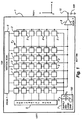
- FIG. 1 is a top view of an IC device 1 that includes a generally planar, multiple pixel, multiple row/column, array 3 having a relatively large number of solid state capacitive sensor cells, or nodes 2, that operate to provide a serial signal electrical output 10 that comprises a multiple pixel fingerprint pattern, or electrical signal picture of a fingerprint. As shown, FIG. 1 is taken in the X-Y plane.
- Array 3 contains the number N of horizontal or X-direction extending rows of individual nodes 2. Each row has the number M of individual nodes 2 therein. Array 3 thus contains the number M of vertically or Y-direction extending columns of individual nodes 2, and each column has the number N of individual nodes 2 therein.
- the numbers N and M are integers that may or may not be equal to each other.
- the number of individual picture elements, pixels, nodes, or cells 2 within array 3 is quite large for fingerprint pattern acquisition, and equals the product of MxN.
- An example is 512x512 pixels, nodes, or cells 2 within array 3, array 3 being of a physical size of about 20 mm to about 25 mm.
- FIG. 2 shows a fingertip 18 in physical contact with the upper and active surface 125 of array 3.
- each individual cell 2 that is within array 3 is addressable by virtue of each cell being physically located at a unique intersection of a row/column of array 3.
- the manner in which the individual cells 2 of array 3 are addressed and read out in order to digitize a fingerprint pattern are well known to those of skill in the art, and do not form a limitation on this invention.
- IC device 1 includes a horizontal scanning stage, or network 6, and a vertical scanning stage or network 5 for sequentially interrogating, or reading, one cell 2 at a time during fingerprint pattern acquisition according to a predetermined scanning pattern.
- stages 5 and 6 comprise shift registers, or decoders, that operate to interrogate the FIG. 2 outputs 17 of cells 2 in a time sequence.
- IC device 1 also includes a supply/logic stage or network 7 that operates to supply the IC device components, including all cells 2, with necessary operating voltages, and to control the sequence of steps that are necessary for operation of IC device 1.
- a DC voltage source 12 provides a DC reference voltage Vr that is referenced to ground potential at 100.
- a buffer 8 is connected to the outputs 17 of all cells 2. Output 10 of buffer 8 comprises the sequentially arranged output signal of IC device 1, the signal at output 10 being controlled by operation of scanning stages 5 and 6.
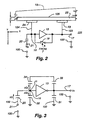
- FIG. 2 schematically shows the circuit of a single cell 2 of the array 3 of FIG. 1. All cells 2 are generally identical in construction and arrangement. Each cell 2 includes a low-power, signal inverting, node-amplifier 13 having an exemplary gain from about 3000 to about 4000.
- Terminal 21 comprises the input to the circuit of a cell 2, and terminal 21 and input capacitor 20 connect to input 16 of amplifier 13.
- Terminal 17 comprises the output of cell 2 and its amplifier 13.
- Each cell 2 also includes two X-Y planar armatures, or metal capacitor plates 23,24, that are of a generally equal X-Y area, and that are horizontally or X-direction spaced from each other within a common X-Y horizontal plane.
- a thin dielectric layer 25 covers capacitor plates 23,24, and the upper horizontal surface 125 of layer 25 provides an active array surface for physical contact by the skin surface 18 of a finger whose fingerprint is to be sensed, determined or acquired.
- Dielectric layer 25 may cover the entire face of the upper portion of IC device I that includes array 3 and its individual cells 2.
- a fingertip 18 In use for fingerprint pattern acquisition, a fingertip 18 is placed on the upper surface 125 of the dielectric layer 25 of array 3. Skin surface 18 thereby forms an armature, or electrode, that vertically overlies and faces the top, X-Y planar, surfaces of capacitor plates 23,24. Skin surface 18 operates to define with plates 23,24 a first capacitor 34, as shown in FIG. 3, and a second capacitor 33 as shown in FIG. 3. Series connected compound capacitors 33,34 are connected in negative feedback fashion from amplifier output 17 to amplifier input 16.
- Each FIG. 2 node-amplifier 13 also includes a normally-open start, reset, or control switch 19, preferably in the form of a MOS switch.
- Switch 19 selectively and momentarily operates to short amplifier input 16 to amplifier output 17.
- Switch 19 is controlled by a control signal "R" that is provided by the supply and logic unit 7 of FIG. 1.
- R control signal
- switches 19 of all array cells 2 are momentarily closed, and the voltage level at all cell inputs 21 is thus maintained at a constant magnitude. In this way, the input voltage of all cells 2 is brought to the same potential as the cell's output voltage.
- supply and logic unit 7 operates to open all reset switches 19, and to supply all cell inputs 21 with a step voltage that is equal in magnitude to reference voltage Vr.
- An electrical charge is now induced at each of the cell input capacitors 20, thus permitting the reading of the local and individual Z-direction cell distances "d" that exist between a cell's capacitor plates 23,24 and the overlying skin surface 18 of the cell.
- Scanning stages 5,6 of FIG. 1 now operate to sequentially enable the reading or interrogation of the many cells 2 within array 3.
- buffer 8 operates to sequentially provide an output 10 in the form of a sequence of gray levels of voltage that provide a three-dimensional readout, and display of the skin surface 18 of the finger that is currently resident on the top surface 125 of array 3.
- FIG. 3 is an equivalent circuit of the single cell circuit shown in FIG. 2.
- the input capacitance of amplifier 13 is shown at 30, the output capacitance of amplifier 13 is shown at 31, and the two above-mentioned series connected and skin-sensitive capacitors are shown at 33,34.
- the gain of each amplifier 16 can be increased in order to provide an output signal from the FIG. 1 array that comprises the corrected shape 170 shown in the various areas of FIGS. 5A-51.
- this increased gain feature is not required, since this corrected shape can also be calculated over the fingertip's complicated fingerprint pattern because the center of mass of the group of objects comprising the fingerprint is positioned in the center of the group of objects.
- the increased gain feature is desired it is implemented by a step change in the magnitude of the voltage Vr of FIG. 1.
- the output 17 of all cells 2, or node-amplifiers 13 is a picture-signal that appears as a bright blob 170 that is positioned on a dark background, as is shown in FIGS. 5A-51.
- the position of this blob 170 within the picture encodes the contact area/position of finger 18 with the top surface 125 of the capacitance touchpad.
- This blob output signal function 170 can also be achieved by a construction and arrangement that ensures that the resolution of the cell-array matrix is low.
- FIG. 4 is a flowchart that shows a fingerprint pattern acquisition process, whereby the arrangement of FIGS. 1-3 is used in a low-gain mode during an initial log-on by a computer user, which user thereafter uses the capacitance touchpad construction and arrangement of the present invention to generate a cursor/pointer screen direction/movement control signal, and/or a switch on/off the touchpad signal.
- the buffer output 10 from array 3 of FIG. 1 is connected to a processing unit 160.
- start switches 19 of all cells 2 are momentarily closed, thereafter reference step pulse voltage Vr is applied to all amplifier inputs 21, and thereafter all cell outputs 17 are presented to buffer output 10 in accordance with a sequence that is established by vertical and horizontal scan networks 5,6.
- Vr reference step pulse voltage
- all cell outputs 17 are presented to buffer output 10 in accordance with a sequence that is established by vertical and horizontal scan networks 5,6.
- the fingerprint pattern of fingertip 18 is presented as an input 10 to processing unit 160.
- Connection 10 between array 3 and processing unit 160 is shown to be bi-directional in order to signify the changing of array sensitivity when changing from fingerprint acquisition to touchpad operation.
- Reference memory 161 contains a number of previously-stored fingerprint patterns; for example, one fingerprint pattern for each authorized user.
- a similar computing unit compares input 10 to the patterns that are contained in memory 162, and when a pattern match is detected, the identity of the current touchpad/computer user is recorded in working memory 164.
- step 165 enables use of the touchpad of this invention as a joystick-type touchpad.
- this joystick-type use of the touchpad takes place in a high-gain mode of FIGS. 1 -3.
- the composite outputs 17 of all array cells 2 comprises an electronic picture-signal that appears as a bright blob that is positioned on a dark background.
- FIGS. 5A through 51 show such a picture-signal for various positions of a fingertip 18 on array surface 125.
- the position of bright blob 170 in each of these figures corresponds to the contact area, or position of fingertip 18 with the top surface 125 of the capacitance touchpad.
- the center of each blob 170 is shown at 470.
- a Z-direction depression of fingertip 18 when it is in any of the FIG. 5A-5I positions modifies or enlarges the mass of bright blob signal 170, so as to provide a switch-closed signal.
- the fingertip center 470 is located in a mid-position on array surface 125, and in this position, no cursor movement is produced.
- the relatively large mass, or size of blob 170 that is shown in FIG. 5A is indicative of a switch-closed condition that is produced by pressing fingertip 18 vertically down onto array surface 125.
- FIG. 6 represents the Y-direction pitching of fingertip 18 end to end on surface 125.
- a bright blob 170 is produced, as is shown in FIGS. 5B and 5C. That is, the pitching of fingertip 18 downward in FIG. 6 produces the condition shown in FIG. 58, and upward cursor movement occurs, as is represented by arrow 171.
- FIG. 6 pitching of fingertip 18 upward produces the condition of FIG. 5C
- downward cursor movement as represented by arrow 172 occurs.
- FIG. 7 represents the X-direction rolling of fingertip 18 side to side on surface 125.
- a blob 170 is produced, as is shown in FIGS. 5E and 5D. That is, the rolling of fingertip 18 to the left in FIG. 7 produces the condition shown in FIG. 5E, and leftward cursor movement occurs, as is represented by arrow 173. However, when the rolling of fingertip 18 to the right produces the condition of FIG. 5D, rightward cursor movement as represented by arrow 174 occurs.
- FIGS. 5F and 5G show how diagonal cursor movements 175 and 176 occur as a result of the combined pitch and roll of fingertip 18 in one diagonal direction on surface 125
- FIGS. 5H and 5I s show how diagonal cursor movements 177 and 178 occur as a result of the combined pitch and roll of fingertip 18 in an orthogonal diagonal direction on surface 125.
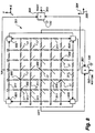
- FIG. 8 is a top view that is taken in the X-Y plane showing an embodiment of this invention having four corner-located current mirrors and adders, or current-buffers 601-604, wherein the amplifier output 17 of each of 25 node-cells 2 is connected to a different one of the 25 nodes 300 of a resistive network 301, each node 300 being established by the intersection of a cell-column C1-C5 with a cell-row R1-R5.
- Resistive network 301 comprises a pseudo-resistive network having four corner-located current mirrors and adders, or current buffers 601-604, that operates to detect the mass or area and the centroid 470 of the blob signals 170 that are shown in the various ones of figures 5.
- FIG. 9 shows one individual resistor-network node 300 connected to the output 17 of its corresponding individual FIG. 2 node-amplifier.
- FIG. 9 also shows four resistors 311 that connect this node 300 to its four adjacent nodes 300.
- node 300 of FIG. 9 is the node that is formed by the intersection of node-column C2 and node-row R2
- its amplifier output 17 is the output of the FIG. 2 amplifier that is associated with the FIG. 1 cell that is located at the intersection of cell-column 2 and cell-row 2.
- array 3 of FIGS. 1-3 is first used to acquire user-fingerprint-ID during log-on, as was described relative to FIG.4. Thereafter, output 17 of each of the 25 cell-amplifiers of FIG. 2 is connected to a corresponding one of the 25 resistor-nodes 300 shown in FIG. 8.
- electrical outputs 302 and 303 respectively, provide the X-direction component and the Y-direction component of an output signal that defines the user's desired cursor/pointer screen movement direction.
- signals 302,303 are used to control movement of a cursor/pointer across a TV or monitor screen, with this movement being continuous by virtue of a static/non-moving position of a fingertip 18 on the surface of the FIG. 8 touchpad.
- outputs 302,303 provide an analog value which is proportional to the zero and first moment of the 2D-pattern.
- output 302 is essentially of zero magnitude, whereas output 303 is of a given magnitude and a given polarity or signal sense. As a result, upward cursor movement 171 is produced. If it is now assumed that the fingertip position produces bright blob 170 of FIG. 5C, then output 302 remains essentially zero, whereas output 303 is now of a given magnitude, but of an opposite polarity or signal sense, and downward cursor movement 172 results. In a like manner, outputs 302,303 can be related to the cursor movements as explained relative to the remaining ones of figures 5.
- the user achieves a desired cursor/pointer movement by sidewise rolling movement of fingertip 18, represented by arrow 304, and/or by lengthwise end to end pitching of fingertip 18, represented by arrow 305.
- each individual cell output 17 of the array is serially scanned.
- the touchpad's individual cell outputs 17 are not scanned. Rather, each individual cell output 17 is connected to an individual node 300 of row/column resistive network 301.
- Array 301 generates a X-direction cursor/pointer movement command 302, that is a horizontal left/right screen movement command, as fingertip 18 is moved, or rolled, sideways on the upper horizontal surface of array 301, this movement being indicated by arrow 305.
- Array 301 generates a Y-direction cursor/pointer movement command 303 that is a vertical up/down screen movement command, as fingertip 18 is moved, or pitched, end to end on the horizontal upper surface of array 301, this movement being indicated by arrow 304.
- Array 301 also generates a switch output or Z-command output as long as fingertip 18 is pressed vertically down onto the general geometric center of the current position of fingertip 18 on the horizontal upper surface of array 301.
- one step in enabling touchpad operation may be to switch each FIG. 2 node-amplifier 13 from low gain to high gain by operation of a change in the magnitude of the voltage Vr of FIG. 1.
- the composite electrical outputs 17 of all node-amplifiers 13 can be described as an electronic array picture having a blob 170 that is located on a dark background wherein the central position 470 of this blob on the dark background corresponds to the area of contact of fingertip 18 with the top horizontal surface of array 301.
- the first-moment coordinates of the position of this blob 170, or brightness function within this electronic picture encodes the X and Y displacement or finger position on the array's top surface, while the zero-moment value of bright blob 170 encodes the finger's downward, or Z-direction pressure function.
- Networks 307 and 308 of FIG. 8 operate to determine the first-moment-coordinates and the zero-moment-value that are encoded within this electronic picture.
- the entire electronic image of the array that is all cell-amplifier output signals 17, is transferred into a computation system where the first-moment-coordinates and the zero-moment-value (also called “mass” and “centroid") are calculated using hardware or software.
- analog computation may be performed on the FIG. 8 analog values that are proportional to the zero and first moment of the 2-D pattern.
- the resistor-network embodiment of the invention utilizes the first above-mentioned technique by way of the following hardware.
- the two-dimensional (2D) electronic signal-picture, output, or pattern of array 3 which encodes the touching function of fingertip 18 on the array's upper surface, is injected into nodes 300 of the 2D resistive network 301 of FIG. 8.
- Networks 307,308,309 then function to detect the centroid and the mass of this array output signal.
- the functions centroid and mass are calculated simultaneously by the FIG. 8 arrangement.
- each node 300 is connected to its adjacent nodes 300 by way of a resistor 311. While the resistance values, or magnitudes of resistors 3 11 are not critical, all resistors 311 should be of generally the same resistance value or magnitude. In addition, and as stated above, as a feature of the invention, resistors 311 1 are implemented by way of MOS transistors.
Landscapes
- Engineering & Computer Science (AREA)
- Theoretical Computer Science (AREA)
- General Engineering & Computer Science (AREA)
- General Physics & Mathematics (AREA)
- Physics & Mathematics (AREA)
- Human Computer Interaction (AREA)
- Computer Hardware Design (AREA)
- Computer Security & Cryptography (AREA)
- Software Systems (AREA)
- Multimedia (AREA)
- Measurement Of Length, Angles, Or The Like Using Electric Or Magnetic Means (AREA)
- Image Input (AREA)
- Position Input By Displaying (AREA)
- Measurement Of The Respiration, Hearing Ability, Form, And Blood Characteristics Of Living Organisms (AREA)
Claims (11)
- Pavé tactile capacitif pour fournir un signal de sortie électrique pour commander sélectivement le déplacement d'un repère visuel de pointeur sur un écran d'affichage bidimensionnel comprenant :une pluralité N de cellules de détection capacitives individuelles (2) disposées en un premier réseau bidimensionnel de rangées/colonnes (3), le premier réseau (3) comprenant N intersections de rangées et de colonnes et le premier réseau (3) occupant une surface généralement plane qui est adaptée à coopérer avec une extrémité de doigt humain pour fournir un signal de sortie pour commander le déplacement du repère, chaque cellule de détection individuelle (2) ayant un signal de sortie spécifique qui varie en fonction de la relation de position avec une extrémité de doigt humain ;une pluralité N de noeuds résistifs (300) individuels disposés en un second réseau bidimensionnel de rangées et de colonnes (301), le second réseau ayant N intersections de rangées et de colonnes dans une configuration qui correspond aux N intersections de rangées et de colonnes du premier réseau ;un moyen de circuit reliant chaque signal de sortie spécifique des cellules de détection (2) à l'un correspondant des noeuds résistifs (300) du second réseau ;un premier moyen de calcul connecté au second réseau (301) pour calculer un signal de sortie central en fonction de la position de l'extrémité de doigt humain sur la surface plane du premier réseau (3) ; etun premier moyen de sortie connecté au premier moyen de calcul et fournissant un signal de commande de déplacement de repère en fonction du signal de sortie central.
- Pavé tactile capacitif selon la revendication 1, comprenant :un second moyen de calcul connecté au second réseau pour calculer un signal de sortie de masse en fonction de la surface occupée par l'extrémité de doigt humain sur la surface plane ; etun second moyen de sortie connecté au second moyen de calcul fournissant un signal de commutation en marche/arrêt en fonction du signal de sortie de masse.
- Pavé tactile capacitif selon la revendication 1, dans lequel le premier réseau (3) a une surface de détection (125) ; adapté à recevoir l'extrémité de doigt humain et à commander le déplacement d'un repère d'indicateur en fonction de la position de l'extrémité de doigt humain sur la surface de détection.
- Pavé tactile capacitif selon la revendication 3, dans lequel chacune des N cellules de détection comprend un amplificateur ayant une entrée (16) d'amplificateur (13) et une sortie (17) d'amplificateur, une première et une seconde plaque de condensateur physiquement espacées (23, 24) étant associées à la surface de détection (125).
- Pavé tactile capacitif selon la revendication 3, comprenant :un second moyen de calcul connecté au second réseau (301) pour calculer un signal de sortie de masse en fonction de la surface occupée par l'extrémité de doigt humain sur la surface de détection (125) ; etun second moyen de sortie connecté au second moyen de calcul et fournissant un signal de commutation en marche/arrêt en fonction du signal de sortie de masse.
- Pavé tactile capacitif selon la revendication 3, comprenant en outre un moyen d'autorisation d'utilisateur connecté au premier réseau et actionnable pour produire une empreinte digitale d'utilisateur pour comparaison avec des empreintes digitales d'utilisateurs autorisés, et pour permettre ainsi à l'actionnement du pavé tactile de commander le déplacement du curseur en fonction de la position de l'extrémité de doigt humain sur la surface de détection (125).
- Pavé tactile capacitif selon la revendication 1, dans lequel le premier réseau (3) comprend :une surface de détection (125) diélectrique généralement plane et ayant une pluralité de portions de surface ;la surface de détection (125) étant adaptée à être physiquement touchée par l'extrémité d'un doigt humain ;la pluralité N de cellules de détection étant associées aux portions de surface ;les cellules de détection (2) étant disposées en un réseau de cellules ayant R rangées et C colonnes, les rangées et colonnes formant RC intersections, une cellule de détection étant disposée au niveau de chaque intersection et au niveau d'une portion de surface correspondante ;chacune des cellules de détection (2) comprenant un amplificateur (13) ayant une entrée d'amplificateur (16) et une sortie d'amplificateur (17) ;chacune des cellules de détection (2) étant associée à une première (24) et une seconde (23) plaques de condensateur physiquement espacées mais isolées de la portion de surface correspondante ;chacune des cellules de détection (2) comprenant la première plaque de condensateur (24) connectée à l'entrée d'un amplificateur (16) et la seconde plaque de condensateur (23) connectée à la sortie (17) de l'amplificateur pour fournir ainsi une entrée négative au signal de réaction d'amplificateur de sortie en fonction du toucher par l'extrémité d'un doigt humain de la portion de surface correspondante.
- Pavé tactile capacitif selon la revendication 7, dans lequel la pluralité N de noeuds résistifs est agencée selon un réseau bidimensionnel (301) comprenant R rangées et C colonnes, les rangées et les colonnes formant RC intersections, un noeud résistif étant disposé à chaque intersection ;
chaque sortie d'amplificateur étant connecté à l'un correspondant des noeuds résistifs. - Pavé tactile capacitif selon la revendication 8, dans lequel R et C sont des entiers.
- Pavé tactile capacitif selon la revendication 4, comprenant en outre :un moyen d'autorisation d'utilisateur connecté au premier réseau, actionnable pour amener les amplificateurs (13) des cellules de détection à fonctionner dans un mode à faible gain, actionnable pour produire une empreinte digitale d'utilisateur pour comparaison avec des empreintes digitales mémorisées d'utilisateurs autorisés, et actionnable par suite d'une comparaison détectée pour amener des amplificateurs des cellules de détection à fonctionner dans un mode à fort gain et pour amener les amplificateurs de cellules de détection à permettre un fonctionnement du pavé tactile destiné à être utilisé pour commander le déplacement du curseur en fonction de la position d'une extrémité de doigt humain sur la surface de détection.
- Pavé tactile capacitif selon la revendication 10, dans lequel la pluralité N de cellules de détection de capacitives (2) et la pluralité N de noeuds résistifs (300) sont intégrés dans un ensemble monolithique.
Priority Applications (1)
| Application Number | Priority Date | Filing Date | Title |
|---|---|---|---|
| EP06075705A EP1669847A2 (fr) | 1998-01-22 | 1999-01-20 | Pavé tactile avec contrôle du mouvement du curseur/pointeur d'écran |
Applications Claiming Priority (2)
| Application Number | Priority Date | Filing Date | Title |
|---|---|---|---|
| US09/012,065 US6392636B1 (en) | 1998-01-22 | 1998-01-22 | Touchpad providing screen cursor/pointer movement control |
| US12065 | 1998-01-22 |
Related Child Applications (1)
| Application Number | Title | Priority Date | Filing Date |
|---|---|---|---|
| EP06075705A Division EP1669847A2 (fr) | 1998-01-22 | 1999-01-20 | Pavé tactile avec contrôle du mouvement du curseur/pointeur d'écran |
Publications (3)
| Publication Number | Publication Date |
|---|---|
| EP0932117A2 EP0932117A2 (fr) | 1999-07-28 |
| EP0932117A3 EP0932117A3 (fr) | 2000-07-26 |
| EP0932117B1 true EP0932117B1 (fr) | 2006-04-12 |
Family
ID=21753213
Family Applications (2)
| Application Number | Title | Priority Date | Filing Date |
|---|---|---|---|
| EP99300408A Expired - Lifetime EP0932117B1 (fr) | 1998-01-22 | 1999-01-20 | Tablette à touche pour commander le mouvement de curseur sur un écran |
| EP06075705A Withdrawn EP1669847A2 (fr) | 1998-01-22 | 1999-01-20 | Pavé tactile avec contrôle du mouvement du curseur/pointeur d'écran |
Family Applications After (1)
| Application Number | Title | Priority Date | Filing Date |
|---|---|---|---|
| EP06075705A Withdrawn EP1669847A2 (fr) | 1998-01-22 | 1999-01-20 | Pavé tactile avec contrôle du mouvement du curseur/pointeur d'écran |
Country Status (4)
| Country | Link |
|---|---|
| US (1) | US6392636B1 (fr) |
| EP (2) | EP0932117B1 (fr) |
| JP (1) | JP4209984B2 (fr) |
| DE (1) | DE69930774T2 (fr) |
Cited By (7)
| Publication number | Priority date | Publication date | Assignee | Title |
|---|---|---|---|---|
| US8416209B2 (en) | 2004-05-06 | 2013-04-09 | Apple Inc. | Multipoint touchscreen |
| US8451244B2 (en) | 2006-06-09 | 2013-05-28 | Apple Inc. | Segmented Vcom |
| US8493330B2 (en) | 2007-01-03 | 2013-07-23 | Apple Inc. | Individual channel phase delay scheme |
| US8552989B2 (en) | 2006-06-09 | 2013-10-08 | Apple Inc. | Integrated display and touch screen |
| US8743300B2 (en) | 2010-12-22 | 2014-06-03 | Apple Inc. | Integrated touch screens |
| US9244561B2 (en) | 2006-06-09 | 2016-01-26 | Apple Inc. | Touch screen liquid crystal display |
| US9710095B2 (en) | 2007-01-05 | 2017-07-18 | Apple Inc. | Touch screen stack-ups |
Families Citing this family (190)
| Publication number | Priority date | Publication date | Assignee | Title |
|---|---|---|---|---|
| JP4175662B2 (ja) | 1996-01-08 | 2008-11-05 | インパルス ダイナミクス エヌ.ヴイ. | 電気的筋肉制御装置 |
| US8321013B2 (en) * | 1996-01-08 | 2012-11-27 | Impulse Dynamics, N.V. | Electrical muscle controller and pacing with hemodynamic enhancement |
| US9289618B1 (en) | 1996-01-08 | 2016-03-22 | Impulse Dynamics Nv | Electrical muscle controller |
| US7167748B2 (en) | 1996-01-08 | 2007-01-23 | Impulse Dynamics Nv | Electrical muscle controller |
| US8825152B2 (en) | 1996-01-08 | 2014-09-02 | Impulse Dynamics, N.V. | Modulation of intracellular calcium concentration using non-excitatory electrical signals applied to the tissue |
| US9713723B2 (en) | 1996-01-11 | 2017-07-25 | Impulse Dynamics Nv | Signal delivery through the right ventricular septum |
| KR100595926B1 (ko) | 1998-01-26 | 2006-07-05 | 웨인 웨스터만 | 수동 입력 통합 방법 및 장치 |
| US7808479B1 (en) * | 2003-09-02 | 2010-10-05 | Apple Inc. | Ambidextrous mouse |
| US6610917B2 (en) | 1998-05-15 | 2003-08-26 | Lester F. Ludwig | Activity indication, external source, and processing loop provisions for driven vibrating-element environments |
| US6950539B2 (en) * | 1998-09-16 | 2005-09-27 | Digital Persona | Configurable multi-function touchpad device |
| US6671392B1 (en) * | 1998-12-25 | 2003-12-30 | Nippon Telegraph And Telephone Corporation | Fingerprint recognition apparatus and data processing method |
| BR0009403A (pt) * | 1999-02-04 | 2001-11-27 | Technion Res & Dev Foundation | Método de expansão/conservação das células detronco hemopoiéticas indiferenciadas ou dascélulas progenitoras, método de preparação deum meio condicionado de célula estomacal útil naexpansão/conservação das células de troncohemopoiéticas indiferenciadas ou das célulasprogenitoras, método de transplante de célulasde tronco hemopoiéticas indiferenciadas ou decélulas progenitoras em um recipiente, tampão debiorreator e biorreator |
| US8346363B2 (en) | 1999-03-05 | 2013-01-01 | Metacure Limited | Blood glucose level control |
| US8700161B2 (en) | 1999-03-05 | 2014-04-15 | Metacure Limited | Blood glucose level control |
| US9101765B2 (en) * | 1999-03-05 | 2015-08-11 | Metacure Limited | Non-immediate effects of therapy |
| US8019421B2 (en) | 1999-03-05 | 2011-09-13 | Metacure Limited | Blood glucose level control |
| US8666495B2 (en) | 1999-03-05 | 2014-03-04 | Metacure Limited | Gastrointestinal methods and apparatus for use in treating disorders and controlling blood sugar |
| EP1079325B1 (fr) * | 1999-08-25 | 2006-04-05 | Swatch Ag | Montre comprenant un dispositif de commande sans contact d'un curseur d'ordinateur |
| LU90437B1 (de) * | 1999-09-08 | 2001-03-09 | Iee Sarl | Sensoreinrichtung und Verfahren zur Abfrage einer Sensoreinrichtung |
| GB2357335B (en) * | 1999-12-17 | 2004-04-07 | Nokia Mobile Phones Ltd | Fingerprint recognition and pointing device |
| US7239227B1 (en) * | 1999-12-30 | 2007-07-03 | Upek, Inc. | Command interface using fingerprint sensor input system |
| NO316482B1 (no) * | 2000-06-09 | 2004-01-26 | Idex Asa | Navigasjonsverktöy for kobling til en skjerminnretning |
| WO2002019084A1 (fr) * | 2000-08-01 | 2002-03-07 | Yongsun Kim | Systeme de bloc a effleurement |
| KR100698898B1 (ko) * | 2000-08-03 | 2007-03-22 | 한국터치스크린(주) | 터치판넬 |
| US7184026B2 (en) * | 2001-03-19 | 2007-02-27 | Avago Technologies Ecbu Ip (Singapore) Pte. Ltd. | Impedance sensing screen pointing device |
| DE10120067C1 (de) | 2001-04-24 | 2002-06-13 | Siemens Ag | Mobiles Kommunikationsendgerät |
| US20020176611A1 (en) * | 2001-05-23 | 2002-11-28 | Dong Mimi C. | Fingerprint addressing system and method |
| FR2832240A1 (fr) * | 2001-11-13 | 2003-05-16 | St Microelectronics Sa | Element de detection tactile, procede mettant en oeuvre un tel element de detection tactile, et appareil incorporant cet element |
| US6927581B2 (en) * | 2001-11-27 | 2005-08-09 | Upek, Inc. | Sensing element arrangement for a fingerprint sensor |
| US6762752B2 (en) * | 2001-11-29 | 2004-07-13 | N-Trig Ltd. | Dual function input device and method |
| KR20030079212A (ko) * | 2002-04-02 | 2003-10-10 | 김원찬 | 인체접촉 감지장치 |
| US7184009B2 (en) * | 2002-06-21 | 2007-02-27 | Nokia Corporation | Display circuit with optical sensor |
| US11275405B2 (en) | 2005-03-04 | 2022-03-15 | Apple Inc. | Multi-functional hand-held device |
| US7656393B2 (en) | 2005-03-04 | 2010-02-02 | Apple Inc. | Electronic device having display and surrounding touch sensitive bezel for user interface and control |
| AU2003250490A1 (en) * | 2002-08-23 | 2004-03-11 | Pfizer Products Inc. | Apparatus for dispensing articles |
| US7358963B2 (en) * | 2002-09-09 | 2008-04-15 | Apple Inc. | Mouse having an optically-based scrolling feature |
| FR2850478B1 (fr) * | 2003-01-29 | 2005-04-08 | Sagem | Dispositif de controle d'acces a fonction de capteur d'empreintes digitales |
| DE602004027705D1 (de) | 2003-02-10 | 2010-07-29 | N trig ltd | Berührungsdetektion für einen digitalisierer |
| US11439815B2 (en) | 2003-03-10 | 2022-09-13 | Impulse Dynamics Nv | Protein activity modification |
| WO2004080533A1 (fr) | 2003-03-10 | 2004-09-23 | Impulse Dynamics Nv | Appareil et procede d'application de signaux electriques pour modifier l'expression genique dans le tissu cardiaque |
| KR100964559B1 (ko) * | 2003-04-25 | 2010-06-21 | 삼성전자주식회사 | 지문 인식장치 |
| GB2401979B (en) * | 2003-05-21 | 2007-03-21 | Research In Motion Ltd | Apparatus and method of input and finger print recognition on a handheld electronic device |
| EP1487114B1 (fr) * | 2003-05-28 | 2006-09-20 | Freescale Semiconductor, Inc. | Le clavier |
| WO2004112448A2 (fr) * | 2003-06-13 | 2004-12-23 | Semtech Corporation | Capteur pour dispositif de pointage de pave tactile capacitif |
| NZ560223A (en) * | 2003-06-23 | 2008-12-24 | Sony Pictures Entertainment | Fingerprinting of data |
| CN1856338B (zh) | 2003-07-21 | 2012-11-14 | 超治疗有限公司 | 用于治疗疾病和控制血糖的胃肠方法和装置 |
| CN100520687C (zh) * | 2003-07-21 | 2009-07-29 | 皇家飞利浦电子股份有限公司 | 便携式设备和用于便携式设备的触敏显示器 |
| US6939736B2 (en) * | 2003-07-31 | 2005-09-06 | Texas Instruments Incorporated | Ideal operational amplifier layout techniques for reducing package stress and configurations therefor |
| FR2859525B1 (fr) * | 2003-09-09 | 2006-06-02 | Delphi Tech Inc | Commutateur capacitif glissant |
| US7109977B2 (en) * | 2003-10-05 | 2006-09-19 | T2D, Inc. | Slipcover touch input apparatus for displays of computing devices |
| US8352031B2 (en) | 2004-03-10 | 2013-01-08 | Impulse Dynamics Nv | Protein activity modification |
| US11779768B2 (en) | 2004-03-10 | 2023-10-10 | Impulse Dynamics Nv | Protein activity modification |
| US8131026B2 (en) | 2004-04-16 | 2012-03-06 | Validity Sensors, Inc. | Method and apparatus for fingerprint image reconstruction |
| US8358815B2 (en) | 2004-04-16 | 2013-01-22 | Validity Sensors, Inc. | Method and apparatus for two-dimensional finger motion tracking and control |
| US8229184B2 (en) | 2004-04-16 | 2012-07-24 | Validity Sensors, Inc. | Method and algorithm for accurate finger motion tracking |
| US8165355B2 (en) * | 2006-09-11 | 2012-04-24 | Validity Sensors, Inc. | Method and apparatus for fingerprint motion tracking using an in-line array for use in navigation applications |
| US8447077B2 (en) | 2006-09-11 | 2013-05-21 | Validity Sensors, Inc. | Method and apparatus for fingerprint motion tracking using an in-line array |
| US8077935B2 (en) | 2004-04-23 | 2011-12-13 | Validity Sensors, Inc. | Methods and apparatus for acquiring a swiped fingerprint image |
| US8175345B2 (en) | 2004-04-16 | 2012-05-08 | Validity Sensors, Inc. | Unitized ergonomic two-dimensional fingerprint motion tracking device and method |
| TWI267789B (en) * | 2004-06-30 | 2006-12-01 | Au Optronics Corp | Transparent touch panel for recognizing fingerprint |
| WO2006002661A1 (fr) * | 2004-06-30 | 2006-01-12 | Freescale Semiconductor, Inc. | Appareil a clavier pour saisie de signal |
| US20060007174A1 (en) * | 2004-07-06 | 2006-01-12 | Chung-Yi Shen | Touch control method for a drag gesture and control module thereof |
| WO2006006174A2 (fr) * | 2004-07-15 | 2006-01-19 | N-Trig Ltd. | Fenetre de poursuite pour systeme de numerisation |
| EP1787281A2 (fr) * | 2004-07-15 | 2007-05-23 | N-Trig Ltd. | Commutation automatique pour convertisseur analogique numerique a mode dual |
| JP4529012B2 (ja) * | 2004-07-16 | 2010-08-25 | アオイ電子株式会社 | ナノグリッパ装置 |
| US20060044280A1 (en) * | 2004-08-31 | 2006-03-02 | Huddleston Wyatt A | Interface |
| JP3931898B2 (ja) * | 2004-09-30 | 2007-06-20 | セイコーエプソン株式会社 | 個人認証装置 |
| WO2006041780A1 (fr) | 2004-10-04 | 2006-04-20 | Validity Sensors, Inc. | Groupes de detection d'empreintes digitales comprenant un substrat |
| EP1827571B1 (fr) | 2004-12-09 | 2016-09-07 | Impulse Dynamics NV | Modification de l'activite proteique |
| CN100368975C (zh) * | 2004-12-31 | 2008-02-13 | 义隆电子股份有限公司 | 电容式触控板及其检测方法 |
| GB2423808B (en) * | 2005-03-04 | 2010-02-17 | Ford Global Tech Llc | Motor vehicle control system for controlling one or more vehicle devices |
| US8244371B2 (en) | 2005-03-18 | 2012-08-14 | Metacure Limited | Pancreas lead |
| EP1898991B1 (fr) | 2005-05-04 | 2016-06-29 | Impulse Dynamics NV | Modification d'activite de proteine |
| US7710397B2 (en) * | 2005-06-03 | 2010-05-04 | Apple Inc. | Mouse with improved input mechanisms using touch sensors |
| US7244985B2 (en) * | 2005-09-06 | 2007-07-17 | Ememory Technology Inc. | Non-volatile memory array |
| CN100454224C (zh) * | 2005-12-28 | 2009-01-21 | 中兴通讯股份有限公司 | 一种具有虚拟键盘和手写协同输入功能的移动终端 |
| US8077147B2 (en) | 2005-12-30 | 2011-12-13 | Apple Inc. | Mouse with optical sensing surface |
| JP4669423B2 (ja) * | 2006-03-20 | 2011-04-13 | 富士通株式会社 | 電子機器、スクロール制御装置、およびプログラム |
| US7656392B2 (en) * | 2006-03-24 | 2010-02-02 | Synaptics Incorporated | Touch sensor effective area enhancement |
| KR101128803B1 (ko) * | 2006-05-03 | 2012-03-23 | 엘지전자 주식회사 | 이동 단말기, 및 터치 패널을 구비한 이동 단말기에서의입력신호 처리방법 |
| US20070273658A1 (en) * | 2006-05-26 | 2007-11-29 | Nokia Corporation | Cursor actuation with fingerprint recognition |
| JP4764281B2 (ja) * | 2006-08-07 | 2011-08-31 | 日本システム開発株式会社 | 位置測定センサ及び位置測定方法 |
| WO2008079596A1 (fr) * | 2006-12-19 | 2008-07-03 | 3M Innovative Properties Company | Capteur tactile comportant un réseau d'électrodes |
| US7973771B2 (en) * | 2007-04-12 | 2011-07-05 | 3M Innovative Properties Company | Touch sensor with electrode array |
| US8130203B2 (en) | 2007-01-03 | 2012-03-06 | Apple Inc. | Multi-touch input discrimination |
| US8542211B2 (en) * | 2007-01-03 | 2013-09-24 | Apple Inc. | Projection scan multi-touch sensor array |
| US8269727B2 (en) | 2007-01-03 | 2012-09-18 | Apple Inc. | Irregular input identification |
| US7855718B2 (en) | 2007-01-03 | 2010-12-21 | Apple Inc. | Multi-touch input discrimination |
| US8144129B2 (en) * | 2007-01-05 | 2012-03-27 | Apple Inc. | Flexible touch sensing circuits |
| US8970503B2 (en) * | 2007-01-05 | 2015-03-03 | Apple Inc. | Gestures for devices having one or more touch sensitive surfaces |
| TW200842681A (en) | 2007-04-27 | 2008-11-01 | Tpk Touch Solutions Inc | Touch pattern structure of a capacitive touch panel |
| US8107212B2 (en) * | 2007-04-30 | 2012-01-31 | Validity Sensors, Inc. | Apparatus and method for protecting fingerprint sensing circuitry from electrostatic discharge |
| US8290150B2 (en) * | 2007-05-11 | 2012-10-16 | Validity Sensors, Inc. | Method and system for electronically securing an electronic device using physically unclonable functions |
| US20080297174A1 (en) * | 2007-05-31 | 2008-12-04 | Sarangan Narasimhan | Capacitive sensing devices |
| JP5060845B2 (ja) * | 2007-06-27 | 2012-10-31 | 株式会社ジャパンディスプレイイースト | 画面入力型画像表示装置 |
| US8605050B2 (en) | 2007-08-21 | 2013-12-10 | Tpk Touch Solutions (Xiamen) Inc. | Conductor pattern structure of capacitive touch panel |
| DE102007052008A1 (de) | 2007-10-26 | 2009-04-30 | Andreas Steinhauser | Single- oder multitouchfähiger Touchscreen oder Touchpad bestehend aus einem Array von Drucksensoren sowie Herstellung solcher Sensoren |
| US8204281B2 (en) * | 2007-12-14 | 2012-06-19 | Validity Sensors, Inc. | System and method to remove artifacts from fingerprint sensor scans |
| US8276816B2 (en) | 2007-12-14 | 2012-10-02 | Validity Sensors, Inc. | Smart card system with ergonomic fingerprint sensor and method of using |
| TWI374379B (en) | 2007-12-24 | 2012-10-11 | Wintek Corp | Transparent capacitive touch panel and manufacturing method thereof |
| US8005276B2 (en) * | 2008-04-04 | 2011-08-23 | Validity Sensors, Inc. | Apparatus and method for reducing parasitic capacitive coupling and noise in fingerprint sensing circuits |
| US8116540B2 (en) | 2008-04-04 | 2012-02-14 | Validity Sensors, Inc. | Apparatus and method for reducing noise in fingerprint sensing circuits |
| US9019237B2 (en) * | 2008-04-06 | 2015-04-28 | Lester F. Ludwig | Multitouch parameter and gesture user interface employing an LED-array tactile sensor that can also operate as a display |
| CN101672660B (zh) * | 2008-04-10 | 2013-01-02 | 爱特梅尔公司 | 电容性位置传感器 |
| US8345014B2 (en) | 2008-07-12 | 2013-01-01 | Lester F. Ludwig | Control of the operating system on a computing device via finger angle using a high dimensional touchpad (HDTP) touch user interface |
| US8169414B2 (en) | 2008-07-12 | 2012-05-01 | Lim Seung E | Control of electronic games via finger angle using a high dimensional touchpad (HDTP) touch user interface |
| GB2474999B (en) | 2008-07-22 | 2013-02-20 | Validity Sensors Inc | System and method for securing a device component |
| US8604364B2 (en) * | 2008-08-15 | 2013-12-10 | Lester F. Ludwig | Sensors, algorithms and applications for a high dimensional touchpad |
| TWI378376B (en) * | 2008-09-23 | 2012-12-01 | Au Optronics Corp | Multi-touch positioning method for capacitive touch panel |
| TWI390452B (zh) | 2008-10-17 | 2013-03-21 | Acer Inc | 指紋感測裝置與方法以及具指紋感測之觸控裝置 |
| CN101727571B (zh) * | 2008-10-24 | 2012-09-19 | 宏碁股份有限公司 | 指纹感测装置以及具指纹感测的触控装置 |
| US8391568B2 (en) | 2008-11-10 | 2013-03-05 | Validity Sensors, Inc. | System and method for improved scanning of fingerprint edges |
| US9552154B2 (en) | 2008-11-25 | 2017-01-24 | Samsung Electronics Co., Ltd. | Device and method for providing a user interface |
| US9477396B2 (en) | 2008-11-25 | 2016-10-25 | Samsung Electronics Co., Ltd. | Device and method for providing a user interface |
| US8278946B2 (en) * | 2009-01-15 | 2012-10-02 | Validity Sensors, Inc. | Apparatus and method for detecting finger activity on a fingerprint sensor |
| US8600122B2 (en) | 2009-01-15 | 2013-12-03 | Validity Sensors, Inc. | Apparatus and method for culling substantially redundant data in fingerprint sensing circuits |
| US8374407B2 (en) | 2009-01-28 | 2013-02-12 | Validity Sensors, Inc. | Live finger detection |
| US10180746B1 (en) | 2009-02-26 | 2019-01-15 | Amazon Technologies, Inc. | Hardware enabled interpolating sensor and display |
| US9740341B1 (en) * | 2009-02-26 | 2017-08-22 | Amazon Technologies, Inc. | Capacitive sensing with interpolating force-sensitive resistor array |
| US8170346B2 (en) | 2009-03-14 | 2012-05-01 | Ludwig Lester F | High-performance closed-form single-scan calculation of oblong-shape rotation angles from binary images of arbitrary size using running sums |
| WO2010105507A1 (fr) | 2009-03-20 | 2010-09-23 | 宸鸿科技(厦门)有限公司 | Motif de circuit tactile capacitif et son procédé de fabrication |
| KR101666490B1 (ko) * | 2009-03-29 | 2016-10-14 | (주) 엔피홀딩스 | 격자형 전도성 감지부를 구비한 터치스크린 장치 |
| JP5288479B2 (ja) * | 2009-04-27 | 2013-09-11 | ルネサスエレクトロニクス株式会社 | 表示パネルドライバ |
| US8212159B2 (en) * | 2009-05-11 | 2012-07-03 | Freescale Semiconductor, Inc. | Capacitive touchpad method using MCU GPIO and signal processing |
| US8587531B2 (en) | 2009-06-10 | 2013-11-19 | Chunghwa Picture Tubes, Ltd. | Touch input device |
| US9785272B1 (en) | 2009-07-31 | 2017-10-10 | Amazon Technologies, Inc. | Touch distinction |
| US9244562B1 (en) | 2009-07-31 | 2016-01-26 | Amazon Technologies, Inc. | Gestures and touches on force-sensitive input devices |
| US20110055722A1 (en) * | 2009-09-02 | 2011-03-03 | Ludwig Lester F | Data Visualization Environment with DataFlow Processing, Web, Collaboration, Advanced User Interfaces, and Spreadsheet Visualization |
| US20110066933A1 (en) | 2009-09-02 | 2011-03-17 | Ludwig Lester F | Value-driven visualization primitives for spreadsheets, tabular data, and advanced spreadsheet visualization |
| CN102043498B (zh) * | 2009-10-15 | 2013-08-14 | 瑞鼎科技股份有限公司 | 触控装置 |
| US9274553B2 (en) | 2009-10-30 | 2016-03-01 | Synaptics Incorporated | Fingerprint sensor and integratable electronic display |
| US9336428B2 (en) | 2009-10-30 | 2016-05-10 | Synaptics Incorporated | Integrated fingerprint sensor and display |
| US9400911B2 (en) | 2009-10-30 | 2016-07-26 | Synaptics Incorporated | Fingerprint sensor and integratable electronic display |
| US8810524B1 (en) | 2009-11-20 | 2014-08-19 | Amazon Technologies, Inc. | Two-sided touch sensor |
| US8421890B2 (en) | 2010-01-15 | 2013-04-16 | Picofield Technologies, Inc. | Electronic imager using an impedance sensor grid array and method of making |
| US8866347B2 (en) | 2010-01-15 | 2014-10-21 | Idex Asa | Biometric image sensing |
| US8791792B2 (en) | 2010-01-15 | 2014-07-29 | Idex Asa | Electronic imager using an impedance sensor grid array mounted on or about a switch and method of making |
| US8934975B2 (en) | 2010-02-01 | 2015-01-13 | Metacure Limited | Gastrointestinal electrical therapy |
| US20110202934A1 (en) * | 2010-02-12 | 2011-08-18 | Ludwig Lester F | Window manger input focus control for high dimensional touchpad (htpd), advanced mice, and other multidimensional user interfaces |
| US9666635B2 (en) | 2010-02-19 | 2017-05-30 | Synaptics Incorporated | Fingerprint sensing circuit |
| US10146427B2 (en) | 2010-03-01 | 2018-12-04 | Nri R&D Patent Licensing, Llc | Curve-fitting approach to high definition touch pad (HDTP) parameter extraction |
| US8716613B2 (en) | 2010-03-02 | 2014-05-06 | Synaptics Incoporated | Apparatus and method for electrostatic discharge protection |
| US20110221684A1 (en) * | 2010-03-11 | 2011-09-15 | Sony Ericsson Mobile Communications Ab | Touch-sensitive input device, mobile device and method for operating a touch-sensitive input device |
| US9001040B2 (en) | 2010-06-02 | 2015-04-07 | Synaptics Incorporated | Integrated fingerprint sensor and navigation device |
| US9632344B2 (en) | 2010-07-09 | 2017-04-25 | Lester F. Ludwig | Use of LED or OLED array to implement integrated combinations of touch screen tactile, touch gesture sensor, color image display, hand-image gesture sensor, document scanner, secure optical data exchange, and fingerprint processing capabilities |
| US9626023B2 (en) | 2010-07-09 | 2017-04-18 | Lester F. Ludwig | LED/OLED array approach to integrated display, lensless-camera, and touch-screen user interface devices and associated processors |
| US8754862B2 (en) | 2010-07-11 | 2014-06-17 | Lester F. Ludwig | Sequential classification recognition of gesture primitives and window-based parameter smoothing for high dimensional touchpad (HDTP) user interfaces |
| US9950256B2 (en) | 2010-08-05 | 2018-04-24 | Nri R&D Patent Licensing, Llc | High-dimensional touchpad game controller with multiple usage and networking modalities |
| US8331096B2 (en) | 2010-08-20 | 2012-12-11 | Validity Sensors, Inc. | Fingerprint acquisition expansion card apparatus |
| US8538097B2 (en) | 2011-01-26 | 2013-09-17 | Validity Sensors, Inc. | User input utilizing dual line scanner apparatus and method |
| US8594393B2 (en) | 2011-01-26 | 2013-11-26 | Validity Sensors | System for and method of image reconstruction with dual line scanner using line counts |
| US20120204577A1 (en) | 2011-02-16 | 2012-08-16 | Ludwig Lester F | Flexible modular hierarchical adaptively controlled electronic-system cooling and energy harvesting for IC chip packaging, printed circuit boards, subsystems, cages, racks, IT rooms, and data centers using quantum and classical thermoelectric materials |
| US8797288B2 (en) | 2011-03-07 | 2014-08-05 | Lester F. Ludwig | Human user interfaces utilizing interruption of the execution of a first recognized gesture with the execution of a recognized second gesture |
| US9406580B2 (en) | 2011-03-16 | 2016-08-02 | Synaptics Incorporated | Packaging for fingerprint sensors and methods of manufacture |
| CN102866794A (zh) | 2011-06-15 | 2013-01-09 | 宸鸿光电科技股份有限公司 | 触控感测层及其制造方法 |
| CN102902394A (zh) * | 2011-07-28 | 2013-01-30 | 宸鸿科技(厦门)有限公司 | 触控面板以及其侦测方法 |
| US9052772B2 (en) | 2011-08-10 | 2015-06-09 | Lester F. Ludwig | Heuristics for 3D and 6D touch gesture touch parameter calculations for high-dimensional touch parameter (HDTP) user interfaces |
| US8810367B2 (en) * | 2011-09-22 | 2014-08-19 | Apple Inc. | Electronic device with multimode fingerprint reader |
| US10043052B2 (en) | 2011-10-27 | 2018-08-07 | Synaptics Incorporated | Electronic device packages and methods |
| US9823781B2 (en) | 2011-12-06 | 2017-11-21 | Nri R&D Patent Licensing, Llc | Heterogeneous tactile sensing via multiple sensor types |
| US10430066B2 (en) | 2011-12-06 | 2019-10-01 | Nri R&D Patent Licensing, Llc | Gesteme (gesture primitive) recognition for advanced touch user interfaces |
| US9195877B2 (en) | 2011-12-23 | 2015-11-24 | Synaptics Incorporated | Methods and devices for capacitive image sensing |
| US9785299B2 (en) | 2012-01-03 | 2017-10-10 | Synaptics Incorporated | Structures and manufacturing methods for glass covered electronic devices |
| TW201335821A (zh) * | 2012-02-20 | 2013-09-01 | Inv Element Inc | 內嵌式觸控電路裝置 |
| US9137438B2 (en) | 2012-03-27 | 2015-09-15 | Synaptics Incorporated | Biometric object sensor and method |
| US9268991B2 (en) | 2012-03-27 | 2016-02-23 | Synaptics Incorporated | Method of and system for enrolling and matching biometric data |
| US9251329B2 (en) | 2012-03-27 | 2016-02-02 | Synaptics Incorporated | Button depress wakeup and wakeup strategy |
| US9600709B2 (en) | 2012-03-28 | 2017-03-21 | Synaptics Incorporated | Methods and systems for enrolling biometric data |
| US9152838B2 (en) | 2012-03-29 | 2015-10-06 | Synaptics Incorporated | Fingerprint sensor packagings and methods |
| EP2836960B1 (fr) | 2012-04-10 | 2018-09-26 | Idex Asa | Détection biométrique |
| US9665762B2 (en) | 2013-01-11 | 2017-05-30 | Synaptics Incorporated | Tiered wakeup strategy |
| US8874396B1 (en) * | 2013-06-28 | 2014-10-28 | Cypress Semiconductor Corporation | Injected touch noise analysis |
| US9819344B2 (en) | 2013-08-30 | 2017-11-14 | Stmicroelectronics International N.V. | Dynamic element matching of resistors in a sensor |
| USD727194S1 (en) | 2014-01-21 | 2015-04-21 | Wimo Labs LLC | Bracelet |
| US9785279B2 (en) | 2014-01-31 | 2017-10-10 | Hewlett-Packard Development Company, L.P. | Touch distance based on a column weighted sensor value |
| CN204009771U (zh) * | 2014-08-06 | 2014-12-10 | 胡竞韬 | 一种触感型控制器 |
| CN104252277A (zh) * | 2014-09-18 | 2014-12-31 | 叶志 | 一种触摸面板阵列以及用于触摸面板阵列的扫描方法 |
| TWI575461B (zh) * | 2015-02-13 | 2017-03-21 | 比亞迪股份有限公司 | 指紋檢測電路及指紋檢測方法及電子裝置 |
| KR102093196B1 (ko) * | 2015-04-16 | 2020-04-14 | 삼성전자주식회사 | 지문 인식 기반 조작 방법 및 장치 |
| TWM520166U (zh) * | 2015-04-27 | 2016-04-11 | 瑞鼎科技股份有限公司 | 電容式指紋感測裝置 |
| TWI575464B (zh) * | 2015-06-04 | 2017-03-21 | 指紋卡公司 | 用於基於指紋的導移的方法及系統 |
| TWI619044B (zh) * | 2015-07-23 | 2018-03-21 | 瑞鼎科技股份有限公司 | 電容式指紋感測裝置及電容式指紋感測方法 |
| TWI591509B (zh) * | 2015-08-27 | 2017-07-11 | 瑞鼎科技股份有限公司 | 電容式指紋感測裝置及電容式指紋感測方法 |
| US11250307B2 (en) | 2017-03-23 | 2022-02-15 | Idex Biometrics Asa | Secure, remote biometric enrollment |
| US10282651B2 (en) | 2017-03-23 | 2019-05-07 | Idex Asa | Sensor array system selectively configurable as a fingerprint sensor or data entry device |
| WO2019116233A1 (fr) | 2017-12-12 | 2019-06-20 | Idex Asa | Source d'alimentation pour enregistrement biométrique avec indicateurs d'état |
| CN111954488B (zh) * | 2018-03-08 | 2024-08-06 | 生物隐形有限公司 | 心血管健康监测装置 |
| CN110828379A (zh) * | 2019-10-15 | 2020-02-21 | 深圳大学 | 一种薄膜晶体管的制造方法、薄膜晶体管及显示面板 |
| DE102020003923B3 (de) | 2020-06-30 | 2021-11-04 | Daimler Ag | Bedieneinheit mit einer berührungssensitiven Bedienfläche |
| CN119473054B (zh) * | 2025-01-11 | 2025-04-18 | 深圳市深普科技开发有限公司 | 触控板压力测量及触控振动系统及电子设备 |
Family Cites Families (18)
| Publication number | Priority date | Publication date | Assignee | Title |
|---|---|---|---|---|
| US3641431A (en) | 1968-10-01 | 1972-02-08 | Gleason Works | Method for inspecting and adjusting cutter blades |
| US4353056A (en) | 1980-06-05 | 1982-10-05 | Siemens Corporation | Capacitive fingerprint sensor |
| US4641350A (en) | 1984-05-17 | 1987-02-03 | Bunn Robert F | Fingerprint identification system |
| DE3544187A1 (de) | 1985-12-13 | 1987-06-19 | Flowtec Ag | Kapazitaetsmessschaltung |
| EP0343580B1 (fr) | 1988-05-24 | 1993-03-10 | Nec Corporation | Procédé et dispositif pour comparer les empreintes digitales |
| US4958129A (en) | 1989-03-07 | 1990-09-18 | Ade Corporation | Prealigner probe |
| GB2244164A (en) | 1990-05-18 | 1991-11-20 | Philips Electronic Associated | Fingerprint sensing |
| US5369228A (en) * | 1991-11-30 | 1994-11-29 | Signagraphics Corporation | Data input device with a pressure-sensitive input surface |
| US5543591A (en) | 1992-06-08 | 1996-08-06 | Synaptics, Incorporated | Object position detector with edge motion feature and gesture recognition |
| US5861583A (en) * | 1992-06-08 | 1999-01-19 | Synaptics, Incorporated | Object position detector |
| DE69324067T2 (de) | 1992-06-08 | 1999-07-15 | Synaptics Inc | Objekt-Positionsdetektor |
| US5543588A (en) | 1992-06-08 | 1996-08-06 | Synaptics, Incorporated | Touch pad driven handheld computing device |
| US5543590A (en) | 1992-06-08 | 1996-08-06 | Synaptics, Incorporated | Object position detector with edge motion feature |
| US5828773A (en) * | 1996-01-26 | 1998-10-27 | Harris Corporation | Fingerprint sensing method with finger position indication |
| US5859420A (en) * | 1996-02-12 | 1999-01-12 | Dew Engineering And Development Limited | Optical imaging device |
| DE69618559T2 (de) | 1996-02-14 | 2002-08-14 | Stmicroelectronics S.R.L., Agrate Brianza | Kapazitiver Abstandssensor, insbesondere zur Erfassung von Fingerabdrücken |
| AU2940497A (en) * | 1996-05-14 | 1997-12-05 | Michel Sayag | Method and apparatus for generating a control signal |
| US5943044A (en) * | 1996-08-05 | 1999-08-24 | Interlink Electronics | Force sensing semiconductive touchpad |
-
1998
- 1998-01-22 US US09/012,065 patent/US6392636B1/en not_active Expired - Lifetime
-
1999
- 1999-01-20 EP EP99300408A patent/EP0932117B1/fr not_active Expired - Lifetime
- 1999-01-20 EP EP06075705A patent/EP1669847A2/fr not_active Withdrawn
- 1999-01-20 DE DE69930774T patent/DE69930774T2/de not_active Expired - Lifetime
- 1999-01-22 JP JP01417899A patent/JP4209984B2/ja not_active Expired - Lifetime
Cited By (29)
| Publication number | Priority date | Publication date | Assignee | Title |
|---|---|---|---|---|
| US9035907B2 (en) | 2004-05-06 | 2015-05-19 | Apple Inc. | Multipoint touchscreen |
| US11604547B2 (en) | 2004-05-06 | 2023-03-14 | Apple Inc. | Multipoint touchscreen |
| US10908729B2 (en) | 2004-05-06 | 2021-02-02 | Apple Inc. | Multipoint touchscreen |
| EP3739435A1 (fr) * | 2004-05-06 | 2020-11-18 | Apple Inc. | Écran tactile multipoints |
| US8605051B2 (en) | 2004-05-06 | 2013-12-10 | Apple Inc. | Multipoint touchscreen |
| US10331259B2 (en) | 2004-05-06 | 2019-06-25 | Apple Inc. | Multipoint touchscreen |
| US9454277B2 (en) | 2004-05-06 | 2016-09-27 | Apple Inc. | Multipoint touchscreen |
| US8872785B2 (en) | 2004-05-06 | 2014-10-28 | Apple Inc. | Multipoint touchscreen |
| US8928618B2 (en) | 2004-05-06 | 2015-01-06 | Apple Inc. | Multipoint touchscreen |
| US8982087B2 (en) | 2004-05-06 | 2015-03-17 | Apple Inc. | Multipoint touchscreen |
| US8416209B2 (en) | 2004-05-06 | 2013-04-09 | Apple Inc. | Multipoint touchscreen |
| US9268429B2 (en) | 2006-06-09 | 2016-02-23 | Apple Inc. | Integrated display and touch screen |
| US8552989B2 (en) | 2006-06-09 | 2013-10-08 | Apple Inc. | Integrated display and touch screen |
| US9244561B2 (en) | 2006-06-09 | 2016-01-26 | Apple Inc. | Touch screen liquid crystal display |
| US11886651B2 (en) | 2006-06-09 | 2024-01-30 | Apple Inc. | Touch screen liquid crystal display |
| US8451244B2 (en) | 2006-06-09 | 2013-05-28 | Apple Inc. | Segmented Vcom |
| US9575610B2 (en) | 2006-06-09 | 2017-02-21 | Apple Inc. | Touch screen liquid crystal display |
| US11175762B2 (en) | 2006-06-09 | 2021-11-16 | Apple Inc. | Touch screen liquid crystal display |
| US10976846B2 (en) | 2006-06-09 | 2021-04-13 | Apple Inc. | Touch screen liquid crystal display |
| US10191576B2 (en) | 2006-06-09 | 2019-01-29 | Apple Inc. | Touch screen liquid crystal display |
| US8493330B2 (en) | 2007-01-03 | 2013-07-23 | Apple Inc. | Individual channel phase delay scheme |
| US10521065B2 (en) | 2007-01-05 | 2019-12-31 | Apple Inc. | Touch screen stack-ups |
| US9710095B2 (en) | 2007-01-05 | 2017-07-18 | Apple Inc. | Touch screen stack-ups |
| US10409434B2 (en) | 2010-12-22 | 2019-09-10 | Apple Inc. | Integrated touch screens |
| US8743300B2 (en) | 2010-12-22 | 2014-06-03 | Apple Inc. | Integrated touch screens |
| US9146414B2 (en) | 2010-12-22 | 2015-09-29 | Apple Inc. | Integrated touch screens |
| US9727193B2 (en) | 2010-12-22 | 2017-08-08 | Apple Inc. | Integrated touch screens |
| US8804056B2 (en) | 2010-12-22 | 2014-08-12 | Apple Inc. | Integrated touch screens |
| US9025090B2 (en) | 2010-12-22 | 2015-05-05 | Apple Inc. | Integrated touch screens |
Also Published As
| Publication number | Publication date |
|---|---|
| EP0932117A3 (fr) | 2000-07-26 |
| US6392636B1 (en) | 2002-05-21 |
| JP4209984B2 (ja) | 2009-01-14 |
| DE69930774D1 (de) | 2006-05-24 |
| DE69930774T2 (de) | 2007-02-15 |
| EP0932117A2 (fr) | 1999-07-28 |
| JPH11353107A (ja) | 1999-12-24 |
| EP1669847A2 (fr) | 2006-06-14 |
Similar Documents
| Publication | Publication Date | Title |
|---|---|---|
| EP0932117B1 (fr) | Tablette à touche pour commander le mouvement de curseur sur un écran | |
| EP0904631B1 (fr) | Dispositif de detection de la biometrie de la main | |
| US6408087B1 (en) | Capacitive semiconductor user input device | |
| US5463388A (en) | Computer mouse or keyboard input device utilizing capacitive sensors | |
| US6292173B1 (en) | Touchpad computer input system and method | |
| US6256022B1 (en) | Low-cost semiconductor user input device | |
| US7460109B2 (en) | Navigation and fingerprint sensor | |
| US6483931B2 (en) | Electrostatic discharge protection of a capacitve type fingerprint sensing array | |
| KR101493494B1 (ko) | 터치 스크린 내에 지문 인식 영역을 포함하는 사용자 단말기 | |
| EP0457398B1 (fr) | Détecteur d'empreinte digitale | |
| EP0924492B1 (fr) | Détection de matière sur la surface d'un capteur capacitif | |
| US5072076A (en) | Tablet digitizer with untethered stylus | |
| EP1133749B1 (fr) | Dispositifs en reseau a detection capacitive | |
| JPS5852268B2 (ja) | 手書き入力装置 | |
| JPH05127826A (ja) | 座標入力装置 | |
| EP4141627A1 (fr) | Organe de commande et procédé de commande de réseau de capteurs capacitifs mutuels et système de capteur | |
| Allen et al. | Gillespie | |
| KR20120013522A (ko) | 터치 입력장치 및 터치위치 검출방법 |
Legal Events
| Date | Code | Title | Description |
|---|---|---|---|
| PUAI | Public reference made under article 153(3) epc to a published international application that has entered the european phase |
Free format text: ORIGINAL CODE: 0009012 |
|
| AK | Designated contracting states |
Kind code of ref document: A2 Designated state(s): DE FR GB IT |
|
| AX | Request for extension of the european patent |
Free format text: AL;LT;LV;MK;RO;SI |
|
| PUAL | Search report despatched |
Free format text: ORIGINAL CODE: 0009013 |
|
| AK | Designated contracting states |
Kind code of ref document: A3 Designated state(s): AT BE CH CY DE DK ES FI FR GB GR IE IT LI LU MC NL PT SE |
|
| AX | Request for extension of the european patent |
Free format text: AL;LT;LV;MK;RO;SI |
|
| RIC1 | Information provided on ipc code assigned before grant |
Free format text: 7G 06K 11/16 A, 7G 06K 9/00 B, 7G 06F 3/033 B, 7G 06K 11/18 B |
|
| 17P | Request for examination filed |
Effective date: 20010124 |
|
| AKX | Designation fees paid |
Free format text: DE FR GB IT |
|
| 17Q | First examination report despatched |
Effective date: 20031014 |
|
| GRAP | Despatch of communication of intention to grant a patent |
Free format text: ORIGINAL CODE: EPIDOSNIGR1 |
|
| GRAS | Grant fee paid |
Free format text: ORIGINAL CODE: EPIDOSNIGR3 |
|
| GRAA | (expected) grant |
Free format text: ORIGINAL CODE: 0009210 |
|
| RIC1 | Information provided on ipc code assigned before grant |
Ipc: G06F 3/044 20060101AFI20060216BHEP |
|
| AK | Designated contracting states |
Kind code of ref document: B1 Designated state(s): DE FR GB IT |
|
| PG25 | Lapsed in a contracting state [announced via postgrant information from national office to epo] |
Ref country code: IT Free format text: LAPSE BECAUSE OF FAILURE TO SUBMIT A TRANSLATION OF THE DESCRIPTION OR TO PAY THE FEE WITHIN THE PRESCRIBED TIME-LIMIT;WARNING: LAPSES OF ITALIAN PATENTS WITH EFFECTIVE DATE BEFORE 2007 MAY HAVE OCCURRED AT ANY TIME BEFORE 2007. THE CORRECT EFFECTIVE DATE MAY BE DIFFERENT FROM THE ONE RECORDED. Effective date: 20060412 |
|
| REG | Reference to a national code |
Ref country code: GB Ref legal event code: FG4D |
|
| RIC1 | Information provided on ipc code assigned before grant |
Ipc: G06K 9/00 20060101ALI20060217BHEP Ipc: G06F 3/033 20060101ALI20060217BHEP Ipc: G06F 3/044 20060101AFI20060217BHEP |
|
| REF | Corresponds to: |
Ref document number: 69930774 Country of ref document: DE Date of ref document: 20060524 Kind code of ref document: P |
|
| ET | Fr: translation filed | ||
| PLBE | No opposition filed within time limit |
Free format text: ORIGINAL CODE: 0009261 |
|
| STAA | Information on the status of an ep patent application or granted ep patent |
Free format text: STATUS: NO OPPOSITION FILED WITHIN TIME LIMIT |
|
| 26N | No opposition filed |
Effective date: 20070115 |
|
| REG | Reference to a national code |
Ref country code: GB Ref legal event code: 732E |
|
| REG | Reference to a national code |
Ref country code: FR Ref legal event code: TP |
|
| REG | Reference to a national code |
Ref country code: FR Ref legal event code: CA |
|
| PGFP | Annual fee paid to national office [announced via postgrant information from national office to epo] |
Ref country code: IT Payment date: 20080129 Year of fee payment: 9 |
|
| PGRI | Patent reinstated in contracting state [announced from national office to epo] |
Ref country code: IT Effective date: 20081001 |
|
| PGRI | Patent reinstated in contracting state [announced from national office to epo] |
Ref country code: IT Effective date: 20081001 |
|
| PGFP | Annual fee paid to national office [announced via postgrant information from national office to epo] |
Ref country code: FR Payment date: 20100208 Year of fee payment: 12 |
|
| PGFP | Annual fee paid to national office [announced via postgrant information from national office to epo] |
Ref country code: GB Payment date: 20100120 Year of fee payment: 12 Ref country code: DE Payment date: 20100114 Year of fee payment: 12 |
|
| GBPC | Gb: european patent ceased through non-payment of renewal fee |
Effective date: 20110120 |
|
| REG | Reference to a national code |
Ref country code: FR Ref legal event code: ST Effective date: 20110930 |
|
| PG25 | Lapsed in a contracting state [announced via postgrant information from national office to epo] |
Ref country code: FR Free format text: LAPSE BECAUSE OF NON-PAYMENT OF DUE FEES Effective date: 20110131 |
|
| PG25 | Lapsed in a contracting state [announced via postgrant information from national office to epo] |
Ref country code: GB Free format text: LAPSE BECAUSE OF NON-PAYMENT OF DUE FEES Effective date: 20110120 |
|
| REG | Reference to a national code |
Ref country code: DE Ref legal event code: R119 Ref document number: 69930774 Country of ref document: DE Effective date: 20110802 |
|
| PG25 | Lapsed in a contracting state [announced via postgrant information from national office to epo] |
Ref country code: DE Free format text: LAPSE BECAUSE OF NON-PAYMENT OF DUE FEES Effective date: 20110802 |