EP0932254B1 - Circuit filtre passe-haut ajustable - Google Patents
Circuit filtre passe-haut ajustable Download PDFInfo
- Publication number
- EP0932254B1 EP0932254B1 EP99200122A EP99200122A EP0932254B1 EP 0932254 B1 EP0932254 B1 EP 0932254B1 EP 99200122 A EP99200122 A EP 99200122A EP 99200122 A EP99200122 A EP 99200122A EP 0932254 B1 EP0932254 B1 EP 0932254B1
- Authority
- EP
- European Patent Office
- Prior art keywords
- amplifier stage
- output
- inverting input
- circuit arrangement
- inverting
- Prior art date
- Legal status (The legal status is an assumption and is not a legal conclusion. Google has not performed a legal analysis and makes no representation as to the accuracy of the status listed.)
- Expired - Lifetime
Links
- 239000003990 capacitor Substances 0.000 claims description 17
- 230000005540 biological transmission Effects 0.000 description 9
- 239000000919 ceramic Substances 0.000 description 9
- 230000000694 effects Effects 0.000 description 2
- 238000011144 upstream manufacturing Methods 0.000 description 2
- 230000032683 aging Effects 0.000 description 1
- 230000001419 dependent effect Effects 0.000 description 1
- 230000010354 integration Effects 0.000 description 1
Images
Classifications
-
- H—ELECTRICITY
- H03—ELECTRONIC CIRCUITRY
- H03H—IMPEDANCE NETWORKS, e.g. RESONANT CIRCUITS; RESONATORS
- H03H11/00—Networks using active elements
- H03H11/02—Multiple-port networks
- H03H11/04—Frequency selective two-port networks
- H03H11/12—Frequency selective two-port networks using amplifiers with feedback
- H03H11/1291—Current or voltage controlled filters
-
- H—ELECTRICITY
- H03—ELECTRONIC CIRCUITRY
- H03H—IMPEDANCE NETWORKS, e.g. RESONANT CIRCUITS; RESONATORS
- H03H11/00—Networks using active elements
- H03H11/02—Multiple-port networks
- H03H11/04—Frequency selective two-port networks
- H03H11/12—Frequency selective two-port networks using amplifiers with feedback
- H03H11/126—Frequency selective two-port networks using amplifiers with feedback using a single operational amplifier
-
- H—ELECTRICITY
- H04—ELECTRIC COMMUNICATION TECHNIQUE
- H04B—TRANSMISSION
- H04B1/00—Details of transmission systems, not covered by a single one of groups H04B3/00 - H04B13/00; Details of transmission systems not characterised by the medium used for transmission
- H04B1/06—Receivers
- H04B1/16—Circuits
- H04B1/1646—Circuits adapted for the reception of stereophonic signals
Definitions
- the invention relates to a circuit arrangement for an adjustable High pass which is a main path for carrying a main stream with a first Resistor connected on the output side to a summation node, one Secondary path for leading a secondary current via a voltage divider unit, a first amplifier stage, the output of which on inverting inputs of the first Amplifier stage is coupled and a capacitor connected between the output of the first amplifier stage and the sum node is switched and a second Resistor connected to the summing node, with the Main stream and the secondary stream are added together.
- EP 0 091 160 describes a system in which the non-inverting Input of an amplifier stage is connected to a voltage divider.
- the Partial voltages are switched via a switch with the non-inverting input connected.
- the inverting input is also connected via another switch connected to another voltage divider, via which the inverting input with the output is coupled.
- a transmitter is filtered out of a received frequency band.
- ceramic filters are used. Often, several ceramic filters are also used a chain with intermediate amplifier stages connected in series. Ceramic filters have the disadvantage that the values of their characteristics vary. In addition, the use of ceramic filters creates a low-pass effect caused that unevenly limits the frequency band of the stereo signal. The Transmission errors caused by this selectivity are for higher Frequency components compensated with an adjustable high-pass filter. This Transmission errors result after decoding the signal in the stereo decoder an asymmetrical or bad crosstalk between the two audio channels.
- a disadvantage of the existing circuits is that for the matchable High-pass external potentiometers can be used and therefore for each circuit or an additional adjustment must be made for each device.
- this object is achieved with a circuit arrangement at the beginning mentioned type solved in the non-inverting inputs of the first amplifier stage each on connections between resistors of the voltage divider unit are connected and a non-inverting input via a selection unit is selectable and the voltage divider unit and the second resistor on adjustable, low-noise reference potential are connected.
- the transmission errors caused by ceramic filters are marked with a compensatable high pass compensated.
- the input signal to be filtered with imprinted low-pass characteristic is via a at the entrance of the Circuit arrangement lying second amplifier stage performed. Before this signal a stereo decoder stage is supplied, it can be compared via this Passed high pass.
- This high pass basically contains a first resistance, the a variable capacitor is connected in parallel, and a second resistor.
- the signal is divided into a main and a secondary flow.
- the Main current over the first resistor and the secondary current over the changeable capacitor. Both streams are at one at the exit of the High-pass sum node added. At this sum node is the second Resistor connected, which at the same time connects to a reference potential forms.
- the variable capacitor is a voltage divider unit, a first amplifier stage and a capacitor connected to one of the amplifier stages variable voltage is present.
- the first amplifier stage is on their non-inverting inputs with different partial voltages connected upstream voltage divider unit.
- the multiple non-inverting Inputs of the amplifier stage are selected via a selection unit.
- the summarized inverting inputs are as negative feedback with the Output of the amplifier stage connected. If about the selection unit non-inverting input of the first amplifier stage, that with a connection is connected between two resistors on the voltage divider , the voltage at the output of the first amplifier stage changes and with it also the secondary flow, which is added to the main flow at the summation node.
- the reference potential to that of the second resistor and the voltage divider unit are connected is adjustable and low noise. It becomes an external one Reference voltage is formed, which is fed to a third amplifier stage.
- the external reference voltage which is not subject to interference signals, can be changed the reference potential to be adapted to circuit-specific features.
- the selection unit which is preferably implemented with an I 2 C bus, selects the non-inverting inputs on the first amplifier stage. As a result, a partial voltage from the upstream voltage divider unit is present as the input signal for this first amplifier stage.
- the first amplifier stage contains several inverting and non-inverting inputs. Current source transistors, as in EP 0 091 160 (FIG. 7), are activated via the selection unit and activate the input transistor pairs of the respective non-inverting inputs.
- the voltage divider unit contains several resistors that are linear or non-linear are staggered. With the graduation a corresponding number of different transfer functions of the high pass. The number of switchable partial voltages determines the number of realizable High pass transfer functions.
- the second amplifier stage is equipped with an input signal at its driven non-inverting input. Contains this input signal Frequency components of the received frequency band and is by the Low pass characteristic of ceramic filters limited in its higher frequencies.
- the amplified input signal is in split a main stream and a secondary stream.
- the exit of the second The amplifier stage is fed back to the non-inverting input.
- the inverting input of the second amplifier stage becomes the external one Reference voltage applied.
- This integrable high-pass filter allows the signal at the summing node to Correct the amplitude and phase. From the amplifier stage and the capacitor only the sidestream is affected. By choosing an appropriate one Partial voltage on the voltage divider unit can be the voltage on Change capacitor gradually. As a result, this is a variation of the Equate capacity.
- An adjustable high-pass filter is thus realized, which in its transfer function can be adapted to requirements. Transmission errors can be influenced by influencing the amplitude and phase Sum nodes are fixed. There is no over the capacitor DC offset transferred because the DC operating point of the Side stream only arises at this sum node.
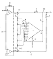
- FIG. 1 An exemplary embodiment of the invention is described in more detail below with reference to the figure explained.
- the figure shows a circuit arrangement for an adjustable High pass.
- the figure contains three amplifier stages 1, 2 and 3, a voltage divider unit 4, a capacitor 5, resistors 6, 7 and 18, a selection unit 8, non-inverting inputs 9, inverting inputs 10 and the output signal 11 of amplifier stage 1.
- the amplifier stages 1, 2 and 3 are each designed as operational amplifiers.
- the Operational amplifier 2 at the input 16 of the circuit arrangement amplifies the Ceramic filter incoming signal with a gain factor k. This reinforced
- the input signal is divided into a main and a secondary flow at point 13.
- the secondary current is switched to a non-inverting input via a voltage divider unit 4, which consists of resistors R 11 to R n .
- the connection points between the individual resistors R 11 to R n are each connected to non-inverting inputs 9 of the operational amplifier 2.
- the inverting inputs 10 are connected to one another and routed to the output 11 of the operational amplifier 1.
- the capacitor 5 is connected to this output 11.
- the secondary current is led to the summing node 12 via the capacitor 5.
- the sum node 12 also represents the output 15 of the high pass.
- Another ohmic resistor 7 is connected from the sum node 12 to a common reference potential 14. This common reference potential 14 is formed by the output of the operational amplifier 3.
- the operational amplifier 1 is controlled in such a way that one of the non-inverting inputs 9 is selected and the partial voltage which arises as a result and which arises at the voltage divider unit 4, the input voltage for the operational amplifier 1.
- Each non-inverting input has a differential amplifier, which is not shown here.
- These differential amplifiers assigned to the respective non-inverting input are activated via a transistor connected as a current source. Due to the different selectable partial voltages, a variable current that is dependent on these partial voltages is produced at the output 11 of the operational amplifier 1 and is supplied to the summing node 12 via the capacitor 5.
- the main current which is led from the output of the operational amplifier 2 via the resistor 6 to the summing node 12 is characterized by a low-pass characteristic.
- the arrangement of the capacitor 5, the operational amplifier 1 and the voltage divider unit 4 ensures that the secondary current is controllable in its amplitude and also in its phase, so that the output signal 15 of the high pass, which is fed to a stereo decoder, as a resultant signal from the Main stream and the side stream is formed and the main stream with the low-pass characteristic and the transmission errors is corrected by the amplitude and phase corrected signal of the side stream.
- the step-wise variable current through the capacitor 5 achieves a result which is equivalent to a variation in the capacitance of the capacitor 5, with the result that an adjustable high-pass filter can be implemented in the overall function.
- an adjustable high-pass filter can be implemented in the overall function.
- the third operational amplifier 3 is an adjustable low noise Reference potential created.
- the operational amplifier 3 is at his non-inverting input connected to an external reference voltage 17.
- This reference voltage 17 is approximately 3.7 V, that is to say between the operating voltage and mass.
- the output of operational amplifier 3 is inverting Input coupled.
- the applied at the output of the operational amplifier 3 Reference potential 14 can be changed by changing the external reference voltage 17 in shift positive and negative directions.
- At this reference potential 14 are the Voltage divider unit 4 and the second resistor 7 connected. To this This creates a reference signal that is free from interference and on which none Signals are transmitted.
- the operational amplifier 2 is on his inverting input supplied with this external reference voltage 17.
- the voltage divider unit 4 can have a linear division. Based on this division creates the corresponding transfer functions of the High-pass filter. With the choice of the size of the capacity to be integrated Capacitor 5 defines the area in which the transfer functions have the high pass changed.
Landscapes
- Engineering & Computer Science (AREA)
- Computer Networks & Wireless Communication (AREA)
- Signal Processing (AREA)
- Networks Using Active Elements (AREA)
- Noise Elimination (AREA)
Claims (7)
- Circuit pour un filtre passe-haut réglable qui contient :caractérisé en ce queune voie principale pour conduire un courant principal avec une première résistance qui est raccordée côté sortie à un noeud de somme,une voie accessoire pour conduire un courant accessoire par l'intermédiaire d'une unité de diviseur de tension, un premier étage amplificateur dont la sortie est couplée aux entrées inversantes du premier étage amplificateur et un condensateur qui est monté entre la sortie du premier étage amplificateur et le noeud de somme,une deuxième résistance qui est raccordée au noeud de somme, le courant principal et le courant accessoire étant additionnés sur le noeud de somme,les entrées non-inversantes du premier étage amplificateur sont respectivement raccordées aux jonctions entre les résistances de l'unité de diviseur de tension et une entrée non-inversante peut être sélectionnée par l'intermédiaire d'une unité de sélection et - l'unité de diviseur de tension et la deuxième résistance sont raccordées à un potentiel de référence réglable et à faible bruit.
- Circuit selon la revendication 1, caractérisé en ce que l'unité de sélection est un bus I2C.
- Circuit selon la revendication 2, caractérisé en ce que les paires de transistors d'entrée des entrées non-inversantes du premier étage amplificateur peuvent être sélectionnées par l'unité de sélection par l'intermédiaire de transistors de sources de courant.
- Circuit selon la revendication 1, caractérisé en ce que l'unité de diviseur de tension présente une répartition non-linéaire.
- Circuit selon la revendication 1, caractérisé en ce qu'un deuxième étage amplificateur qui présente une entrée non-inversante, une entrée inversante et une sortie est prévu pour l'amplification d'un signal d'entrée et la répartition en voies principale et accessoire se produit à la sortie de cet étage amplificateur, un signal de sortie étant contre-couplé de la sortie du deuxième étage d'amplificateur sur son entrée non-inversante, le signal d'entrée du deuxième étage amplificateur est amené à l'entrée non-inversante et l'entrée inversante est commandée avec une tension de référence externe qui se situe entre une tension de fonctionnement et la masse.
- Circuit selon la revendication 5, caractérisé en ce que le potentiel de référence est formé avec un troisième étage amplificateur, le troisième étage amplificateur étant commandé à son entrée non-inversante avec cette tension de référence et une sortie du troisième étage d'amplificateur représentant le potentiel de référence étant contre-couplée sur son entrée inversante.
- Récepteur radio caractérisé par un circuit selon l'une des revendications 1 à 6.
Applications Claiming Priority (2)
| Application Number | Priority Date | Filing Date | Title |
|---|---|---|---|
| DE19802037 | 1998-01-21 | ||
| DE19802037A DE19802037A1 (de) | 1998-01-21 | 1998-01-21 | Schaltungsanordnung für einen verstellbaren Hochpaß |
Publications (3)
| Publication Number | Publication Date |
|---|---|
| EP0932254A2 EP0932254A2 (fr) | 1999-07-28 |
| EP0932254A3 EP0932254A3 (fr) | 2001-02-07 |
| EP0932254B1 true EP0932254B1 (fr) | 2004-05-12 |
Family
ID=7855174
Family Applications (1)
| Application Number | Title | Priority Date | Filing Date |
|---|---|---|---|
| EP99200122A Expired - Lifetime EP0932254B1 (fr) | 1998-01-21 | 1999-01-15 | Circuit filtre passe-haut ajustable |
Country Status (4)
| Country | Link |
|---|---|
| US (1) | US6118332A (fr) |
| EP (1) | EP0932254B1 (fr) |
| JP (1) | JPH11289240A (fr) |
| DE (2) | DE19802037A1 (fr) |
Families Citing this family (6)
| Publication number | Priority date | Publication date | Assignee | Title |
|---|---|---|---|---|
| DE10120108C2 (de) * | 2001-04-25 | 2003-04-30 | Harman Becker Automotive Sys | Verfahren zum Abgleich eines Roll-Off-Kompensationsfilters in einem Stereoempfänger sowie Stereoempfänger |
| US6593804B1 (en) * | 2002-06-25 | 2003-07-15 | National Semiconductor Corporation | Controllable high frequency emphasis circuit for selective signal peaking |
| US7123532B2 (en) | 2003-09-16 | 2006-10-17 | Saifun Semiconductors Ltd. | Operating array cells with matched reference cells |
| US7088082B2 (en) * | 2003-12-16 | 2006-08-08 | Quick Logic Corporation | Regulator with variable capacitor for stability compensation |
| MXPA06008098A (es) * | 2004-01-17 | 2007-03-21 | Optimum Power Technology Lp | Filtro dinamico. |
| US8204466B2 (en) | 2004-05-21 | 2012-06-19 | Realtek Semiconductor Corp. | Dynamic AC-coupled DC offset correction |
Family Cites Families (5)
| Publication number | Priority date | Publication date | Assignee | Title |
|---|---|---|---|---|
| NL8201376A (nl) * | 1982-04-01 | 1983-11-01 | Philips Nv | Schakeling voor het versterken en/of verzwakken van een signaal. |
| JPH05315870A (ja) * | 1992-05-07 | 1993-11-26 | Mitsubishi Electric Corp | 情報処理装置 |
| US5398005A (en) * | 1993-09-28 | 1995-03-14 | National Semiconductor Corporation | Voss tone control circuit with reduced distortion and reduced DC offset |
| DE4431481A1 (de) * | 1994-09-03 | 1996-03-07 | Philips Patentverwaltung | Schaltungsanordnung mit steuerbarem Übertragungsverhalten |
| JP3107006B2 (ja) * | 1996-09-30 | 2000-11-06 | ヤマハ株式会社 | 音場拡大器 |
-
1998
- 1998-01-21 DE DE19802037A patent/DE19802037A1/de not_active Withdrawn
-
1999
- 1999-01-14 US US09/231,065 patent/US6118332A/en not_active Expired - Lifetime
- 1999-01-15 DE DE59909431T patent/DE59909431D1/de not_active Expired - Fee Related
- 1999-01-15 EP EP99200122A patent/EP0932254B1/fr not_active Expired - Lifetime
- 1999-01-18 JP JP11009186A patent/JPH11289240A/ja active Pending
Also Published As
| Publication number | Publication date |
|---|---|
| US6118332A (en) | 2000-09-12 |
| EP0932254A3 (fr) | 2001-02-07 |
| JPH11289240A (ja) | 1999-10-19 |
| DE19802037A1 (de) | 1999-07-22 |
| DE59909431D1 (de) | 2004-06-17 |
| EP0932254A2 (fr) | 1999-07-28 |
Similar Documents
| Publication | Publication Date | Title |
|---|---|---|
| DE69424407T2 (de) | Empfänger mit regelbarem bandpassfilter | |
| DE69306753T2 (de) | Verstärker mit programmierbaren Verstärkungsfaktor | |
| DE3588172T2 (de) | Verstärker mit mehreren Stufen und Frequenzgangkompensation | |
| EP0529119B1 (fr) | Amplificateur intégré monolithique avec commande de gain | |
| DE69431905T2 (de) | Leitungstreiber mit adaptiver ausgangsimpedanz | |
| DE60021170T2 (de) | Verstärker | |
| DE3927873A1 (de) | Entstoerungssystem zur unterdrueckung von stoerung durch nachbarkanal fuer einen fm-empfaenger und verfahren hierfuer | |
| DE69226862T2 (de) | Frequenzabstimmungssystem für ein Paar C-Transkonduktanzoperationsverstärker | |
| DE1904334A1 (de) | Differentialverstaerker fuer vorzugsweise automatische Verstaerkungsregelung | |
| DE2136247A1 (de) | Lautstarkeregelung für Mehrkanal NF Systeme | |
| DE2454631A1 (de) | Entzerrerschaltung | |
| DE4212933A1 (de) | Schaltungsanordnung für einen optischen Empfänger | |
| EP0932254B1 (fr) | Circuit filtre passe-haut ajustable | |
| DE2936507C2 (de) | Graphischer Entzerrer | |
| DE69821197T2 (de) | Differenzverstärker, integrierte schaltung und telefon | |
| DE3131900C2 (de) | FM-Detektor | |
| DE69518624T2 (de) | Verbesserungen einen null-zwischenfrequenz-empfänger betreffend | |
| DE19630416C1 (de) | SC-Filter mit intrinsischer Anti-Aliasing-Funktion sowie damit ausgerüsteter Audiosignalprocessor | |
| DE19630406C1 (de) | Filterschaltung und damit ausgerüsteter Audiosignalprozessor | |
| DE3603841C2 (de) | Dämpfungsglied mit niedrigem Rauschverhalten und hoher thermischer Stabilität | |
| EP0456321B1 (fr) | Circuit comprenant une caractéristique de transfert commandée | |
| DE1512725C3 (de) | Breitbandverstärker mit steuerbarer Verstärkung | |
| DE2928367C2 (de) | Mehrkanal-Signalverarbeitungsschaltung in integrierter Bauweise | |
| DE2739669C2 (de) | Multiplex-Stereo-Dekoder | |
| EP0746122B1 (fr) | Dispositif de mixage pour une console de mixage pour signaux sonores permettant l'intégration monolithique |
Legal Events
| Date | Code | Title | Description |
|---|---|---|---|
| PUAI | Public reference made under article 153(3) epc to a published international application that has entered the european phase |
Free format text: ORIGINAL CODE: 0009012 |
|
| AK | Designated contracting states |
Kind code of ref document: A2 Designated state(s): DE FR GB |
|
| AX | Request for extension of the european patent |
Free format text: AL;LT;LV;MK;RO;SI |
|
| RAP3 | Party data changed (applicant data changed or rights of an application transferred) |
Owner name: KONINKLIJKE PHILIPS ELECTRONICS N.V. Owner name: PHILIPS CORPORATE INTELLECTUAL PROPERTY GMBH |
|
| PUAL | Search report despatched |
Free format text: ORIGINAL CODE: 0009013 |
|
| AK | Designated contracting states |
Kind code of ref document: A3 Designated state(s): AT BE CH CY DE DK ES FI FR GB GR IE IT LI LU MC NL PT SE |
|
| AX | Request for extension of the european patent |
Free format text: AL;LT;LV;MK;RO;SI |
|
| 17P | Request for examination filed |
Effective date: 20010807 |
|
| AKX | Designation fees paid |
Free format text: DE FR GB |
|
| RAP1 | Party data changed (applicant data changed or rights of an application transferred) |
Owner name: KONINKLIJKE PHILIPS ELECTRONICS N.V. Owner name: PHILIPS CORPORATE INTELLECTUAL PROPERTY GMBH |
|
| RAP1 | Party data changed (applicant data changed or rights of an application transferred) |
Owner name: KONINKLIJKE PHILIPS ELECTRONICS N.V. Owner name: PHILIPS INTELLECTUAL PROPERTY & STANDARDS GMBH |
|
| GRAP | Despatch of communication of intention to grant a patent |
Free format text: ORIGINAL CODE: EPIDOSNIGR1 |
|
| GRAS | Grant fee paid |
Free format text: ORIGINAL CODE: EPIDOSNIGR3 |
|
| GRAA | (expected) grant |
Free format text: ORIGINAL CODE: 0009210 |
|
| AK | Designated contracting states |
Kind code of ref document: B1 Designated state(s): DE FR GB |
|
| REG | Reference to a national code |
Ref country code: GB Ref legal event code: FG4D Free format text: NOT ENGLISH |
|
| REF | Corresponds to: |
Ref document number: 59909431 Country of ref document: DE Date of ref document: 20040617 Kind code of ref document: P |
|
| GBT | Gb: translation of ep patent filed (gb section 77(6)(a)/1977) |
Effective date: 20040719 |
|
| REG | Reference to a national code |
Ref country code: GB Ref legal event code: 746 Effective date: 20040721 |
|
| ET | Fr: translation filed | ||
| PGFP | Annual fee paid to national office [announced via postgrant information from national office to epo] |
Ref country code: GB Payment date: 20050127 Year of fee payment: 7 Ref country code: FR Payment date: 20050127 Year of fee payment: 7 |
|
| REG | Reference to a national code |
Ref country code: FR Ref legal event code: D6 |
|
| PGFP | Annual fee paid to national office [announced via postgrant information from national office to epo] |
Ref country code: DE Payment date: 20050315 Year of fee payment: 7 |
|
| PLBE | No opposition filed within time limit |
Free format text: ORIGINAL CODE: 0009261 |
|
| STAA | Information on the status of an ep patent application or granted ep patent |
Free format text: STATUS: NO OPPOSITION FILED WITHIN TIME LIMIT |
|
| 26N | No opposition filed |
Effective date: 20050215 |
|
| PG25 | Lapsed in a contracting state [announced via postgrant information from national office to epo] |
Ref country code: GB Free format text: LAPSE BECAUSE OF NON-PAYMENT OF DUE FEES Effective date: 20060115 |
|
| PG25 | Lapsed in a contracting state [announced via postgrant information from national office to epo] |
Ref country code: FR Free format text: LAPSE BECAUSE OF NON-PAYMENT OF DUE FEES Effective date: 20060131 |
|
| PG25 | Lapsed in a contracting state [announced via postgrant information from national office to epo] |
Ref country code: DE Free format text: LAPSE BECAUSE OF NON-PAYMENT OF DUE FEES Effective date: 20060801 |
|
| GBPC | Gb: european patent ceased through non-payment of renewal fee |
Effective date: 20060115 |
|
| REG | Reference to a national code |
Ref country code: FR Ref legal event code: ST Effective date: 20060929 |