EP0932322A2 - Méthode pour le contrÔle d' un dispositif d' adaptation de la couche ATM et dispositif relatif correspondant - Google Patents
Méthode pour le contrÔle d' un dispositif d' adaptation de la couche ATM et dispositif relatif correspondant Download PDFInfo
- Publication number
- EP0932322A2 EP0932322A2 EP99101401A EP99101401A EP0932322A2 EP 0932322 A2 EP0932322 A2 EP 0932322A2 EP 99101401 A EP99101401 A EP 99101401A EP 99101401 A EP99101401 A EP 99101401A EP 0932322 A2 EP0932322 A2 EP 0932322A2
- Authority
- EP
- European Patent Office
- Prior art keywords
- physical layer
- layer device
- priority
- address
- atm
- Prior art date
- Legal status (The legal status is an assumption and is not a legal conclusion. Google has not performed a legal analysis and makes no representation as to the accuracy of the status listed.)
- Withdrawn
Links
Images


Classifications
-
- H—ELECTRICITY
- H04—ELECTRIC COMMUNICATION TECHNIQUE
- H04Q—SELECTING
- H04Q11/00—Selecting arrangements for multiplex systems
- H04Q11/04—Selecting arrangements for multiplex systems for time-division multiplexing
- H04Q11/0428—Integrated services digital network, i.e. systems for transmission of different types of digitised signals, e.g. speech, data, telecentral, television signals
- H04Q11/0478—Provisions for broadband connections
-
- H—ELECTRICITY
- H04—ELECTRIC COMMUNICATION TECHNIQUE
- H04L—TRANSMISSION OF DIGITAL INFORMATION, e.g. TELEGRAPHIC COMMUNICATION
- H04L12/00—Data switching networks
- H04L12/54—Store-and-forward switching systems
- H04L12/56—Packet switching systems
- H04L12/5601—Transfer mode dependent, e.g. ATM
- H04L2012/5614—User Network Interface
- H04L2012/5616—Terminal equipment, e.g. codecs, synch.
-
- H—ELECTRICITY
- H04—ELECTRIC COMMUNICATION TECHNIQUE
- H04L—TRANSMISSION OF DIGITAL INFORMATION, e.g. TELEGRAPHIC COMMUNICATION
- H04L12/00—Data switching networks
- H04L12/54—Store-and-forward switching systems
- H04L12/56—Packet switching systems
- H04L12/5601—Transfer mode dependent, e.g. ATM
- H04L2012/5638—Services, e.g. multimedia, GOS, QOS
- H04L2012/5646—Cell characteristics, e.g. loss, delay, jitter, sequence integrity
- H04L2012/5651—Priority, marking, classes
-
- H—ELECTRICITY
- H04—ELECTRIC COMMUNICATION TECHNIQUE
- H04L—TRANSMISSION OF DIGITAL INFORMATION, e.g. TELEGRAPHIC COMMUNICATION
- H04L12/00—Data switching networks
- H04L12/54—Store-and-forward switching systems
- H04L12/56—Packet switching systems
- H04L12/5601—Transfer mode dependent, e.g. ATM
- H04L2012/5678—Traffic aspects, e.g. arbitration, load balancing, smoothing, buffer management
- H04L2012/5679—Arbitration or scheduling
Definitions
- the present invention relates to an ATM (Asynchronous Tranfer Mode) layer device for realizing the function of an ATM layer in an ATM transmission network.
- ATM Asynchronous Tranfer Mode
- a protocol for transferring information is constituted of a plurality of layers. Respective layers have inherent functions, and one layer is realized by utilizing the function of a layer inferior to the first named layer by one layer.
- a lower layer which is the most remote layer from a user's side, includes a physical layer and an ATM layer.
- the physical layer is a layer for providing a resource for transferring a cell which is a unit of information transmission, and specifically, executes generation of a signal format suitable to a transmission medium, receiving of a signal, an encoding, or generation and elimination of a transmission frame. Furthermore, the physical layer checks whether or not the information included in the cell is effective, and transfers the cell carrying the effective information (effective cell) to the ATM layer.
- the ATM layer is a layer superior to the physical layer by one layer, and executes a multiplexing and a separation of cells.
- An ATM layer device which is a device realizing the function of the ATM layer and a physical layer device which is a device realizing the function of the physical layer, are connected through for example a UTOPIA interface (one of interface standards).
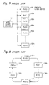
- Fig. 7 is a block diagram illustrating the connection between the ATM layer device and the physical layer devices.
- n physical layer devices 102 1 to 102n (where “n” is positive number) are connected through a UTOPIA interface.
- the ATM layer device 101 selects one from the "n” physical layer devices 102 1 to 102n, and transfers a cell between the ATM layer device and the selected physical layer device.
- the prior art ATM layer device gives an equal opportunity of selection to all the physical layer devices 102 1 to 102n, since the priority order is not provided among the physical layer devices 102 1 to 102n.
- a system for equally selecting the physical layer devices 102 1 to 102n includes for example a round robin scheduling.
- this round robin scheduling as shown in Fig. 8, all the physical layer devices 102 1 to 102n are selected in a predetermined order as if a closed loop is depicted.
- the ATM layer device receives the cell from the plurality of physical layer devices having the low transmission rate, the ATM layer device receives the cell from the physical layer device having the high transmission rate.
- the physical layer device having the high transmission rate transmits the cell to the ATM layer device, it receives a next cell, so that there is possibility that a receiving buffer for temporarily storing the cells causes overflow.
- Another object of the present invention is to provide an ATM layer device capable of preventing the drop of the cell transfer rate and the overflow of the receiving buffer provided in the physical layer device.
- an ATM layer device controlling method realizing the function of an ATM layer by selecting one from a plurality of physical layer devices realizing the function of a physical layer, and executing a transfer of a cell, which is a unit of transmission, between the ATM layer device and the selected physical layer device, the method including the steps of holding the priority information indicating the previously set priority level of each of the plurality of physical layer devices, and selecting the physical layer device which should execute the cell transfer, in a predetermined order in accordance with the priority information.
- the pnority is so set that the larger the transmission rate of the physical layer device is, the higher the priority level of the physical layer device is.
- an ATM layer device configured to realize the function of an ATM layer by selecting one from a plurality of physical layer devices realizing the function of a physical layer, and executing a transfer of a cell, which is a unit of transmission, between the ATM layer device and the selected physical layer device, the ATM layer device including a priority information register holding the priority information indicating the previously set priority level of each of the plurality of physical layer devices, a selecting physical layer address output circuit for outputting the address of the physical layer device which should execute the cell transfer, in a predetermined order in accordance with the priority information, and a control circuit for executing the transfer of the cell between the ATM layer device and the physical layer device designated by the address.
- the ATM layer device further includes a polling physical layer address output circuit for outputting, in the predetermined order, the address of the physical layer device of a candidate which should execute the cell transfer, selected in accordance with the priority information, and wherein the selecting physical layer address output circuit responds to a cell transfer enable notify signal indicating that the cell transfer is possible, outputted from the physical layer device designated from the address, so as to output the address of the physical layer device which should execute the cell transfer.
- the selecting physical layer address output circuit can include a plurality of priority control registers for holding the information of the physical layer devices in units of different levels of the priority
- the polling physical layer address output circuit can include a plurality of priority control registers for holding the information of the physical layer devices in units of different levels of the priority.
- the ATM layer device in accordance with the present invention holds the priority information indicating the previously set priority level of each of a plurality of physical layer devices, and selects the physical layer device which should execute the cell transfer, in the predetermined order in accordance with the priority information. Therefore, the higher the priority level of the physical layer device is, the larger the opportunity of the selection of the physical layer device becomes, so that the data transfer amount per a unit time, of the physical layer device having the high priority level, can be increased.
- the ATM layer device in accordance with the present invention holds priority information indicating a previously set priority level of respective physical layer devices, and selects a physical layer device which should execute a cell transfer, in accordance with the priority information.
- the ATM layer device includes means for realizing the function of the cell multiplexing and the function of the cell separation, but since these means do not have a close relation to the present invention, these means are omitted in the drawing and explanation thereof will be omitted.
- connection between the ATM layer device and the physical layer devices is similar to the prior art (Fig. 7).
- Fig. 1 is a block diagram illustrating the structure of the ATM layer device in accordance with the present invention.
- an ATM layer device 1 is connected to "n" physical layer devices 2 1 to 2n and a host controller 3 for generating a control signal for rewriting the priority information of the physical layer devices 2 1 to 2n.
- the ATM layer device 1 outputs an address of the physical layer device (2 1 to 2n) which should execute the cell transfer, and on the other hand, each of the physical layer devices 2 1 to 2n outputs a cell transfer enable notify signal indicating whether or not the corresponding physical layer device can execute the cell transfer.
- the ATM layer device 1 includes a priority information register 11 for holding the priority information of the respective physical layer devices 2 1 to 2n, a selecting physical layer address output circuit 12 for outputting a first physical layer address which is an address of the physical layer device which should execute the cell transfer (namely, the address of the selected physical layer device), a polling physical layer address output circuit 13 for outputting a second physical layer address which is an address of the physical layer device which is a candidate for selection, a first selector 14 for selecting either of the first physical layer address and the second physical layer address in accordance with a first selection signal outputted from the selecting physical layer address output circuit 12, and a second selector 15 for alternately outputting the physical layer address outputted from the first selector 14 and the data "1" (of the same bit number as that of the physical layer address) in accordance with a second selection signal supplied from a control circuit (not shown), in order to output the address signal defined in the UTOPIA interface.
- a priority information register 11 for holding the priority information of the respective physical layer devices 2 1 to 2n
- the selecting physical layer address output circuit 12 includes a first priority control register 16 1 for holding the information of the physical layer devices having the highest priority, a second priority control register 16 2 for holding the information of the physical layer devices having a middle priority, and a third priority control register 16 3 for holding the information of the physical layer devices having the lowest priority.
- the polling physical layer address output circuit 13 includes a fourth priority control register 17 1 for holding the information of the physical layer devices having the highest priority, a fifth priority control register 17 2 for holding the information of the physical layer devices having a middle priority, and a sixth priority control register 17 3 for holding the information of the physical layer devices having the lowest priority.
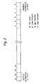
- Fig. 2 is a diagram illustrating one example of the content stored in the priority information register 11 shown in Fig. 1
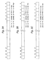
- Figs. 3A, 3B and 3C are diagrams illustrating the contents of the priority control registers shown in Fig. 1
- Fig. 3A is a diagram illustrating the contents of the first and fourth priority control registers 16 1 and 17 1
- Fig. 3B is a diagram illustrating the contents of the second and fifth priority control registers 16 2 and 17 2
- Fig. 3C is a diagram illustrating the contents of the third and sixth priority control registers 16 3 and 17 3 .
- the priority information of each of the physical layer devices 2 1 to 2n is stored in the priority information register 11 in units of two bits.
- the data "1" is written into the bit(s) corresponding to the physical layer device(s) having the highest priority.
- Fig. 2 and Figs. 3A, 3B and 3C illustrate the examples of the contents stored in the priority information register 11, the first to third priority control registers 16 1 to 1 63 and the fourth to sixth priority control registers 17 1 to 17 3 in the case having 31 physical layer devices.
- the priority control registers are provided in accordance with the number of priority levels. For example, when the priority has two levels (namely, a high priority and a low priority), it is sufficient if each of the selecting physical layer address output circuit 12 and the polling physical layer address output circuit 13 includes two priority control registers.
- the priority information register 11 is previously written with the priority information as shown in Fig. 2, of the respective physical layer devices 2 1 to 2n, by the host controller 3.
- the ATM layer device 1 firstly outputs from the polling physical layer address output circuit 13 the second physical layer address which is the address of the physical layer device of the selection candidate.
- the selecting physical layer address output circuit 12 outputs the first selection signal causing the first selector 14 to output the second physical layer address.
- the second selector 15 alternately outputs the second physical layer address outputted from the first selector 14 and the data "1" of the bit number equal to that of the second physical layer address, in accordance with the second selection signal, so as to transmit it to the selecting physical layer address output circuit 12 and the physical layer devices 2 1 to 2n.
- the physical layer device designated by the second physical layer address outputs the cell transfer enable notify signal indicating whether or not the cell transfer is possible, to the selecting physical layer address output circuit 12.
- the selecting physical layer address output circuit 12 receives the second physical layer address outputted from the second selector 15 and the cell transfer enable notify signal outputted from the physical layer device designated by the second physical layer address, and outputs the address of the physical layer device which can execute the cell transfer (first physical layer address) and simultaneously outputs the first selection signal causing the first selector 14 to output the first physical layer address.
- the second selector 15 alternately outputs the first physical layer address outputted from the first selector 14 and the data "1" of the bit number equal to that of the first physical layer address, in accordance with the second selection signal, so as to transmit it to the selecting physical layer address output circuit 12 and the physical layer devices 2 1 to 2n.
- the physical layer device designated by the first physical layer address executes the cell tranfer between the physical layer device designated by the second physical layer address and a control circuit (not shown) provided in the ATM layer device.
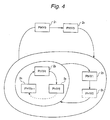
- the 31 physical layer devices are divided into the physical layer devices PHY0 and PHY3 having the highest priority, the physical layer devices PHY1 and PHY2 having the middle priority and the physical layer devices PHY4 to PHY30 having the lowest priority.
- the physical layer devices are selected by in the order determined by a priority-based hierarchical combination of a loop constituted of the physical layer devices having the highest priority, another loop constituted of the physical layer devices having the middle priority, and still another loop constituted of the physical layer devices having the lowest priority, as in the named order of PHY0, PHY3, PHY1, PHY0, PHY3, PHY2, PHY0, PHY3, PHY4, PHY0, • • •.
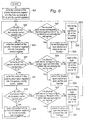
- Fig. 5 is a flowchart illustrating the procedures of the processing in the polling physical layer address output circuit shown in Fig. 1
- Fig. 6 is a flowchart illustrating the procedures of the processing in the selecting physical layer address output circuit shown in Fig. 1.
- the polling physical layer address output circuit 13 firstly writes the priority information of the respective physical layer devices 2 1 to 2n to the fourth to sixth priority control registers 17 1 to 17 3 on the basis of the content of the priority information register 11 (step S1).
- the polling physical layer address output circuit 13 ascertains whether or not all the bits of the fourth priority control register 17 1 are "0" (step S2). If all the bits of the fourth priority control register 17 1 are not "0", the polling physical layer address output circuit 13 outputs the address of the physical layer device corresponding to the least significant bit of the "1"-written bits in the fourth priority control register 17 1 (the second physical layer address) (step S3).
- the polling physical layer address output circuit 13 rewrites the bit of the fourth priority control register 17 1 corresponding to the physical layer device selected in the step S3, to "0" (step S4), and returns to the step 2 so as to repeat the processing of the steps S2 to S4 until all the bits of the fourth priority control register 17 1 become "0".
- the polling physical layer address output circuit 13 writes again the priority information of the corresponding physical layer devices (2 1 and 2 4 in the example of Fig. 4) to the fourth priority control register 17 1 on the basis of the content of the priority information register 11 (step S5).
- step S6 the polling physical layer address output circuit 13 ascertains whether or not all the bits of the fifth priority control register 17 2 are "0". If all the bits of the fifth priority control register 17 2 are not "0", the polling physical layer address output circuit 13 outputs the address of the physical layer device corresponding to the least significant bit of the "1"-written bits in the fifth priority control register 17 2 (the second physical layer address) (step S7).
- the polling physical layer address output circuit 13 rewrites the bit of the fifth priority control register 17 2 corresponding to the physical layer device selected in the step S7, to "0" (step S8), and returns to the step 2.
- the polling physical layer address output circuit 13 writes again the priority information of the corresponding physical layer devices (2 2 and 2 3 in the example of Fig. 4) to the fifth priority control register 17 2 on the basis of the content of the priority information register 11 (step S9).
- step S10 the polling physical layer address output circuit 13 ascertains whether or not all the bits of the sixth priority control register 17 3 are "0". If all the bits of the sixth priority control register 17 3 are not "0", the polling physical layer address output circuit 13 outputs the address of the physical layer device corresponding to the least significant bit of the "1"-written bits in the sixth priority control register 17 3 (the second physical layer address) (step S11).
- the polling physical layer address output circuit 13 rewrites the bit of the sixth priority control register 17 3 corresponding to the physical layer device selected in the step S11, to "0" (step S12), and returns to the step 2.
- the polling physical layer address output circuit 13 writes again the priority information of the corresponding physical layer devices (2 5 to 2n in the example of Fig. 4) to the sixth priority control register 17 3 on the basis of the content of the priority information register 11 (step S13). Therefore, the processing returns to the step S2, so that the processing of the steps S2 to S13 is repeated.
- the polling physical layer address output circuit 13 outputs the physical layer address in the order determined by the priority-based hierarchical combination of a high priority loop composed of the physical layer devices having the highest priority, a middle priority loop composed of the physical layer devices having the middle priority, and a low priority loop composed of the physical layer devices having the lowest priority, as shown in Fig. 4.
- the selecting physical layer address output circuit 12 firstly writes the priority information of the respective physical layer devices 2 1 to 2n into the first, second and third priority control registers 16 1 to 16 3 on the basis of the content of the priority information register 11 (step S21).
- the selecting physical layer address output circuit 12 ascertains whether or not all the contents of the first priority control register 16 1 are "0" (step S22). when all the contents of the first priority control register 16 1 are not "0", the selecting physical layer address output circuit 12 ascertains whether or not the physical layer device corresponding to the least significant bit of the "1"-written bits can execute the cell transfer (step S23). Whether or not the cell transfer is executable, is discriminated on the basis of the second physical layer address and the cell transfer enable notify signal outputted from the physical layer device designated by the second physical layer address.
- the selecting physical layer address output circuit 12 When the result of the processing in the step S23 indicates that the cell transfer is possible, the selecting physical layer address output circuit 12 outputs the address of the corresponding physical layer device (first physical layer address), so that the cell transfer is executed between the ATM layer device and the corresponding physical layer device (step S24). On the other hand, when the cell transfer is not possible, or when the processing in the step S24 is completed, the selecting physical layer address output circuit 12 rewrites the least significant bit of the "1"-written bits in the first priority control register 16 1 to "0" (step S25), and the processing returns to the step S22 so that the processing of the steps S22 to S25 is repeated until all the contents of the first priority control register 16 1 become "0".
- the selecting physical layer address output circuit 12 writes again the priority information of the corresponding physical layer devices (2 1 and 2 4 in the example of Fig. 4) to the first priority control register 16 1 on the basis of the content of the priority information register 11 (step S26).
- step S26 the processing goes into a step S27 in which the selecting physical layer address output circuit 12 ascertains whether or not all the bits of the second priority control register 16 2 are "0". If all the bits of the second priority control register 16 2 are not "0", the selecting physical layer address output circuit 12 ascertains whether or not the physical layer device corresponding to the least significant bit of the "1"-written bits can execute the cell transfer (step S28).
- step S28 the selecting physical layer address output circuit 12 outputs the address of the corresponding physical layer device (first physical layer address), so that the cell transfer is executed between the ATM layer device and the corresponding physical layer device (step S29).
- the selecting physical layer address output circuit 12 rewrites the least significant bit of the "1"-written bits in the second priority control register 16 2 to "0" (step S30), and the processing returns to the step S22.
- the selecting physical layer address output circuit 12 writes again the priority information of the corresponding physical layer devices (2 2 and 2 3 in the example of Fig. 4) to the second priority control register 16 2 on the basis of the content of the priority information register 11 (step S31).
- step S31 the processing goes into a step S32 in which the selecting physical layer address output circuit 12 ascertains whether or not all the bits of the third priority control register 16 3 are "0". If all the bits of the third priority control register 16 3 are not "0", the selecting physical layer address output circuit 12 ascertains whether or not the physical layer device corresponding to the least significant bit of the "1"-written bits can execute the cell transfer (step S33).
- step S33 the selecting physical layer address output circuit 12 outputs the address of the corresponding physical layer device (first physical layer address), so that the cell transfer is executed between the ATM layer device and the corresponding physical layer device (step S34).
- the selecting physical layer address output circuit 12 rewrites the least significant bit of the "1"-written bits in the third priority control register 16 3 to "0" (step S35), and the processing returns to the step S22.
- the selecting physical layer address output circuit 12 writes again the priority information of the corresponding physical layer devices (2 5 to 2n in the example of Fig. 4) to the third priority control register 16 3 on the basis of the content of the priority information register 11 (step S36), and the processing returns to the step S22, so that the processing of the steps S22 to S36 is repeated.
- the selecting physical layer address output circuit 12 outputs the physical layer address in the order determined by the priority-based hierarchical combination of a high priority loop composed of the physical layer devices having the highest priority, a middle priority loop composed of the physical layer devices having the middle priority, and a low priority loop composed of the physical layer devices having the lowest priority, as shown in Fig. 4.
- the ATM layer device in accordance with the present invention holds the priority information indicating the previously set priority level of each of a plurality of physical layer devices, and selects the physical layer device which should execute the cell transfer, in the predetermined order in accordance with the priority information. Therefore, the higher the priority level of the physical layer device is, the larger the opportunity of the selection of the physical layer device becomes, so that the data transfer amount per a unit time, of the physical layer device having the high priority level, can be increased.
Landscapes
- Engineering & Computer Science (AREA)
- Computer Networks & Wireless Communication (AREA)
- Data Exchanges In Wide-Area Networks (AREA)
- Communication Control (AREA)
Applications Claiming Priority (3)
| Application Number | Priority Date | Filing Date | Title |
|---|---|---|---|
| JP1285298A JP3169070B2 (ja) | 1998-01-26 | 1998-01-26 | Atmレイヤデバイスの制御方法及びatmレイヤデバイス |
| JP1285298 | 1998-01-26 | ||
| US09/238,091 US6510155B1 (en) | 1998-01-26 | 1999-01-26 | ATM layer device controlling method and ATM layer device |
Publications (2)
| Publication Number | Publication Date |
|---|---|
| EP0932322A2 true EP0932322A2 (fr) | 1999-07-28 |
| EP0932322A3 EP0932322A3 (fr) | 2002-11-06 |
Family
ID=26348536
Family Applications (1)
| Application Number | Title | Priority Date | Filing Date |
|---|---|---|---|
| EP99101401A Withdrawn EP0932322A3 (fr) | 1998-01-26 | 1999-01-26 | Méthode pour le contrôle d' un dispositif d' adaptation de la couche ATM et dispositif relatif correspondant |
Country Status (3)
| Country | Link |
|---|---|
| US (1) | US6510155B1 (fr) |
| EP (1) | EP0932322A3 (fr) |
| JP (1) | JP3169070B2 (fr) |
Cited By (1)
| Publication number | Priority date | Publication date | Assignee | Title |
|---|---|---|---|---|
| WO2002073905A1 (fr) * | 2001-03-13 | 2002-09-19 | Adc Telecommunications Israel Ltd. | Organisation de la priorite pour divers dispositifs a couche physique au niveau d'une interface utopique |
Families Citing this family (7)
| Publication number | Priority date | Publication date | Assignee | Title |
|---|---|---|---|---|
| JP2001230781A (ja) * | 2000-02-16 | 2001-08-24 | Fujitsu Ltd | 通信制御装置 |
| CA2313087A1 (fr) * | 2000-06-29 | 2001-12-29 | Pmc-Sierra, Inc. | Interface de bus pour transferts de donnees par cellules et/ou par paquets |
| JP2002044084A (ja) * | 2000-07-19 | 2002-02-08 | Fujitsu Ltd | 非同期転送モードレイヤ側インターフェース装置,物理レイヤ側インターフェース装置及びセル処理方法 |
| US7990989B2 (en) * | 2006-09-16 | 2011-08-02 | Mips Technologies, Inc. | Transaction selector employing transaction queue group priorities in multi-port switch |
| US7773621B2 (en) * | 2006-09-16 | 2010-08-10 | Mips Technologies, Inc. | Transaction selector employing round-robin apparatus supporting dynamic priorities in multi-port switch |
| US7961745B2 (en) * | 2006-09-16 | 2011-06-14 | Mips Technologies, Inc. | Bifurcated transaction selector supporting dynamic priorities in multi-port switch |
| US7760748B2 (en) * | 2006-09-16 | 2010-07-20 | Mips Technologies, Inc. | Transaction selector employing barrel-incrementer-based round-robin apparatus supporting dynamic priorities in multi-port switch |
Family Cites Families (3)
| Publication number | Priority date | Publication date | Assignee | Title |
|---|---|---|---|---|
| KR960003505B1 (ko) * | 1992-12-29 | 1996-03-14 | 재단법인 한국전자통신연구소 | 에이티엠(atm) 다중화 처리 장치 |
| US5485456A (en) * | 1994-10-21 | 1996-01-16 | Motorola, Inc. | Asynchronous transfer mode (ATM) system having an ATM device coupled to multiple physical layer devices |
| CA2181293C (fr) * | 1995-07-17 | 2000-06-06 | Charles Kevin Huscroft | Dispositif a couche mta |
-
1998
- 1998-01-26 JP JP1285298A patent/JP3169070B2/ja not_active Expired - Fee Related
-
1999
- 1999-01-26 EP EP99101401A patent/EP0932322A3/fr not_active Withdrawn
- 1999-01-26 US US09/238,091 patent/US6510155B1/en not_active Expired - Fee Related
Non-Patent Citations (4)
| Title |
|---|
| ATM FORUM: "UTOPIA LEVEL 2, VERSION 1.0" ATM FORUM TECHNICAL COMMITTEE, XX, XX, 1 June 1995 (1995-06-01), pages 1-66, XP002098753 * |
| CHANGHWAN OH ET AL: "PRIORITY CONTROL ATM FOR SWITCHING SYSTEMS" IEICE TRANSACTIONS ON COMMUNICATIONS, INSTITUTE OF ELECTRONICS INFORMATION AND COMM. ENG. TOKYO, JP, vol. E75 - B, no. 9, 1 September 1992 (1992-09-01), pages 894-904, XP000321325 ISSN: 0916-8516 * |
| CHIUSSI F M ET AL: "THE ATLANTA ARCHITECTURE AND CHIPSET: A LOW-COST SCALABLE SOLUTION FOR ATM NETWORKING" ISS '97. WORLD TELECOMMUNICATIONS CONGRESS. (INTERNATIONAL SWITCHING SYMPOSIUM). GLOBAL NETWORK EVOLUTION: CONVERGENCE OR COLLISION? TORONTO, SEPT. 21 - 26, 1997, ISS. WORLD TELECOMMUNICATIONS CONGRESS. (INTERNATIONAL SWITCHING SYMPOSIUM), TORONTO, P, vol. 1, 21 September 1997 (1997-09-21), pages 43-52, XP000720505 * |
| GALLASSI G ET AL: "RESOURCE MANAGEMENT AND DIMENSIONING IN ATM NETWORKS" IEEE NETWORK, IEEE INC. NEW YORK, US, vol. 4, no. 3, May 1990 (1990-05), pages 8,11-17, XP000160043 ISSN: 0890-8044 * |
Cited By (1)
| Publication number | Priority date | Publication date | Assignee | Title |
|---|---|---|---|---|
| WO2002073905A1 (fr) * | 2001-03-13 | 2002-09-19 | Adc Telecommunications Israel Ltd. | Organisation de la priorite pour divers dispositifs a couche physique au niveau d'une interface utopique |
Also Published As
| Publication number | Publication date |
|---|---|
| JPH11215141A (ja) | 1999-08-06 |
| JP3169070B2 (ja) | 2001-05-21 |
| EP0932322A3 (fr) | 2002-11-06 |
| US6510155B1 (en) | 2003-01-21 |
Similar Documents
| Publication | Publication Date | Title |
|---|---|---|
| EP0378195B1 (fr) | Dispositif de tampon apte à la communication au mode de transfert asynchrone | |
| CA2329542C (fr) | Systeme et procede d'ordonnancement de transmission et de traitement de messages dans un reseau de donnees numeriques | |
| US6414961B1 (en) | ATM switching with virtual circuit FIFO buffers | |
| US6262989B1 (en) | Apparatus and method for providing different quality of service connections in a tunnel mode | |
| EP0949839B1 (fr) | Système de transmission de cellules ATM | |
| JPH10215264A (ja) | 動的スケジュールテーブルを利用するスケジューラ | |
| AU3867999A (en) | System and method for regulating message flow in a digital data network | |
| WO1991002420A1 (fr) | Element et procede de commutation de communications servant a la transmission de cellules de longueur variable | |
| EP0932322A2 (fr) | Méthode pour le contrÔle d' un dispositif d' adaptation de la couche ATM et dispositif relatif correspondant | |
| US20020146033A1 (en) | Self-route multi-memory packet switch adapted to have an expandable number of input/output ports | |
| JP2628701B2 (ja) | 優先順位付き情報パケット用交換装置 | |
| US5343467A (en) | Space/time switching element having input/output circuits each separately switchable between two or more bit rates | |
| US6912566B1 (en) | Memory device and method for operating the memory device | |
| KR100400172B1 (ko) | Atm층디바이스의 제어방법 및 atm층디바이스 | |
| JPH10150443A (ja) | Atm交換装置 | |
| US6335940B1 (en) | Digital data exchange device | |
| EP1142220B1 (fr) | Mecanisme de commande d'etat approximatif | |
| US7130302B2 (en) | Self-route expandable multi-memory packet switch | |
| CA2310813C (fr) | Dispositif et methode de surveillance d'etat de file d'attente dans un commutateur a mode de transfert asynchrone | |
| JP3099325B2 (ja) | クロスバスイッチ装置及びその制御方法 | |
| JP3155164B2 (ja) | マルチクラスデータ通信方法,データ交換機およびデータ端末 | |
| JP2965385B2 (ja) | マルチバスにおけるデータセルの転送方式 | |
| JPH04104540A (ja) | 多重化装置 | |
| JP2923891B2 (ja) | 連続セル受信情報転送方法および連続セル受信情報転送システム | |
| US20040078479A1 (en) | Traffic generator using a network processor |
Legal Events
| Date | Code | Title | Description |
|---|---|---|---|
| PUAI | Public reference made under article 153(3) epc to a published international application that has entered the european phase |
Free format text: ORIGINAL CODE: 0009012 |
|
| AK | Designated contracting states |
Kind code of ref document: A2 Designated state(s): AT BE CH CY DE DK ES FI FR GB GR IE IT LI LU MC NL PT SE |
|
| AX | Request for extension of the european patent |
Free format text: AL;LT;LV;MK;RO;SI |
|
| PUAL | Search report despatched |
Free format text: ORIGINAL CODE: 0009013 |
|
| AK | Designated contracting states |
Kind code of ref document: A3 Designated state(s): AT BE CH CY DE DK ES FI FR GB GR IE IT LI LU MC NL PT SE |
|
| AX | Request for extension of the european patent |
Free format text: AL;LT;LV;MK;RO;SI |
|
| RIC1 | Information provided on ipc code assigned before grant |
Free format text: 7H 04Q 11/04 A, 7H 04L 12/56 B |
|
| 17P | Request for examination filed |
Effective date: 20030220 |
|
| RAP1 | Party data changed (applicant data changed or rights of an application transferred) |
Owner name: NEC ELECTRONICS CORPORATION |
|
| 17Q | First examination report despatched |
Effective date: 20030403 |
|
| AKX | Designation fees paid |
Designated state(s): DE FR GB IT |
|
| STAA | Information on the status of an ep patent application or granted ep patent |
Free format text: STATUS: THE APPLICATION IS DEEMED TO BE WITHDRAWN |
|
| 18D | Application deemed to be withdrawn |
Effective date: 20040608 |